Note: Descriptions are shown in the official language in which they were submitted.
CA 02317350 2000-09-05
TITLE OF INVENTION
POWER CONVERTER APPARATUS
BACKGROUND OF THE INVENTION
FIELD OF THE INVENTION
This invention relates to a power converter apparatus
that uses high-speed semiconductor switching devices and
includes a snubber circuit for restraining a surge voltage, and
especially to a wiring structure of the snubber circuit.
DESCRIPTION OF THE BACKGROUND
In recent years, power semiconductor switching
devices for power converters or power inverters remarkably
advance in high-speed switching. For example, GCT (Gate-
communicated Thyristor) is a current gate trigger type of high-
speed semiconductor switching device, and IGBT (Insulated Gate
Bipolar Transistor) and IEGT (Injection Enhanced Gate
Transistor) are voltage gate trigger types of high-speed
semiconductor switching devices. These high-speed
semiconductor switching devices, which are capable of switching
a voltage of 3-6 KV (Kilo-Volts) and a current of
1
CA 02317350 2000-09-05
3-4 KA (Kilo-Amperes), have been developed and made practical.
Further, since a dV/dt resistance of a semiconductor switching
device at a time of turning of f has been improved, it is attempted
that a snubber circuit is made smaller in size and less loss.
FIG. 1 is a circuit diagram showing a conventional NPC
(Neutral Point Clamped) inverter that uses GTO (Gate Turn-off
Thyristor) as a semiconductor switching device. Snubber
circuits 2a, 3a, 4a and 5a are respectively connected to GTO
switching devices 2, 3, 4 and 5. Each of the snubber circuits
2a-5a restrains a surge voltage generated at switching the
GTO switching devices 2-5 and includes a capacitor, a diode
and a resistor.
In recent years, as highly efficient GCT, IGBT and IEGT
are put to practical use, a cramp snubber circuit or a capacitor
are come to be connected to a DC (Direct Current) power source.
These high-speed semiconductor switching devices are able to
switch off a current of several KA (Kilo-Amperes) up to 0 (zero)
in 1-2 micro-seconds as a matter of their behavior. At the
time of switching off a large current, a surge voltage
represented by the product of a wiring inductance and a rise
rate of current (dI/dt) is generated. If a peak of the surge
voltage or a rise rate of voltage (dV/dt) are beyond capacity
to resist voltage of a semiconductor switching device, the
semiconductor switching device may be broken for ever.
Therefore, it is important that the surge voltage be less than
the capacity to resist voltage of the semiconductor switching
2
CA 02317350 2000-09-05
device.
However, in a large capacity type of power converter that
uses high-speed semiconductor switching devices, since either
one of a charge and discharge snubber circuit or a clamp snubber
circuit is connected to each of the semiconductor switching
devices, the power converter becomes large in size and costly.
Accordingly, it is desired to provide a device to restrain
a surge voltage by only cramp snubber circuit connected to
a DC power source in the same way as a power converter using
semiconductor switching devices having small capacity to
resist voltage. That is, it is desired to provide a device
to restrain a surge voltage without attaching a snubber circuit
to each of the semiconductor switching devices.
SUMMARY OF THE INVENTION
Accordingly, one object of this invention is to provide
a power converter apparatus which may reduce a surge voltage
generated at switching a semiconductor switching device and
protect the semiconductor switching device from the surge
voltage.
The presentinvention provides a power converter apparatus,
including a DC power source, a semiconductor stack, connected
to the DC power source in parallel, having a plurality of
semiconductor devices and a cooler for refrigerating the
semiconductor devices, the semiconductor devices and the
cooler are stacked and pressured to each other, and a snubber
3
CA 02317350 2000-09-05
circuit, connected to the DC power source in parallel, having
a serial circuit of a capacitor and a diode, and a resistor
connected inparallel to the diode, one terminal of the capacitor
is disposed adj acent to the semiconductor stack so that magnetic
flux generated by current flowing in the terminal cancels
magnetic flux caused by current flowing in the semiconductor
stack.
BRIEF DESCRIPTION OF THE DRAWINGS
A more complete appreciation of the invention and many
of the attendant advantages thereof will be readily obtained
as the same becomes better understood by reference to the
following detailed description when considered in connection
with the accompanying drawings, wherein:
FIG. 1 is a circuit diagram showing a main circuit of a
conventionalthree- levelNPCinverter apparatus that uses GTO;
FIG. 2 is a circuit diagram showing a main circuit of a
three-level NPC inverter apparatus of a first embodiment of
the present invention;
FIG. 3 is a schematic front view of a semiconductor stack
of the first embodiment;
FIG. 4 is a perspective view of the semiconductor stack
of the first embodiment;
FIG. 5 is a perspective view of a neutral point bus-bar
of the first embodiment;
FIG. 6 is a circuit diagram showing current flows of a
4
CA 02317350 2000-09-05
U-phase circuit of the NPC inverter apparatus of the first
embodiment;
FIG. 7 shows a wave form of a surge voltage that applies
to a semiconductor switching device of the NPC inverter
apparatus of the first embodiment;
FIG. 8 shows a wave form of a transient ON voltage of a
diode of the NPC inverter apparatus of the first embodiment;
and
FIG. 9 is a schematic front view of a semiconductor stack
of an NPC inverter apparatus of a second embodiment.
DETAILED DESCRIPTION OF THE PREFERRED EMBODIMENT
The present invention is hereinafter described in detail
by way of an illustrative embodiment.
(First embodiment)
A three-level NPC inverter apparatus using IEGT of a first
embodiment of the present invention is explained referring
to FIGs. 2-8.
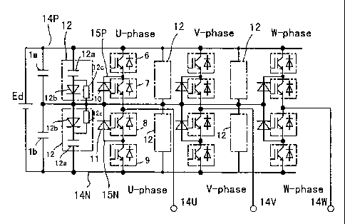
As shown in FIG. 2, a main circuit of the NPC inverter
apparatus of the first embodiment includes a DC power source
having smoothing capacitors la and lb, a U-phase circuit, a
V-phase circuit and a W-phase circuit. The capacitor la is
connected between a positive electrode of the DC power source
and a neutral point thereof. The capacitor lb is connected
between a negative electrode of the DC power source and the
neutral point thereof. The respective U, V and W-phase
CA 02317350 2000-09-05
circuits are connected to the DC power source and have the
same formation each other. The U-phase circuit includes
semiconductor switching devices 6, 7, 8 and 9, first and second
connecting diodes 10 and 11, and two snubber circuits 12. Each
of the semiconductor switching devices 6-9 includes an IEGT
and a diode connected in anti-parallel to the IEGT. The
respective snubber circuits 12 are connected between the
positive electrode and the neutral point, and the negative
electrode and the neutral point respectively. Each of the
snubber circuits 12 includes a snubber capacitorl2a, a snubber
diode 12b and a discharge resistor 12c.
A semiconductor stack 18 mounting the above described main
circuit is hereinafter described.
In general, the main circuit is refrigerated by an
air-cooling or a water-cooling.
FIGs. 3 and 4 show a water-cooling type of the semiconductor
stack 18 that includes the U-phase circuit in FIG. 2. Cooling
pipes 31 for the water cooling are shown in FIG. 4.
As shown in FIGs. 3 and 4, the first and second connecting
diodes 10 and 11, which are connected in serial to each other
putting a neutral point bus-bar 14C, are disposed in the middle
of the semiconductor stack 18. That is, the bus-bar 14C is
connected to a neutral point of the first and second connecting
diodes 10 and 11. In FIG. 3, the right side of the neutral
point is a positive side of the DC power source, and the left
side of the neutral point is a negative side of the DC power
6
CA 02317350 2000-09-05
source. The first connecting diode 10, an insulating spacer
16, the semiconductor switching devices 6 and 7, and cooling
fins 13 for refrigerating the semiconductor switching devices
6 and 7 are disposed on the positive side of the semiconductor
stack 18. Likewise, the second connecting diode 11, an
insulating spacer 16, the semiconductor switching devices 8
and 9, and cooling fins 13 for refrigerating the semiconductor
switching devices 8 and 9 are disposed on the negative side
of the semiconductor stack 18.
The semiconductor switching devices 6-9, the connecting
diodes 10 and 11, the cool ing f ins 13, and the insulat ing spacers
16 are stacked and pressured to each other at a predetermined
pressure.
The semiconductor stack 18 as constructed above is
connected to the DC power source and the snubber circuits 12.
Each case 12a1 of the snubber capacitors 12a is made of
brass or the like and forms terminal. The cases 12a1 are
disposed adj acent to the semiconductor stack 18 so that magnetic
flux generated by current flowing in the case 12a1 (terminal)
cancels magnetic flux caused by current flowing in the
semiconductor stack 18, and connected to the cooling fins 13
directly. Each of the other terminals of the snubber
capacitors 12a is divided into six terminals and includes an
insulator 12a2 insulating from the case 12a1 as shown in FIG.
4. The respective plural termainals are connectedtoterminals
(an anode or a cathode) of the snubber diodes 12b. The other
7
CA 02317350 2000-09-05
terminals of the snubber diodes 12b are the neutral point and
are directly connected to a cooling fin 17 for refrigerating
the snubberdiodes 12b. That is, the cooling fin 17 is connected
to the neutral point.
As shown in FIG. 5, the cooling fin 17 that functions to
connect the terminals of the snubber diodes 12b and to
refrigerate the snubber diodes 12b is secured to the neutral
point bus-bar 14C forming a neutral point of the NPC inverter
apparatus. As shown in FIGs. 3 and 5, the bus-bar 14C is fixed
between an anode and a cathode of the connecting diodes 10
and 11 disposed in a middle of the semiconductor stack 18 and
formed in a shape of T. An area of a fixing plane 32 of the
T-shaped bus-bar 14C is larger than an area of a fixing plane
33 of the cooling fin 17.
In the above description, although the bus-bar 14C is formed
in a shape of T, the bus-bar may be shaped in an inverse L.
In this case, an anode and a cathode of the connecting diodes
and 11 are connected to the L-shaped bus-bar. As long as
an area of a fixing plane of the L-shaped bus-bar is more than
half area of the fixing plane 33 of the cooling fin 17, the
same effect as the T-shaped bus-bar 14C may be achieved.
In the semiconductor stack 18 of the first embodiment,
electric modes of the NPC inverter apparatus that outputs a
positive level, a neutral level and a negative level are
explained referring to FIGs. 3 and 6.
A description of an output mode of the negative level is
8
CA 02317350 2000-09-05
omitted, because a current direction of an output mode of the
positive level is merely reversed.
An arrow A in FIG. 6 shows an output mode of the positive
level of the U-phase circuit.
A current flows in a course of a positive bus-bar 14P,
the semiconductor switching device 6, the semiconductor
switching device 7, and an output bus-bar 14U. As to the
semiconductor stack 18 having the semiconductor switching
devices 6 and 7 shown in FIG. 3, a current flows in a course
of the positive bus-bar 14P, the cooling fin 13, the
semiconductor switching device 6, the cooling fin 13, the
semiconductor switching device 7, the cooling fin 13, and the
output bus-bar 14U as indicated by an arrow A in FIG. 3.
Arrows B and C in FIG. 6 show an output mode of the neutral
level of the U-phase circuit.
A current flows in a course of the neutral point bus-bar
14C, the connecting diode 10, the semiconductor switching
device 7, the output bus-bar 14U, the semiconductor switching
device 8, the connecting diode 11, and the neutral point bus-bar
14C. As to the semiconductor stack 18 having the connecting
diode 10 and the semiconductor switching device 7 shown in
FIG. 3, a current flows in a course of the bus-bar 14C, the
connecting diode 10, the cooling fin 13, a bus-bar 15P, the
cooling fin 13, the semiconductor switching device 7, the
cooling fin 13, and the output bus-bar 14U as indicated by
the arrow B in FIG. 3, and further a current flows in a course
9
CA 02317350 2000-09-05
of the output bus-bar 14U, the cooling fin 13, the semiconductor
switching device 8, the cooling fin 13, a bus-bar 15N, the
cooling fin 13, the connecting diode 11 and the neutral point
bus-bar 14C.
The reason that a surge voltage is generated at the output
modes is explained referring to FIG. 7.
Where a current IL flows in a condition that the
semiconductor switching devices 6 and 7 turn on, if a gate
voltage Vge of the semiconductor switching device 6 is made
negative bias at a time tl shown in FIG. 7, the semiconductor
switching device 6 turns off, thereby increasing a voltage
applying to the semiconductor switching device 6 and reducing
a current Ic flowing into the semiconductor switching device
6. A surge voltage, which is caused by a rate of the current
change (-dI/dt) and a wiring inductance of the main circuit
of the NPC inverter apparatus, is applied to the semiconductor
switching device 6. A surge voltage Vsl generated at a time
t2 in FIG. 7 is represented by the following formula 1. To
restrain the surge voltage, it is needed to reduce the wiring
inductance and to provide a diode that possesses a low transient
ON voltage.
(Formula 1)
Ysl = Va + L * ~ + Vfr
A surge voltage Vs2 generated at a time t3 in FIG. 7 is
represented by the following formula 2.
CA 02317350 2000-09-05
(Formula 2)
Vs2 = Vo + F * Ic
Vo is a DC voltage. Lo is a wiring inductance from the
smoothing capacitor la to the snubber circuit 12. L is the
sum of wiring inductances of L1, L2, L3, L4 and L5. C is a
capacityof the snubber capacity. Vfr is a transient ONvoltage
of the snubber diode 12b.
According to the first embodiment, since each of the cases
12a1 of the snubber capacitors 12a itself forms a terminal
connected to the cooling fin 13 directly and the terminals
of the snubber capacitors 12a are disposed adjacent to the
semiconductor stack 18 so that magnetic flux generated by
current flowing in the terminals cancels magnetic flux caused
by current flowing in the semiconductor stack 18, a wiring
inductance of the NPC inverter apparatus may be minimized,
thereby restraining a surge voltage that applies to the
semiconductor switching devices 6-9. As a result, it is
unnecessary to provide a snubber circuit to each of the
semiconductor switching devices 6-9.
Further, wirings and components constituting the snubber
circuits 12 may be reduced in size. Furthermore, man-hours
for assembly of the NPC inverter apparatus may be reduced.
In the above NPC inverter apparatus, the snubber diode
12b possesses a low transient ON voltage. As shown in FIG.8,
a large voltage Vfr is generated at a time that a current with
11
CA 02317350 2000-09-05
a large rate of current change (dI/dt) starts to flow into
a diode, that is, while the electrons spread in all fields
of a pellet of the diode.
As indicated in the formula 1, the transient ON voltage
Vfr of the snubber diode 12b is a important factor for the
surge voltage Vsl that applies to the semiconductor device
6. Therefore, a plurality of snubber diodes 12b that possess
a low transient ON voltage are connected both in parallel and
in serial. If the snubber diodes are connected in serial,
a diode having a low voltage resistance may be used as a snubber
diode. It is generally known that the diode having a lowvoltage
resistance has a property of exceedingly low transient ON
voltage.
If the snubber diodes are connected in parallel to each
other, currents flowing in the snubber diodes are shared with
the plural snubber diodes. Consequently, a transient ON
voltage shown in FIG. 8 is divided by the number of the snubber
diodes.
Further, it is required to dispose the cooling fins 13
for refrigerating the semiconductor switching devices 6-9,
the connecting diodes 10 and 11, the bus-bars 15P, 15N and
14U adjacently to each other in order to reduce a wiring
inductance. In this embodiment, the insulating plates 16 are
inserted between the cooling fins 13.
There are two ways to fix the insulating plates 16. One
is an adhesive fixation. Another is a screw fixation. As to
12
CA 02317350 2000-09-05
the adhesive fixation, the strength of adhesive may become
weak due to a cooling air. As to the screw fixation, since
a screw is made of an insulator, the screw may become lose
as years go by. Further, since holes are formed at screwed
positions, reliability of electric non-conductance may be
reduced.
To avoid the above problem, bridge types of the bus-bars
15P, 15N and 14U are all covered with an insulator except for
terminals thereof. For example, an epoxy insulating covering
or a thermal contraction tube are used.
According to the f irst embodiment, since a distance between
the cooling fins 13 and lengths of the bus-bars 15P, 15N and
14U are minimized, a wiring inductance may be reduced, thereby
minimizing a surge voltage that applies to the semiconductor
switching devices at three-level electric modes of the NPC
inverter apparatus.
Further, the semiconductor switching devices 6-9 and the
cooling fins 13 expand with heat generated by IEGT and the
connecting diodes 10 and 11. As shown in FIG. 4, the
semiconductor stack 18 is fastened with bolts 34 at a
predetermined pressure. That is, the semiconductor switching
devices 6-9, the connecting diodes 10 and 11, and the cooling
fins 13 are bound with the bolts 34. In case that a thermal
stress caused by thermal expansion adds to an initial pressure
of the semiconductor stack 18, the total pressure may be beyond
a prescribed pressure of the semiconductor switching devices
13
CA 02317350 2000-09-05
6-9, whereby the semiconductor switching devices 6-9 may be
broken. To avoid such situation, belleville springs 30 or
plate springs (not shown) are placed on one end of the
semiconductor stack 18.
In such construction, if the bus-bars 15P, 15N and 14U
that electrically connect the semiconductor switching devices
6-9 are made rigid, a satisfactory spring effect may not be
obtained. Therefore, the bus-bars 15P, 15N and 14U have bend
portions respectively, thereby producing a result of
restraining a thermal stress caused by a thermal expansion.
In order to obtain more spring effect, the bus-bar itself
may be annealed, thereby reducing a bad influence caused by
a thermal expansion.
Even if an order of the components of the semiconductor
stack 18 changes, a wiring structure of the snubber circuit
12 may be formed in the same way as the first embodiment.
(Second embodiment)
An NPC inverter apparatus of a second embodiment of the
present invention is explained referring to FIG. 9.
In the second embodiment, a cooling fin 19 is substituted
for the cooling fin 17 in the first embodiment. As shown in
FIG. 9, one terminal of the snubber diode 12b is connected
to the cooling fin 19 for refrigerating the snebber diode 12b.
The cooling fin 19 also refrigerates the connecting diodes
and 11. Further, the cooling fin 19 also functions as an
output terminal of a neutral point and includes a hole for
14
CA 02317350 2000-09-05
connecting the neutral point bus-bar 14C. A depth of the
cooling fin 19 is as wide as that of the cooling fin 13 in
order to reduce a wiring inductance.
According to the second embodiment, since each of the cases
12a1 of the snubber capacitors 12a itself forms a terminal
connected to the cooling fin 13 directly and the terminals
of the snubber capacitors 12a are disposed adjacent to the
semiconductor stack 18 so that magnetic flux generated by
current flowing in the terminals cancels magnetic flux caused
by current flowing in the semiconductor stack 18, a wiring
inductance of the NPC inverter apparatus may be minimized,
thereby restraining a surge voltage that applies to the
semiconductor switching devices 6-9. As a result, it is
unnecessary to provide a snubber circuit to each of the
semiconductor switching devices 6-9.
According to the present invention, since a wiring
inductance of the NPC inverter apparatus is minimized, a surge
voltage may be restrained without attaching a snubber circuit
to each of the semiconductor switching devices. That is, a
surge voltage may be restrained by merely attaching a snubber
circuit to a DC power source.
Further, wirings and components constituting a snubber
circuit may be reduced in size. Furthermore, man-hours for
assembly of the NPC inverter apparatus may be reduced.
Accordingly, since a surge voltage is restrained, it is
possible to provide an economical and reliable power converter
CA 02317350 2000-09-05
apparatus.
Various modif icat ions and variations are possible in light
of the above teachings. Therefore, it is to be understood
that within the scope of the appended claims, the present
invention may be practiced otherwise than as specifically
described herein.
16