Note: Descriptions are shown in the official language in which they were submitted.
CA 02319429 2000-08-03
SURFACE PLASMON RESONANCE SENSOR FOR THE
SIMULTANEOUS MEASUREMENT OF A PLURALITY OF
SAMPLES IN FLUID FORM
s BACKGROUND OF THE INVENTION
The invention relates to a surface plasmon resonance sensor for the
simultaneous measurement of a plurality of samples present in fluid form
that permits a fast sample measurement within the frame of various
application purposes. In particular, the sensor according to the present
io invention is utilized in parallel or serial measurement of samples, which
are contained in micro-titer plates.
Due to the more and more expedited automation in the field of search for
effective substances, the question of miniaturization and parallelizing
finds an increasing interest. The miniaturization of sample receptacles
is and apparatus for synthesis and the parallelizing of the sequence of
procedures leads to a plurality of substances to be tested which are of
less and less volume. Thus, when implementing novel detection systems
and sensor systems it is necessary to embody the detection systems and
sensor systems in such a manner to enable a simultaneous and parallel
2o execution of a plurality of measurements, respectively, a subsequent
measurement of a great number of samples within a shortest time,
wherein the amount of substances required is minimized. Thereby, the
increase of the degree of automation plays an important role.
Background of the invention is the need to provide also the sensors used
as in measurements in a parallel and miniaturized design so that the
measurement of a plurality of samples can be carried out in the shortest
possible time and with a minimum of sample volume and expenditures
and, thus, to increase the throughput of substances to be identified.
There is known a very sensitive method for specifying the characteristics
30 of boundary faces that, in the references, is referred to as surface
plasmon resonance spectroscopy, generally designated as SPR (surface
plasmon resonance). This method is based upon the optical excitation of
surface plasmons in thin metal layers. According to the state of art, this
method has been described, inter alia, in detail by Striebel, Ch.; Brecht,
3s A.; Gauglitz, G. in Biosensors & Bioelectronics 9 (1994), 139 - 146. The
resonance conditions for the excitation of surface plasmons strongly
CA 02319429 2000-08-03
-2-
depend on the optical properties of the dielectrics surrounding the metal
layer. According to the prior art it is generally feasible with high
precision to determine the refractive index and the layer thickness of thin
dielectric layers.
s SPR-spectroscopy finds an increasing use, for example, in the
biochemical analysis, since it permits a direct investigation of the
interactions between the bio-molecules (for example, antibody/antigen
reactions). To this end a reactant (ligand) is immobilized on the metal
surface, the other reactant (analyt) is passed over the surface in solution.
to The interaction can be directly detected as an increase in layer thickness
via the refractive index change.
Conventional SPR-sensors (refer to product specification of the firm
Biacore AB, Rapsgatan 7, S-75450 Uppsala, Sweden 1996) employ a
prism which supports a thin metal layer. The sample to be measured is
is brought into contact to the metal, respectively, to the modified metal
surface, and the SPR-reflection spectrum of the sample is measured by
coupling-in light and measuring the intensity of the reflected light as a
function of the angle of incidence or of the wavelength.
Recent methods and devices (WO 94/16312) employ fiber-optical
ao elements for setting up SPR-sensors. Thereby commercially available
light conducting fibers are used, having a diameter of from 1 ~.m to
2000 ~,m. The fibers or other defined portions thereof are dismantled,
that is, the covering which consists of a wave guide cover and a buffer
layer, are removed mechanically or chemically or thermally.
Zs Subsequently, the fibers are radially or partially radially provided with a
metal layer and, when employing fiber-optical sensor operating as an
end-reflector, the leading face of the fiber is additionally coated.
Thereby, there are very high standards required from the radial coating
as to the homogeneity of the layer thickness that can only be realized
3o technologically under high expenditures.
A further disadvantage when using light conducting fibers lies in the
reduced chance for a parallelizing, since single light conducting fibers
have always to be arranged manually to obtain an array.
SUMMARY OF THE INVENTION
3s It is an object of the present invention to provide an SPR-sensor for the
simultaneously measurement a plurality of samples present in fluid form
CA 02319429 2000-08-03
-3-
that can be arranged to a preselectable array, wherein the SPR-sensors
will be manufactured by way of a uniform technology and at less
expenditures than involved by those of the prior art.
The object is realized by features of the first patent claim. Preferable
s embodiments are subject matter of the dependent claims.
The object of the invention is realized by planar waveguides, each of
which being provided with at least one SPR-sensor area. SPR-sensor
according to the invention can be arranged in parallel and can
simultaneously be brought into contact with a great number of samples
Io (greater 100).
The planar waveguides used thereby conduct the excitation light to the
sensor area that operates on the measuring principle of the surface
plasmon resonance in order to measure a solution brought into contact to
the sensor. Thereby exactly one sample is brought into contact with one
is respective sensor area so that it is feasible to determine n-different
samples with one SPR-waveguide array constituted of n-waveguides.
One SPR-waveguide array will be manufactured by way of utilizing
technologies from the semiconductor production and from the integrated
optics to provide in parallel a great number of sensors and to arrange the
ao same at a defined distance to one another.
According to the invention it is also feasible to integrate the SPR-
waveguide arrays in sample receptacles, for example, in micro-titer
plates. Thereby, the SPR-waveguide arrays are ~apted to match with
already existing sizes of micro-titer plates (96, 386, 1536 etc.), but also
as to novel formats or to such ones departing from the already existing
formats.
Planar waveguides are increasingly taken notice of in research and
development in the field of integrated optics. A light conducting layer is
deposited level to a support material when manufacturing planar
3o waveguides. The refractive index of the support material or a layer
adapted thereupon to that purpose has to be lower than the refractive
index of the waveguiding layer to ensure that the light in the waveguide
is guided substantially without any loss. Such planar waveguides are
produced by use of known technologies of the semiconductor techniques
3s and integrated optics such as, for example, CVD-processes, sputtering,
electron beam vaporization, centrifugation or various replication
CA 02319429 2000-08-03
-4-
techniques. It is also feasible to manufacture minutely structurized
waveguides and wave branching elements under use of known micro-
technological methods of structurizing. Thereby and by use of diverse
structurizing methods, waveguides can be produced having a thickness in
s a range of from a few ~-meters up to some 100 ~,m and widths up to
some 1000 Vim. The coating of defined waveguide sections with a layer
capable of SPR can also be carried out in parallel with a few steps by
known technologies.
An SPR-sensor according to the present invention is comprised of a
io plurality of planar stripe-shaped light wave guides that are provided,
between respective two leading faces, with at least one two-dimensional
measuring area. These measuring areas are coated with a planar metal
layer capable of SPR that is in direct contact with both, the waveguiding
material and the sample to be determined.
is The excitation light enters the light wave guide via known coupling
mechanisms. There the light propagates in and along the waveguide and
is guided to the sensor area. In the sensor area the light guided in the
light wave guide is affected by excitation of the surface plasmons. In the
further course, the modified light is either coupled-off from the light
ao wave guide by way of the known coupling principles directly after
passing the sensor area and is passed on to further processing; or it is
back-reflected in itself in the light wave guide by means of a mirror
coating deposited on the leading face and is coupled-off again via the
same coupling mechanism by which the light entered into the light wave
as guide, and is thus provided for further processing.
When the light is coupled-in and coupled-out at one and the same side of
the light wave guide and the reflection of the radiation takes place at the
other end, then planar SPR-waveguides on the basis of end-reflection are
concerned. When the coupled-in light leaves the waveguide at the second
3o side of the waveguide then one speaks of waveguide sensors based on
inline-transmission.
DETAILED DESCRIPTION OF THE INVENTION
The invention will be explained in more detail by virtue of the following
schematical embodiments. There is shown in:
3s Fig. 1 a first embodiment of a one-dimensional SPR-sensor
capable of being set up into an array,
CA 02319429 2000-08-03
- _ S _
Fig. 1 _a a plan view of an SPR-sensor of Fig. 1, shown in a plane
X-X,
Fig. lb a partial view of Fig. l,
Fig. 2 a second embodiment of an SPR-sensor embodied
s substantially in analogy to Fig. 1,
Fig. 3~ a perspective view of an SPR-sensor according to Fig. 1 or
Fig. 2,
Fig. 31 an arrangement of a plurality of SPR-sensors according to
Fig. 3 a adapted to form an array,
io Fig. 4 a sectional view of an embodiment for inserting an SPR-
sensor array of comb-like design, comprised of planar SPR-
sensors according to Fig. 1 or 2 into a micro-titer plate.
Fig. 5 an embodiment of an arrangement of SPR-sensors,
the mutual space between adjacent ones is constituted by
Is cell walls.
Fig. 6a an embodiment of an SPR-sensor in which each single
sensor is additionally bordered by cell walls,
Fig. 6l a further embodiment of an SPR-sensor array according to
Fig. 6a,
Zo Fig. 6~ a multiple arrangement of an embodiment according to
Fig. 6~, and
Fig. 7 a further embodiment according to Fig. 6b.
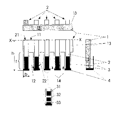
In Fig. 1 in a first embodiment a partial section of an SPR-sensor is
Zs shown. Therein, a plurality of strip-shaped light wave conductors 2
mutually arranged at defined distances are provided on a planar base 1 in
such a way that the leading faces 21, 22 are flush with the respective
sides 11, 12 of the planar base 1. Thereby each of the strip-shaped light
wave conductors 2 is provided in a section of said conductors with a thin
3o metal layer 3 which permits the excitation of surface plasmons, said
section being adapted to be brought into contact with fluid samples to be
analyzed, not shown in Fig. 1. In the example according to Fig. 1, the
starting point is a 4 "-silicon wafer used in the semiconductor techniques
into which initially the structures of a plurality of planar bases 1 have
3s been transferred and structurized. Thereby long and narrow rectangular
apertures are structurized in the wafer, said apertures forming the comb-
CA 02319429 2000-08-03
_6_
shaped recesses 14 after separation shown in Fig. 1. A mask which, in
the example, is used to this end has to be shaped to such a geometry that
the resulting comb-shaped structures, after having been separated, can be
submerged in micro-titer plates of a 1536 format (32x48 cavities). It is
s evident that only a section thereof is shown in Fig. 1. In order to ensure a
strength as high as possible for the single bases 1, a silicon wafer has
been selected having a crystal orientation (110) that permits to structurize
rectangular spaces with right angular edges at least at two edges.
Subsequently, the structurized wafer of the example is coated with Si02
io by way of a PE-CVD process. This Si02-layer is adapted as an optical
buffer between the arranged light wave conductors 2 and the Si-
substrate.
The light wave conductors according to Fig. 1 consist of a
siliconoxynitride layer of, for example, a thickness of about lOpm. The
is light wave conductors 2 are shaped, according to the scope of the present
invention, by a conventional dry etching procedure of the
siliconoxynitride layer in such a way that parallel stripes result having a
width of between 10 pm to 2000 ~.m and distances between 10 ~m and
5000 ~.m.
ao Furthermore, it is feasible within the scope of the invention to vary the
last mentioned sequence of structurizing in such a way that, on a non-
structurized Si-wafer, initially all the coatings mentioned are applied to
the entire surface of the wafer and, subsequently thereto, the comb-
shaped structure as shown in Fig. 1 is produced by employing the known
as selective structurizing procedures. In Fig. 1 a there is shown a plan view
of the structures, obtained in the above manner, along the plane X-X of
Fig. 1.
Furthermore, it lies within the scope of the invention to manufacture the
light wave conductor 2 of a polymer that can be hardened by the effect of
3o UV-light. To this end a liquid polymer, for example, PMMA,
polycarbonate, UV-hardened adhesives or silico-polymers (cyclotene or
ORMOCERE) is sputtered upon the wafer or embedded by casting on
the same. The structurizing of the light wave conductor is performed by
known photolithographic methods under use of a respectively prepared
3s mask. The exposed areas are cross-linked and hardened by UV-radiation,
CA 02319429 2000-08-03
- 7 _
whereas the unexposed areas are removed while developed so that the
exposed areas remain as light wave conductors 2.
The light wave conductor 2, in the most cases, has to be designed of
square cross-section, whereby departures due to manufacturing
s conditions may occur. The cross-section in the example according to Fig.
2 is about 190 ~m x 190 ~.m, the width b_ of the fingers f is about S50 -
600 Vim, whereby the light wave conductors 2 have to be centrally
arranged on the fingers f.
Such a dimensioning ensures an adaptation as far as possible to the light
io conducting fibers, which will be referred to in more detail in the
following, of the presently used diameters of 200 Vim. The Iengthh of the
sections comprising the fingers f is 5 mm in the example.
Under the condition that the optical refractive number of the base 1
material is lower than the refractive number of the polymer to be
is deposited, and that said material is not absorbing, the present example
according to Fig. 2 can do without an additional and prior application of
an optical buffer layer 13, as required in Fig. 1.
There can also be used different polymers that, for example, are brought
into the desired stripe shape by embossing or any other replication
Zo techniques, whereby the thickness of the remaining material has to lie
under the critical cut-off thickness in those parts in which no light has to
be conducted.
Subsequent to the above described structurizing of the strip-shaped light
wave conductors, the entire wafer in the two embodiments described up
Zs to here is protected by a cover coat except for those areas that are to
support the metal layer 3 capable of SPR. Thereafter, these uncovered
areas are coated with the metal sheet capable of SPR, for example, with a
thin gold layer by sputtering, and subsequent thereto the protective coat
is removed from the remaining covered areas.
3o Preferably the structures for the SPR-sensors on the wafers are produced
in such way that the comb-shaped structures are in mirror opposition to
one another before being separated. Before starting a subsequent sawing
process for separating the comb-structures and in order to protect the
light wave conductors 2 against fragments or the like, it is necessary to
3s passivate the light wave conductors 2 provided with the thin metal layers
3 adapted for exciting the surface plasmons. To this end a thick
CA 02319429 2000-08-03
_ g _
protective coating is applied. Then a separation process follows, for
example, by sawing, so that the desired comb-structures are obtained and
the leading faces 21, 22 are produced, said leading faces 21, 22 being
adapted to couple-in and couple-out, respectively, light.
s Depending on which technology is being used for providing the desired
comb-shaped recesses in the base body 1, said recesses 14 can be
manufactured before or after the application of said metal layer 3.
In the examples according to Fig. 1 and 2, said application is carried out
subsequently at least on those areas of the light wave conductor 2 that are
io formed by the leading faces 22 in the range of the metal layer 3. The
application of the reflecting coat 4 can be achieved, for example, by a
new coating process, for example, by sputtering of an aluminum layer or
a silver layer. To this end and before the separation process, the wafer is
provided with a protective coat over its entire surface, said protective
is coat ensuring that the structures 2, 3 that have been applied before, are
not contaminated during the end portions are being mirror coated. The
protective coat is removed after mirror coating.
In the examples according to Fig. 1 and 2, the single SPR-sensor areas
that are formed by the metal layers 3 are separated from one another by
Zo the comb-shaped recesses 14. Thus and, for example, by immersion into
an arrangement of complementarily distributed receptacles of a micro-
titer plate, each of the light wave conductors 2 can be associated to only
one sample.
In Fig. 3a a perspective view of an SPR-sensor according to Fig. 1 or 2 is
Zs shown. In order to implement an array of sensors, a plurality of such
stripes are placed in a serially stacked arrangement. Offside the ranges
that are provided with a thin metal layer 3 enabling the excitation of the
surface plasmons, the stripes are held by a common holding means and
are spaced apart in such a manner that their space corresponds, for
3o example, to the space between the receptacles of a micro-titer plate
format preselectable at will. In this way arrays of SPR-sensors, adaptable
as desired, for example, 8x12 as shown in Fig. 3b, can be manufactured.
After assembly, such an array is advantageously embedded in a
polymeric casting by that area which is not provided with the metal layer
3s 3 capable of SPR, in order to give an additional support to the SPR
waveguide array, as indicated schematically in Fig. 3b by a polymeric
CA 02319429 2000-08-03
-9-
sealing block 6. For performing measurements, said SPR waveguide
array is brought into contact to a micro-titer plate that supports the
samples to be analyzed. Thereby, in order to obtain an optimal
measurement, the SPR waveguide array is inserted into the micro-titer
s plate 7 so far until the metal areas 3 capable of SPR are completely
wetted by a sample 8, as schematically shown in Fig. 4.
A further feasible arrangement of the SPR-sensors is indicated in Fig. S.
In this example the single SPR-sensors are spaced apart from one another
by the cell walls 71 which comprise a respective finger f of the
Io mentioned comb-structure. In this example an SPR-array according to
the principle of end-reflection is employed.
Furthermore, in the examples according to Fig. 4 and 5, an external light
conducting fiber 9 is shown that can be accurately positioned over the
respective leading faces of the light wave conductor 2 by use of an x,y
is displacement table.
Thereby, this light conducting fiber (9) couples-in light from a white
light radiation source (not shown in detail) into the respective light wave
conductor 2, and this light being passed to the excitation area of the
surface plasmons where it is subsequently reflected at the second mirror-
Zo coated leading face. After the guided light has passed the excitation area
for a second time after reflection, the light from the light wave conductor
2 is coupled-out via the leading face and passed into the common branch
of a not shown fiber branching element. From there, the light arnves in,
for example, a spectrometer (not shown) for spectral evaluation. The
as spectrometer control and the data collection is carried out computer
controlled by a PC.
Alternatively, the spectrum can be determined in that the SPR-array is
measured in transmission. Instead of the fiber branching element a
simple light conducting fiber 9 is used for coupling-in the light into the
30 light wave conductor 2. A second light conducting fiber is positioned at
the exit of the light wave conductor 2. Said second light conducting fiber
conducts the light to a diffraction-grating spectrometer. Such a
configuration can do without a mirror coating on the end face of the light
wave conductor 2. However, the interaction length, i. e. the effective
3s sensor length, is reduced by 50%. The signal is less distinct by that
CA 02319429 2000-08-03
- -10-
factor. On the other hand, two coupling sites have to be positioned so that
the expenditures for apparatus and adjustment are increased.
Depending on the used measuring and computing technique, it is also
feasible to associate a light conducting fiber 9 to each of the provided
s light wave conductors 2, thereby enabling a simultaneous evaluation of
all samples present.
Two further embodiments, illustrated in Fig. 6a and 6~ are designed in a
way that the means separating the detection ranges of the single thin
metal layers 3 from one another are constituted by cell walls 15
io connected to the planar base 1. Also in these embodiments both above
mentioned operation modes are possible. Thus, an embodiment
according to Fig. 6a is adapted for an in-line operation, whereas an
embodiment according to Fig. 6.~ for the reflection mode operation by
providing a mirror-coating 4.
is In Fig. 6c there is indicated how an SPR-sensor array can be
manufactured by a multiple arrangement similar to the stacked
arrangement, described in Fig. 3~, of single lines supporting a plurality
of SPR-sensors according to Fig. 6a.
The invention is not restricted to the represented examples. In general, it
Zo is essential that the planar bases 1 are used that are provided with
substantially plane light wave conductors exhibiting, in a sample
detection area, at least one respective metal layer 3 capable of SPR that
constitutes one respective sample detection area which can be brought
into contact with a sample. It also lies within the scope of the invention
as to establish a communication between the areas capable of SPR and the
open bottoms of mutually spaced flow cells 16, Fig. 7, which have a
common inflow 17 and a common outflow 1 H. In particular, in such an
embodiment at least one of the provided flow cells can be used as
reference channels, for example, to compensate for temperature
3o variations.
When within the frame of the invention there is reference to at least one
two-dimensional measuring area, then thereby is to be understood that
the metal layer 3 provided as a sensor area can be subdivided into a
plurality of partial areas 31, 31, 33, as indicated in Fig. lb.
3s Furthermore, the inventional SPR-sensor can be employed in such a way
that initially one single sample is immobilized in the sensor areas 3. This
CA 02319429 2000-08-03
- 11 -
immobilization is adapted to prepare a chemically modified measuring
surface, and a further sample, preferably in solution, can enter into
interaction with said chemically modified surface. In the case of the
immobilized sample, this is frequently referred to as ligand, whereby the
s sample in solution is very often called receptor or analyt. Thus, the
interaction partners are, for example, ligand-receptor couples. Then, an
SPR-sensor according to the present example enables the simultaneous
measuring of a plurality of different samples (analyts).
All features disclosed in the specification, in the subsequent claims, and
Io in the drawing are substantial for the invention both, individually and in
any combination with one another.
CA 02319429 2000-08-03
- 12-
List of reference numerals
1 - planar base
11, 12 - (opposing) sides (of the planar base
1)
s 13 - buffer layer (coating)
14 - recesses
15 - cell walls
16 - flow cells
17 - inflow
io 18 - outflow
2 - light wave conductor
21, 22 - leading faces of the light wave conductor
2
3 - metal layer capable of SPR
31, 32, 33 - partial areas of the metal layer 3
is 4 - light-reflecting coat
6 - sealing block
8 - sample
9 - light conducting fiber
1 - width of the fingers f
ao f - fingers
h - length of fingers f
X-X - plane