Note: Descriptions are shown in the official language in which they were submitted.
CA 02319570 2000-08-03
Specification
Semiconductor Pressure Sensor and
Method of Manufacturing the Same
Technical Field
The present invention relates to a
semiconductor pressure sensor for measuring a pressure
by utilizing the piezoresistive effect of a
semiconductor, and a method of manufacturing the same.
Background Art
Among various types of pressure sensors, a
semiconductor pressure sensor which utilizes the
piezoresistive effect of a semiconductor is compact,
lightweight, and highly sensitive, and is accordingly
widely used in applications such as industrial
instrumentation field and medical field. In such a
semiconductor pressure sensor, a strain gauge with a
piezoresistive effect is formed on a semiconductor
diaphragm. The strain gauge is deformed by a pressure
applied to the diaphragm, and a change in resistance of
the strain gauge caused by the piezoresistive effect is
detected, thereby measuring the pressure. The diaphragm
is formed by engraving one surface of a semiconductor
wafer by etching. The thickness of the diaphragm
largely influences the characteristics of the
semiconductor pressure sensor. Accordingly, the
thickness of the diaphragm must be controlled precisely.
- 1 -
CA 02319570 2000-08-03
In a conventional manufacturing method, however, the
etching time and temperature are difficult to control,
making it very difficult to control the thickness of the
diaphragm and its uniformity at high precision.
A semiconductor pressure sensor has been
proposed in which an etching stopper layer made of an
insulator or the like is formed in a semiconductor
substrate, and the semiconductor substrate is etched to
the etching stopper layer, thereby precisely controlling
l0 the thickness of the diaphragm (Japanese Patent
Publication No. 59-38744). Fig. 4 is a sectional view
of the conventional semiconductor pressure sensor
disclosed in Japanese Patent Publication No. 59-38744.
This semiconductor pressure sensor is comprised of a
single-crystal Si layer 11 serving as a base, an Si02
layer 12 formed on the single-crystal Si layer 11, a
single-crystal Si layer 13 formed on the Si02 layer 12,
a diaphragm 14 formed by etching that portion of the
single-crystal Si layer 11 which corresponds to the
pressure-sensitive region by using the Si02 layer 12 as
an etching stopper layer, and a strain gauge (not shown)
with a piezoresistive effect formed on the surface of
the single-crystal Si layer 13.
In the semiconductor pressure sensor shown in
Fig. 4, the diaphragm 14 undesirably has temperature
characteristics due to a difference in coefficient of
thermal expansion between the Si layer 13 and Si02 layer
- 2 -
CA 02319570 2000-08-03
12. Also, at a diaphragm edge portion 16, cracking
occurs in the SiOz layer 12 more fragile than Si due to
deflection of the diaphragm 14. This cracking extends
to the Si layer 13 to finally break the diaphragm 14.
Even if the exposed Si02 layer 12 is removed after
etching the Si layer 11, since the Si02 layer 12 remains
in the diaphragm edge portion 16, cracking still occurs
in an interface between the Si layer 13 and Si02 layer
12.
The present invention has been made in order
to solve these problems, and has as its object to
provide a semiconductor pressure sensor in which the
temperature characteristics of a diaphragm can be
improved and the strength of a diaphragm edge portion
can be increased, and a method of manufacturing the same.
Disclosure of Invention
In order to achieve the above object, the
present invention comprises a first semiconductor layer
forming a base, an insulating layer formed on the first
semiconductor layer, a second semiconductor layer formed
on the insulating layer and having a diaphragm portion
constituting a pressure-sensitive region, and a recess
formed in the pressure-sensitive region to extend
through the first semiconductor layer and the insulating
layer to have a predetermined depth reaching the second
semiconductor layer. Hence, the insulating layer does
not remain on the diaphragm portion and a diaphragm edge
- 3 -
CA 02319570 2000-08-03
portion.
The present invention also comprises the steps
of forming a three-layered structure consisting of a
first semiconductor layer forming a base, an insulating
layer formed on the first semiconductor layer, and a
second semiconductor layer formed on the insulating
layer and having a pressure-sensitive region, etching
the first semiconductor layer corresponding to the
pressure-sensitive region by using the insulating layer
as an etching stopper layer, thereby exposing the
insulating layer, removing the exposed insulating layer,
and etching the second semiconductor layer by a
predetermined amount by using the remaining insulating
layer as a mask, thereby forming a diaphragm portion at
the pressure-sensitive region.
In the present invention, the depth of the
recess formed in the second semiconductor layer has an
upper allowable limit of ten-odd ,um.
According to one arrangement of the present
invention, the second semiconductor layer has a
thickness of 30 ~Cm and the recess formed in the second
semiconductor layer has a depth of 5 ,ccm to 10 ,um.
According to one arrangement of the present
invention, the first and second semiconductor layers are
made of n-type single-crystal Si and the insulating
layer is made of SiOZ.
One arrangement of the present invention
- 4 -
CA 02319570 2000-08-03
comprises at least one strain gauge formed on the
diaphragm portion of the second semiconductor layer.
Brief Description of Drawings
Fig. 1 is a sectional view of a semiconductor
pressure sensor according to an embodiment of the
present invention;
Fig. 2 shows plan and bottom views of the
semiconductor pressure sensor of Fig. 1;
Fig. 3 shows sectional views of the steps in a
method of manufacturing the semiconductor pressure
sensor of Fig. 1; and
Fig. 4 is a sectional view of a conventional
semiconductor pressure sensor.
Best Mode of Carryout Out the Invention
An embodiment of the present invention will be
described in detail with reference to the accompanying
drawings. Fig. 1 is a sectional view of a semiconductor
pressure sensor according to the embodiment of the
present invention, Fig. 2(A) is a plan view of the
semiconductor pressure sensor of Fig. 1, and Fig. 2(B)
is a bottom view of the semiconductor pressure sensor of
Fig. 1.
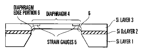
This semiconductor pressure sensor is
comprised of an n-type single-crystal Si layer 1 serving
as a base, an SiOz layer 2 formed on the n-type
single-crystal Si layer l, an n-type single-crystal Si
layer 3 formed on the Si02 layer 2, a diaphragm 4 formed
- 5 -
CA 02319570 2000-08-03
by etching that portion of the n-type single-crystal Si
layer 1 which corresponds to a pressure-sensitive region
to the Si02 layer 2 by using the Si02 layer 2 as an
etching stopper layer, removing the exposed Si02 layer 2,
and etching the pressure-sensitive region of the n-type
single-crystal Si layer 3 by a predetermined amount, and
strain gauges 5 with a piezoresistive effect formed on
the pressure-sensitive region of the n-type
single-crystal Si layer 3.
A method of manufacturing this semiconductor
pressure sensor will be described with reference to
Fig. 3. First, as shown in Fig. 3(A), an SOI (Silicon
On Insulator) wafer constituted by the n-type
single-crystal Si layer 1, the SiOz layer 2 with a
thickness of about 0.5 Vim, and the n-type
single-crystal Si layer 3 is prepared. To fabricate
this SOI wafer, an SIMOX (Separation by IMplanted
OXygen) technique of forming an SiOz layer by implanting
oxygen into an Si substrate, an SDB (Silicon Direct
Bonding) technique of bonding two Si substrates, or
other methods may be used.
The n-type single-crystal Si layer 3 is
polished to a predetermined thickness (for example,
~m ) by a polishing method called CCP (Computer
25 Controlled Polishing) or the like in order to planarize
and thin it. Alternatively, an n-type single-crystal Si
layer 3 having a predetermined thickness may be formed
- 6 -
CA 02319570 2000-08-03
on the Si02 layer 2 by epitaxy. An Si02 film or resist
(not shown) is formed on the lower surface of the SOI
wafer formed in this manner, and an opening is formed in
that portion of the SiOZ film or resist which
corresponds to a pressure-sensitive region (a region
where the diaphragm 4 is to be formed). By using the
Si0 film or resist patterned in this manner as a
2
diaphragm forming etching mask, the n-type
single-crystal Si layer 1 is dipped in a solution of KOH
or TMAH, thereby etching the n-type single-crystal Si
layer 1 (Fig. 3(B)). Etching progresses gradually at
the opening described above, and stops automatically
upon reaching the Si02 layer 2.
Subsequently, the SiOz layer 2 is etched with
a solution of HF or the like by using the n-type
single-crystal Si layer 1 as an etching mask, to remove
the Si02 layer 2 exposed by etching the Si layer 1
(Fig. 3(C)). By using the SiOz layer 2 as an etching
mask, the n-type single-crystal Si layer 3 is etched
with a solution of KOH or TMAH (Fig. 3(D)). The etching
depth is controlled to a predetermined small amount
(about 5 ~m to 10 Vim} by time management.
The diaphragm 4 is formed in this manner.
Since the etching amount of the n-type single-crystal Si
layer 3 is as very small as about 5 ~m to 10 ~cm and
the thickness of the n-type single-crystal Si layer 3
does not vary with etching of ten-odd ~cm or less, the
CA 02319570 2000-08-03
diaphragm.4 can be formed with a uniform thickness. The
strain gauges (piezoresistive regions) 5 made of p-Si
are formed on the upper surface of the n-type
single-crystal Si layer 3 by impurity diffusion or ion
implantation (Fig. 3(E)).
Successively, an SiOz layer (not shown) is
formed on the upper surface of the n-type single-crystal
Si layer 3, and contact holes are formed in the SiOz
layer on the strain gauges 5. After that, A1 electrodes
(not shown) are formed on the contact hole portions by
vapor deposition in order to obtain electrical contact
with the strain gauges 5. Then, the manufacture of the
semiconductor pressure sensor is ended.
As described above, that portion of the n-type
single-crystal Si layer 1 which corresponds to the
pressure-sensitive region is etched from its lower
surface to the SiOz layer 2 by using the Si02 layer 2 as
the etching stopper layer, then the SiOz layer 2 exposed
by this etching is removed, and the pressure-sensitive
region of the n-type single-crystal Si layer 3 is etched
by a very small amount, so the Si02 layer 2 will not
remain on the diaphragm 4 and a diaphragm edge portion 6.
As a result, the temperature characteristics of the
diaphragm 4 can be improved, and the strength of the
diaphragm edge portion 6 can be increased.
Although anisotropic etching utilizing the
crystallographic axis etching characteristics of
_ g _
CA 02319570 2000-08-03
single-crystal Si is performed in this embodiment,
isotropic etching may be performed instead. Dry etching
may be performed in place of wet etching as in this
embodiment.
Industrial Applicability
The semiconductor pressure sensor according to
this invention is suitable as a pressure sensor used in
industrial instrumentation field and medical field.
_ g _