Note: Descriptions are shown in the official language in which they were submitted.
CA 02319729 2000-08-O1
WO 99/42796 PCT/US99/03481
Birefringence Measurement System
Technical Field
This application relates to a system and method for precise measurement
of linear birefringence properties of a transparent sample.
Background
Many important optical materials exhibit birefringence. Birefringence
means that different linear polarizations of light travel at different speeds
through
the material. These different polarizations are most often considered as two
components of the polarized light, one being orthogonal to the other.
Birefringence is an intrinsic property of many optical materials, and may
also be induced by external forces. Retardation or retardance represents the
integrated effect of birefringence acting along the path of a light beam
traversing
the sample. If the incident light beam is linearly polarized, two orthogonal
components of the polarized light will exit the sample with a phase
difference,
called the retardance. The fundamental unit of retardance is length, such as
nanometers (nm). It is frequently convenient to express retardance in units of
phase angle (waves, radians, or degrees) which is proportional to the
retardance
(nm) divided by the wavelength of the light (nm). An "average" birefringence
for a
sample is sometimes computed by dividing the measured retardation magnitude
by the thickness of the sample.
The two orthogonal polarization components described above are parallel
to two orthogonal axes, which are determined by the sample and are called the
CA 02319729 2000-08-O1
WO 99/42796 PCT/US99/03481
2
"fast axis" and the "slow axis." The fast axis is the axis of the material
that aligns
with the faster moving component of the polarized light through the sample.
Therefore, a complete description of the retardance of a sample along a given
optical path requires specifying both the magnitude of the retardance and the
relative angular orientation of the fast (or slow) axis.
The need for precise measurement of birefringence properties has
become increasingly important in a number of technical applications. For
instance, it is important to specify and control the residual linear
birefringence
(hence, the attendant induced retardance) in optical elements used in high
precision instruments employed in semiconductor and other industries. The
optics industry thus has a need for a highly sensitive instrument for
measuring
linear birefringence in optical components. This need has been largely unmet,
especially with respect to measurements of low levels of retardance.
Summary of the invention
The present invention is directed to a practical system and method for
precisely measuring low-level birefringence properties of optical materials.
The
retardance magnitude and orientation of the fast axis are precisely
calculated.
The system permits multiple measurements to be taken across the area of a
sample to detect and graphically display variations in the retardance across
the
sample area.
In a preferred embodiment, the system incorporates a photoelastic
modulator for modulating polarized light that is then directed through a
sample.
The beam propagating from the sample is separated into two parts. These
CA 02319729 2000-08-O1
WO 99/42796 PC'T/US99/03481
3
separate beam parts are then analyzed at different polarization directions,
detected, and processed as distinct channels. The detection mechanisms
associated with each channel detect the light intensity corresponding to each
of
the two parts of the beam. This information is employed in an algorithm for
calculating a precise, unambiguous measure of the retardance induced by the
sample and the orientation of the fast axis.
As one aspect of this invention, the system includes a beam-splitting
member and detector arrangement that permits splitting the beam into two parts
with minimal contribution to the retardance induced in the beam. Moreover, the
presence of any residual birefringence in the optical system {such as may
reside
as static birefringence in the photoelastic modulator or in any of the optical
components of the system) is accounted for in a number of ways. For example,
certain of the system components are arranged or mounted to minimize the
chance that strain-induced birefringence may be imparted into the element. A
reliable calibration technique is also provided.
The system permits the low-level birefringence measurements to be taken
at any of a plurality of locations across the area of the sample. The
measurements are compiled in a data file and graphically displayed for quick
analysis.
In one embodiment of the invention, the optical components of the system
are arranged to measure the birefringence properties of a sample that is
reflectively coated on one side, thereby permitting measurement of
birefringence
properties even though the sample is not completely fight transmissive.
CA 02319729 2000-08-O1
WO 99/42796 PCT/US99/03481
4
Other advantages and features of the present invention will become clear
upon study of the following portion of this specification and drawings.
Brief Description of Drawings
Fig. 1 is a diagram of a preferred embodiment of the present system
showing the preferred arrangement of the optical components.
Fig. 2 is a block diagram of the processing components of the present
system.
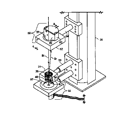
Fig. 3 is a perspective view of detection and beam-splitting components of
the system.
Fig. 4 is a cross-sectional view of one of the detector assemblies of the
system.
Fig. 5 is a perspective view of the primary components of a photoelastic
modulator that is incorporated in the present system.
Fig. 6 is a drawing depicting a graphical display provided by the system of
the present invention.
Fig. 7 is a diagram of an alternative embodiment of the present invention.
Fig. 8 is a graph that plots, for a selected retardance, the oscillation
amplitude of the polarization modulator against a number of source-light
wavelengths, for a polarization modulator that employs a preferred type of
optical
element.
CA 02319729 2000-08-O1
WO 99/42796 PCTNS99/03481
Fig. 9 is a graph, based in part on the data shown in Fig. 8, that represents
a correction factor that may be applied to convert the retardance value of an
optical-material sample as measured at one source-fight wavelength to the
retardance value that would occur in the sample at another source-light
5 wavelength.
Fig. 10 is a graph that plots, for a selected retardance, the oscillation
amplitude of the polarization modulator against a number of source-light
wavelengths, for a polarization modulator that employs an alternative type of
optical element.
Fig. 11 is a another graph, like Fig. 9, that represents a correction factor
that may be applied to convert the retardance value of an optical-material
sample
as measured at one source-light wavelength to the retardance value that would
occur in the sample at another source-light wavelength.
Best Modes for Carrying Out the Invention
The diagram of Fig. 1 depicts the primary optical components of a system
made in accordance with the present invention. The components include a HeNe
laser as a light source 20 that has a wavelength of 632.8 nanometers (nm). The
beam "B" emanating from the source has a cross sectional area or "spot size"
of
approximately 1 millimeter (mm).
The source light beam "B" is directed to be incident on a polarizer 22 that
is oriented with its polarization direction at +45° relative to a
baseline axis. A
high-extinction polarizer, such as a Glan-Thompson calcite polarizer, is
preferred.
CA 02319729 2000-08-O1
WO 99/42796 PCT/US99/03481
6
It is also preferred that the polarizer 22 be secured in a precision,
graduated
rotator.
The polarized light from the polarizer 22 is incident on the optical element
25 of a photoelastic modulator 24 (Figs. 1 and 5). In a preferred embodiment,
the
photoelastic modulator (hereafter referred to as a "PEM~) is one manufactured
by
Hinds Instruments, Inc., of Hillsboro, Oregon, as a low birefringence version
of
Model PEM-90 I/FS50. It is noteworthy here that although a PEM is preferred,
one could substitute other mechanisms for modulating the polarization of the
source light.
The PEM has its birefringent axis oriented at 0° and is controlled
by a
controller 84 that imparts an oscillating birefringence to the optical element
25,
preferably at a nominal frequency of 50 kHz. In this regard, the controller 84
drives two quartz transducers 29 between which the optical element 25 is
bonded
with an adhesive.
The oscillating birefringence of the PEM introduces a time-varying phase
difference between the orthogonal components of the polarized light that
propagates through the PEM. At any instant in time, the phase difference is
the
retardation introduced by the PEM. The retardation is measurable in units of
length, such as nanometers. The PEM is adjustable to allow one to vary the
amplitude of the retardation introduced by the PEM. In the case at hand, the
retardation amplitude is selected to be 0.383 waves (242.4 nm).
The beam of light propagating from the PEM is directed through the
transparent sample 26. The sample is supported in the path of the beam by a
CA 02319729 2000-08-O1
WO 99/42796 PCT/US99/03481
7
sample stage 28 that is controllable for moving the sample in a translational
sense along orthogonal (X and Y) axes. The stage may be any one of a number
of conventional designs such as manufactured by THK Co. Ltd., of Tokyo, Japan
as model KR2602 A-250. As will become clear, the motion controllers of the
sample stage 28 are driven to enable scanning the sample 26 with the beam to
arrive at a plurality of retardance and orientation measurements across the
area
of the sample.
The sample 26 will induce retardance into the beam that passes through it.
It is this retardance value that is determined in accordance with the
processing
provided by the present invention, as explained more below. The present system
is especially adapted to determine low levels of retardance. Low retardance
levels are determined with a sensitivity of less than t 0.01 nm.
In order to obtain an unambiguous measure of the sample-induced
retardance, the beam "Bi" that passes out of the sample is separated into two
parts having different polarization directions and thereby defining two
channels of
information for subsequent processing.
Turning first to the preferred mechanism for separating the beam "Bi,"
there is located in the path of that beam (hereafter referred to as the
incidence
path) a beam-splitting mirror 30. Part "B1" of the beam "Bi" passes completely
through the beam-splitting mirror 30 and enters a detector assembly 32 for
detection.
CA 02319729 2000-08-O1
WO 99/42796 PCT/US99/03481
8
Fig. 3 depicts a preferred mechanism for supporting the beam-splitting
mirror 30. In particular, the mirror 30 is seated in the central aperture of a
housing 31 that is rigidly supported by an arm 33 to a stationary vertical
post 36.
The post 36 is employed for supporting all of the optical components of the
system so that the paths of the light are generally vertical.
The diameter of the mirror 30 is slightly less than the diameter of the
housing aperture. The aperture is threaded except for an annular shoulder that
projects into the lowermost end of the aperture to support the periphery of
the
flat, round mirror 30. A retainer ring 40 is threaded into the aperture to
keep the
mirror in place in the housing 31 against the shoulder.
In a preferred embodiment, care is taken to select and mount the mirror 30
so that substantially no stress-induced birefringence is introduced into the
mirror.
In this regard, the mirror is preferably made of Schott Glass type SF-57
glass.
This glass has an extremely low (near zero) stress-optic coefficient. The
retainer
ring 40 is carefully placed to secure the mirror without stressing the glass.
Alternatively, flexible adhesive may be employed to fasten the mirror. No
setscrews or other stress-inducing mechanisms are employed in mounting the
mirror.
It is noteworthy here that, although a beam-splitting mirror is preferred,
one can substitute other mechanisms (such as a flipper mirror arrangement) for
separating the beam "Bi" into two parts.
CA 02319729 2000-08-O1
WO 99/42796 PCT/US99/03481
9
The part of the beam "B1" that passes through the mirror 30 enters the
detector assembly 32 (Fig. 1 ), which includes a compact, Glan-Taylor type
analyzer 42 that is arranged such that its polarization direction is at -
45° from the
baseline axis. From the analyzer 42, the beam "B1" enters a detector 44, the
particulars of which are described more below.
The reflective surface 35 of the beam-splitting mirror 30 (Fig. 3) faces
upwardly, toward the sample 26. The mirror is mounted so that the incidence
path (that is, the optical path of the beam "Bi" propagating from the sample
26) is
nearly normal to the reflective surface 35. This orientation is preferred for
substantially eliminating retardance that would otherwise be introduced by an
optical component that is called on to redirect the path of the beam by more
than
a few degrees.
Fig. 1 shows as "A" the angle made between the beam "Bi" travelling along
the incidence path and the beam part "Br" that is reflected from the mirror
30.
Angle "A" is shown greatly enlarged for illustrative purposes. In a preferred
embodiment, this angle is greater than 0° but less than 10°.
Most preferred is an
angle "A" of under 5°.
The reflected part of the Beam "Br" is incident upon another detector
assembly 50. That assembly 50 is mounted to the post 36 (Fig. 3) and
configured in a way that permits the assembly to be adjacent to the incident
beam "Bi" and located to receive the reflected beam "Br." More particularly,
the
assembly 50 includes a base plate 52 that is held to the post 36 by an arm 54.
As seen best in Fig. 4, the base plate includes an inner ring 57 that is
rotatably
CA 02319729 2000-08-O1
WO 99/42796 PCT/US99/03481
mounted to the base plate and has a large central aperture 56 that is
countersunk
to define in the bottom of the plate 52 an annular shoulder 58.
The detector components are compactly integrated and contained in a
housing 60 that has a flat front side 62. The remainder of the side of the
housing
5 is curved to conform to the curvature of the central aperture 56 of the base
plate
52. Moreover, this portion of the housing 60 includes a stepped part 64 that
permits the curved side of the housing to fit against the base plate 52 and be
immovably fastened thereto.
A sub-housing 70 is fastened inside of the detector components housing
10 60 against the flat side 62. The sub-housing 70 is a generally cylindrical
member
having an aperture 72 formed in the bottom. Just above the aperture 72 resides
a compact, Glan-Taylor type analyzer 74 that is arranged so that its
polarization
direction is 0°, parallel with that of the PEM 24.
Stacked above the analyzer 74 is a narrow-band interference filter 77 that
permits passage of the polarized laser light but blocks unwanted room light
from
reaching a detector 76. The detector is preferably a photodiode that is
stacked
above the filter. The photodiode detector 76 is the preferred detection
mechanism and produces as output a current signal representative of the time
varying intensity of the received laser fight. With respect to this assembly
50, the
laser light is that of the beam "B2," which is the reflected part "Br" of the
beam
that propagated through the sample 26.
CA 02319729 2000-08-O1
WO 99!42796 PCT/US99/03481
11
The photodiode output is delivered to a preamplifier carried on an
associated printed circuit board 78 that is mounted in the housing 60. The
preamplifier 75 (Fig. 2) provides output to a phase sensitive device
(preferably a
lock-in amplifier 80) in the form of a low-impedance intensity signal VAS, and
a DC
intensity signal Vp~, which represents the time average of the detector
signal.
It is noteworthy here that the other detector assembly 32 (Fig. 3) to which
is directed the non-reflected part "B1" of the beam "Bi" is, except in two
respects,
the same construction as the just described assembly 50. As shown in Fig. 3,
the
detector assembly 32 is mounted to the post 36 in an orientation that is
generally
inverted relative to that of the other detector assembly 50. Moreover, the
analyzer 42 of that assembly 32 is arranged so that its polarization direction
is
oblique to the polarization direction of the analyzer 74 in the other detector
assembly 50. Specifically, the analyzer 42 is positioned with its polarization
direction at -45°. The preferred analyzer position is established by
rotating the
detector assembly via the inner ring 57 discussed above.
The photodiode of detector assembly 32 produces as output a current
signal representative of the time varying intensity of the received laser
fight. With
respect to this assembly 32, the laser light is that of the beam "B1," which
is the
non-reflected part of the beam "Bi" that propagated through the sample 26.
The photodiode output of the detector assembly 32 is delivered to a
preamplifier 79, which provides its output to the lock-in amplifier 80 (Fig.
2) in the
form of a low-impedance intensity signal VAS, and a DC intensity signal Voc,
which represents the time average of the detector signal.
CA 02319729 2000-08-O1
WO 99/42796 PCT/US99/03481
12
In summary, the lock-in amplifier 80 is provided with two channels of input:
channel 1 corresponding to the output of detector assembly 32, and channel 2
corresponding to the output of detector assembly 50. The intensity information
received by the lock-in amplifier on channel 1 -because of the arrangement of
the -45° analyzer 42- relates to the 0° or 90° component
of the retardance
induced by the sample 26. The intensity information received on channel 2 of
the
lock-in amplifier 80 -as a result of the arrangement of the 0° analyzer
74- relates
to the 45° or -45° component of the retardance induced by the
sample. As
explained below, this information is combined in an algorithm that yields an
unambiguous determination of the magnitude of the overall retardance induced
in
the sample (or a location on the sample) as well as the orientation of the
fast axis
of the sample (or a location on the sample).
The lock-in amplifier 80 may be one such as manufactured by EG&G Inc.,
of Wellesley, Massachusetts, as model number 7265. The lock-in amplifier takes
as its reference signal 82 the oscillation frequency applied by the PEM
controller
84 to the transducers 29 that drive the optical element 25 of the PEM 24. The
lock-in amplifier 80 communicates with a digital computer 90 via an RS232
serial
interface.
For a particular retardance measurement, such as one taken during the
scanning of several locations on a sample, the computer 90 obtains the values
of
channel 1. The computer next obtains the values of channel 2. The intensity
signals on the detectors in channels 1 and 2 are derived as follows:
CA 02319729 2000-08-O1
WO 99/42796 PCT/US99/03481
13
I~h, =1 + cos(4p) sine ~ cos0 - cos2 ~ cosh + cos(2p) sin 8 sin0
eqn. (1 )
I~h2 =1 + sin(4p) sine ~ cos0 + sin(2p) sin 8 sin 0
where D is the PEM's time varying phase retardation; b is the magnitude of the
sample's retardance; and p is the azimuth of the fast axis of the sample's
retardance. The Mueller matrix for a linearly birefringent sample (8, p) used
in the
derivation has the following form:
0 0 0
s2 s2 . . s2
1 cos(4~p)~sin - +cos - sm(4~p)~s~n - -sin(2~p)~sin(s)
2 2 2
s2 . s2 s2
1 sin (4~p) sin Z cos (4 ~p) ~s~n 2 + cos ~ cos (2 ~p) sin (s )
1 sin(2~p)~sin(s) -(cos(2~p)~sin(s)) cos(s)
In equations (1 ), sin0 (D= Aosinwt, where w is the PEM's modulating
frequency; ~ is the maximum peak retardance of the PEM) can be expanded
with the Bessel functions of the first kind:
sin 0 = sin(Do sin(~t)) _ ~ 2J2k+, (~o ) sin((2k + 1)~t) eqn. (2)
2k+1
where k is either "0" or a positive integer; and J2k+, is the (2k+1 )th order
of the
CA 02319729 2000-08-O1
WO 99/42796 PCT/US99/03481
14
Bessel function. Similarly, cos0 can be expanded with the even harmonics of
the
Bessel functions:
cos0 = cosl~o sin(~cx)) = Jo (Do ) + ~ZJ2k (Do ) cos(~k)~c,~) eqn. (3)
2k
where Jo is the 0~' order of the Bessel function, and J2k is the (2k)th order
of the
Bessel function.
As seen from eqns. 1-3, it is preferable to determine the magnitude and
angular orientation of retardance using the signal at the PEM's first
harmonic.
The useful signal for measuring linear birefringence at the PEM's 2nd harmonic
is
modified by sin2(b/2), a value that is much smaller than sin8. The 1 F
electronic
signal on the detectors can be expressed in equation (4):
I~m,,F = sin b cos( 2 p)2J, (0 0 ) sin( wt)
1 ch2,lF = sin S sin( 2 p)2J1 (O o ) sin( Wit) eqn. (4)
As noted, the 1 F signal is determined using the lock-in amplifier 80 that is
referenced at the PEM's first harmonic. The lock-in amplifier will exclude the
contributions from all harmonics other than 1 F. The output from the lock-in
amplifier 80 for the two channels is:
I~hylF~= S cos( 2p)2J,(Do)~
Ich 2 ~1 F ~ _ ~ sin( 2 p ) 2 J, ( ~ o ) ~ eqn. (5)
using the approximation of sins = S for low-level linear birefringence; and ~2
results from the fact that the lock-in amplifier measures the r.m.s. of the
signal,
instead of the amplitude.
CA 02319729 2000-08-O1
WO 99/42796 PCT/US99/03481
All terms appearing at a frequency other than the PEM's first harmonic are
neglected in obtaining equations (5). The validity of equations (5) for
obtaining
the 1 F VAC signal is further ensured from the approximation that sin2(8/2) =
0
when 8 is small. This applies for low-level retardance of, for example, less
than
5 20 nm.
In order to eliminate the effect for intensity fluctuation of the light
source, or
variations in transmission due to absorption, reflection losses, or
scattering, the
ratio of the 1 F VAC signal to the Voc signal is used. (Alternatively, similar
techniques can be employed, such as dynamically normalizing the DC signal to
10 unity.) Exclusion of the cosh terms in equation (1 ) can severely affect
the Vpc
signal in channel i even though it has a minimal effect on the determination
of
the 1 F VAC signal using a high quality lock-in amplifier. The term
cos2(8/2)cos0 in
equation (1 ) is approximately equal to cos0 for small 8. As seen from
equation
(3), cos0 depends on Jo(Do), which is a "DC" term. Consequently, this DC term
15 should be corrected as in equations (7):
I~h,~lF~ 1-Jo(Do) 1 = R~,,, = g cos( 2p)
1 d~ ~ 2 J, (O o ) . ~ eqn. (7)
I~na~lF ~ 1 1 _
Id~ . 2J,(~o) ~ ~ R~hz = 8 sin( 2p)
where R~,t, and R~,,2 are experimentally determined quantities from the two
channels.
To correct the "DC" term caused by the cos0 term in channel 1, one
properly sets the PEM retardation so that Jo(~o) = 0 (when ~o = 2.405 radians,
or
CA 02319729 2000-08-O1
WO 99/42796 PCT/US99/03481
16
0.383 waves). At this PEM setting, the efficiency of the PEM for generating
the
1 F signal is about 90% of its maximum.
Finally, the magnitude and angular orientation of the linear birefringence is
expressed in equations (8):
p = 1 tari 1 R'~ or p = 1 ctg-' R'h
2 R~hy 2 R~h2 eqn. (8)
2
~R~hi ~ + ~R~t~2
These equations (8) are compiled in a program running on the computer
90 and used to determine the magnitude and orientation of the retardance at
any
selected point on the sample.
Equations (8) are specifically developed for small linear birefringence. The
approximation of sin8 = S used in deriving equations (8) has an error of ~1 %
for 8
= 20 nm when the light wavelength is at 632.8 nm. For any larger retardation,
sin8 should be used, instead of 8.
As noted above, best retardance measurement results are achieved when
one minimizes the residual birefringence present in the optical components of
the
system. To this end, the present system employs a PEM 24 (Fig. 5) that is
specially configured to eliminate residual birefringence that may be
attributable to
supporting the optical element 25 of the PEM in the housing 27 (shown in
dashed
lines of Fig. 5). The bar-shaped optical element is bonded at each end to a
transducer 29. Each transducer 29 is mounted to the PEM housing 27, as by
supports 23, so that the optical element is essentially suspended, thus free
from
CA 02319729 2000-08-O1
WO 99/42796 PCT/US99103481
17
any residual birefringence that may be attributable to directly mounting the
oscillating optical element 25 to the PEM housing 27.
Notwithstanding efforts such as the foregoing to eliminate residual
birefringence in the system components, the presence of at least some level of
residual birefringence is inevitable. In the present system, highly accurate
results
are obtained by correcting the results of equations 8 to account for any
remaining
residual birefringence in the system, which residual may be referred to as the
system offset. In practice, residual birefringence in the optical element of
the
photoelastic modulator and in the beam-splitting mirror substrate can induce
errors in the resulting measurements. Any such errors can be measured by first
operating the system with no sample in place. A correction for the errors is
made
by subtracting the error values for each channel.
The system offset is obtained by making a measurement without a sample
in place. The results from both channels 1 and 2 are the system offsets at
0° and
45° respectively:
0
Ro __ l~n~<1F) _So(p=0)
~m 2 J 1 ( ~ o ) 1 am eqn, (9)
0
R o I ch 2 ~l F )
~hz - 2J~(Oo)I~z 4
where the superscript "°" indicates the absence of a sample. The
equation
bearing the term p = 0 corresponds to channel 1 (the -4.5° analyzer
42). The
equation bearing the term p = ~c/4 corresponds to channel 2 (the 0°
analyzer 74).
The system offsets are corrected for both channels when a sample is measured.
The system offsets for channels 1 and 2 are constants (within the measurement
CA 02319729 2000-08-O1
WO 99/42796 PCT/US99/03481
18
error) at a fixed instrumental configuration. Barring any changes in the
components of the system, or in ambient pressure or temperature, the system
should remain calibrated.
In principle, this procedure will provide a method of self calibration of the
system. It is, however, prudent to compare the system measurement of a sample
with the measurement obtained using other methods.
One such calibration sample may be provided by a compound zero-order
waveplate. The compound waveplate comprises two multiple-order waveplates
(e.g., quartz) or two zero-order waveplates (e.g., mica) selected to have a
very
small retardance difference between them (e.g., less than 0.03 wavelengths).
They would be combined with their axes at right angles so that the retardance
of
one is subtracted from the other to produce the sought-after low-level
retardance,
compound zero-order waveplate(s) for use in calibration. Such a configuration
will provide a uniform retardance across the surface with a low temperature
coefficient of retardance.
If the components of the present system are correctly set up, the
magnitude of the measured, sample-induced retardance will be independent of
the sample's angular orientation. This angular independence may be lost if: (1
)
the polarization directions of the polarizer 22 and analyzers 42, 74 are not
precisely established, and (2) the maximum peak retardance of the PEM is not
precisely calibrated. What follows is a description of correction techniques
for
eliminating the just mentioned two sources of possible "angular dependence"
errors.
CA 02319729 2000-08-O1
WO 99/42796 PCT/US99/03481
19
As respects the precise establishment of the polarization directions of the
polarizer 22 and analyzers 42, 74, the correction technique applied to the
polarizer 22 involves the following steps:
1. With the PEM operating, approximately orient the polarizer 22 and the
channel 1 analyzer/detector assembly 32 at 45° and -45°,
respectively.
2. Rotate the polarizer 22 in fine increments while monitoring the 2F (100
kHz) lock-in amplifier signal from channel 1. When the 2F signal reaches
"0" (practically, the noise level at the highest lock-in amplifier sensitivity
possible), read precisely the angle on the polarizer rotator.
3. Rotate the polarizer 22 by precisely 45°, which is the correct
position
for the polarizer.
4. Once the position of the polarizer 22 is correctly established, turn off
the
PEM and rotate analyzer/detector assembly 32 while monitoring the lock-
in amplifier's Vp~ signal from channel 1. When the minimum Vp~ signal is
achieved, the position of analyzer/detector assembly 32 is set correctly.
5. Once the position of the polarizer 22 is correctly established, rotate
analyzer/detector assembly 50 while monitoring the lock-in amplifier's 2F
(100 kHz) signal from channel 2. When this 2F signal reaches "0"
(practically, the noise level at the highest lock-in amplifier sensitivity
possible), the position of analyzer/detector assembly 50 is set correctly.
As respects the calibration of the PEM, the following technique may be
employed:
1. Set the channel 1 analyzer/detector assembly 32 at -45° when the
polarizer 22 is at +45°.
2. Record the Vp~ signals with a precision voltmeter while the PEM
retardance is changed in the vicinity of, for example, ~10% of the selected
peak retardance of the PEM.
3. Set the channel 1 analyzer/detector assembly 32 at +45°.
CA 02319729 2000-08-O1
WO 99/42796 PCT/US99/03481
4. Record Vpc signals with a precision voltmeter while the PEM
retardance is changed in the selected vicinity.
5. Plot the two V~ curves against PEM retardation around the selected
peak retardance. The intersection of the two curves is the retardance for
5 Jo=0.
6. Set the PEM retardance value at the intersection value of step 5.
As mentioned above, the motion controllers of the sample stage 28 are
controlled in a conventional manner to incrementally move the sample 2fi about
orthogonal (X, Y) axes, thereby to facilitate a plurality of measurements
across
10 the area of a sample. The spatial resolution of these measurements can be
established as desired (e.g., 3.0 mm), provided that the sought-after
resolution is
not finer than the cross section of the beam that strikes the sample. In this
regard, the cross sectional area or "spot size" of the laser beam may be
minimized, if necessary, by the precise placement of a convex lens with an
15 appropriate focal length, such as shown as line 96 in Fig. 1, between the
light
source 20 and the polarizes 22. The lens could be, for example, removably
mounted to the top of the polarizes 22. The lens 96 would be in place in
instances where a very small spot size of, for example, 0.1 mm (and
corresponding spatial resolution) is desired for a particular sample.
20 In some instances it may be desirable to enlarge the spot size provided by
the laser source. To this end a lens or lens system such as provided by a
conventional beam expander may be introduced into the system between the
laser 20 and the polarizes 22.
CA 02319729 2000-08-O1
WO 99/42796 PCTNS99/03481
21
The measured retardance values can be handled in a number of ways. In
a preferred embodiment the data collected from the multiple scans of a sample
are stored in a data file and displayed as a plot on a computer display 92.
One
such plot 100 is shown in Fig. 6. Each cell 102 in a grid of cells in the plot
indicates a discrete location on the sample. The magnitude of the retardance
is
depicted by color coding. Here different shadings in the cells represent
different
colors. In Fig. 6, only a few different colors and cells are displayed for
clarity. It
will be appreciated, however, that a multitude of cells can be displayed. The
legend 104 on the display correlates the colors (the color shading is omitted
from
the legend) to a selectable range of retardance values within which the
particular
measurement associated with a cell 102 falls. A line 106 located in each cell
102
extends across the center of each cell and presents an unambiguous visual
indication of the full physical range (-90° to +90°) of the
orientation of the fast axis
of the sample at each sampled location. Thus, the orientation of the fast axis
and
the retardance magnitude measurements are simultaneously, graphically
displayed for each location. With such a complete, graphical display, an
inexperienced operator user is less likely to make errors in analyzing the
data
that are presented.
In a preferred embodiment, the just described retardance measurements
are displayed for each cell as soon as that cell's information is computed. As
a
result of this instantaneous display approach, the operator observes the
retardance value of each cell, without the need to wait until the retardance
values
of all of the cells in the sample have been calculated. This is advantageous
for
maximizing throughput in instances where, for example, an operator is charged
CA 02319729 2000-08-O1
WO 99/42796 PCT/US99/03481
22
with rejecting a sample if the birefringence value of any part of the sample
exceeds an established threshold.
Also illustrated in Fig. 6 is a contour line placed there as an example of a
contour line that follows a common measured range of retardation magnitude.
For simplicity, only a single one of several contour lines is shown for the
low-
resolution plot of Fig. 6.
It will be appreciated that any of a number of variations for displaying the
measured data will suffice. It will also be apparent from Fig. 6 that the
means for
setting parameters of how the sample is scanned (scan boundaries, grid spacing
sample thickness, etc.) and the resulting data are conveniently, interactively
displayed.
Another approach to graphically displaying the retardance magnitude and
orientation information provided by the present system is to depict the
retardance
magnitude for a plurality of locations in a sample via corresponding areas on
a
three-dimensional contour map. The associated orientations are simultaneously
shown as lines or colors in corresponding cells in a planar projection of the
three
dimensional map.
Fig. 7 depicts an arrangement for measuring retardance magnitude and
orientation in a sample 124 that is reflectively coated on one side. Apart
from the
different sample 124 and the relative locations of the optical components, the
components of the system of Fig. 7 match those of the embodiment of Fig. 1 and
thus carry the same reference numbers, with a few exceptions as noted below.
CA 02319729 2000-08-O1
WO 99/42796 PCT/US99/03481
23
The sample 124 (Fig. 7) is coated on one side with a reflective surface,
such as very thin layer of chromium. The sample is placed on the sample stage
with the coated surface on the bottom. The beam "B" is directed to pass
through
the sample 124. The sample stage is slightly tilted (or, alternatively, the
sample
is secured in a tilted holder mounted to a flat stage) so that the beam
reflects
from the coated surface toward the beam-splitting mirror 30 and detector
assembly 32, which are, in this embodiment, supported above the sample stage
28 as shown. Preferably, these components are located as near as practical to
the beam "B" so that the beam "Bi" reflected from the sample 124 is angled "R"
only slightly away (for example 2° to 5°) from the beam "B"
propagating from the
PEM 24. The beam reflected by the sample (as distinguished from the beam "Br"
reflected by the mirror 30) corresponds, from a processing standpoint, to the
beam "Bi" impinging on the mirror 30 of the Fig. 1 embodiment. Thus, the
processing of the two beam parts "B1" and "B2" are the same for both
embodiments. Of course, the measured retardance magnitude of the sample 124
will necessarily comprise two passes of the beam through the sample. Therefore
the measured value will be divided by two.
As noted above, it is desirable to locate the beam-splitting mirror 30 as
near as practical to the beam "B" so that the beam "Bi" reflected from the
sample
124 is angled "R" only slightly away (for example 2° to 5°) from
the beam "B"
propagating from the PEM 24. To this end, the housing 31 may be modified to
support a mirror that is semi-circular in shape such that the flat edge of the
mirror
is located adjacent to the beam "B." The beam "Bi", therefore, could be
reflected
CA 02319729 2000-08-O1
WO 99/42796 PCT/US99/03481
24
to a location on the mirror that is very close to that edge, hence to the beam
"B"
as desired.
While the present invention has been described in terms of preferred
embodiments, it will be appreciated by one of ordinary skill in the art that
modifications may be made without departing from the teachings and spirit of
the
foregoing. For example a second lock-in amplifier may be employed (one for
each channel) for increasing the speed with which data is provided to the
computer.
Also, one of ordinary skill will appreciate that sequential measurement
using a single detector may be employed for measuring the intensity signal in
two
different polarization directions and thereby defining two channels of
information
for subsequent processing. For example, a single detector assembly could be
employed. This dispenses with the second detector assembly and the beam-
splitter mirror. Such a set-up, however, would require either rotating the
analyzer or switching between two polarizers of different orientations to
ensure
unambiguous retardance measurements and to ascertain the orientation of the
fast axis. Alternatively, the sample and the analyzer may be rotated by 45~.
The preferred embodiment of the present invention uses a HeNe laser for
a stable, pure, monochromatic light source. The HeNe laser produces a beam
having a 632.8 nm wavelength. In some instances, retardance magnitude
measurements using light sources having other frequencies are desired.
CA 02319729 2000-08-O1
WO 99/42796 PCT/US99/034$1
As another aspect of the present invention, one can develop and apply
correction factors to convert the retardance magnitude measurement of the
sample as measured by the HeNe laser to the retardance value that would occur
in the sample at another source-light wavelength. In this regard, Fig. 8
charts
5 experimental results showing the oscillation amplitude required to produce,
via
the PEM, a selected peak retardation (such as half-wave) plotted against
different
source wavelengths for a PEM that employs a fused silica type optical element.
Fig. 9 is developed by using, in part, the plot of Fig. 8 to produce a curve
that represents a correction factor that is applied to the retardance
magnitude
10 value of the sample as measured at one wavelength (such as the 632.8 nm
wavelength of the HeNe laser), thereby to arrive at (either directly or by
extrapolation) the retardance magnitude that would occur in the sample at
other
wavelengths, such as a UV wavelength of 157 nm. The data in Fig. 9 was
generated from an experiment involving a PEM having a fused silica optical
15 element for use with samples of similar fused silica material.
The wavelength correction technique just described for fused silica can
also be applied to other materials. For example, Fig. 10 charts experimental
results showing the oscillation amplitude required to produce, via the PEM, a
selected peak retardation (such as half-wave) plotted against different source
20 wavelengths for a PEM that employs a calcium fluoride optical element.
Fig. 11 is developed by using the plot of Fig. 10 to produce a curve that
represents a correction factor that is applied to the retardance magnitude as
measured at one wavelength (such as the 633 nm wavelength of the HeNe
CA 02319729 2000-08-O1
WO 99/42796 PCTNS99/03481
26
laser), thereby to arrive at (either directly or by extrapolation) the
retardance
magnitude that would occur in the sample at other wavelengths, such as a UV
wavelength of 157 nm. The data in Fig. 11 was generated from an experiment
involving a PEM having a calcium fluoride optical element for use with samples
of
similar calcium fluoride material.
As another approach to correcting the measured retardation magnitude at
one source-light wavelength to relate to the retardation magnitude at another
wavelength, one can refer to the stress-optic coefficient of the sample
material
being tested, which coefficient is known as a function of wavelength. The
retardance magnitudes measured at two different wavelengths are directly
proportional to the stress-optic coefficient of the material.