Note: Descriptions are shown in the official language in which they were submitted.
CA 02320064 2000-08-14
WO 99/41957 PGT/US99102887
PA~.'ENT AP PL I CAT I ON
Title of the Iaveation
Method of Making Microwave, Multifunction Modules
Using Fluoropolymer Composite Substrates
Field of the Iaventioa
This invention relates to multilayer integrated
circuits and microwave, multifunction modules. More
particularly, this invention discloses a new method of
manufacturing such circuits and modules by embedding
semiconductor devices, including active semiconductor
devices, within fluoropolymer composite substrates that are
bonded together into a multilayer structure by utilizing a
fusion bonding process.
Background of the Inveatioa
Over the decades, wireless communication systems
have become more and more technologically advanced, with
performance increasing in terms of smaller size, operation at
higher frequencies and the accompanying increase ir.
bandwidth, lower power consumption for a given power output,
and robustness, among other factors. The trend toward better
communication systems puts ever-greater demands on the
manufacturers of these systems.
Today, the demands of satellite, military, and
other cutting-edge digital communication systems are being
met With microwave technology. In these applications, there
is a need for surface-mount packaging of circuits and systems
that is compact and lightweight. The demands of microwave
signal processing also require a careful choice of materials
to match the thermal expansion properties between mating
assemblies and minimization of solder joint where possible to
improve reliability. Meanwhile, factors such as size and
manufacturability necessitate higher levels of integration
and the reduction of discrete components in order to lower
engineering costs and reduce product design cycle time.
Microwave circuits may be categorized by the
material used for construction. For example, popular
technologies include low temperature co-fired ceramic (LTCC),
1'
CA 02320064 2000-08-14
WO 99141957 PGTIUS99I02887
ceramic/polyamide (CP), epoxy fiberglass (FR4), fluoropolymer
composites (PTFE), and mixed dielectric (MDk, a combination
of FR4 and PTFE). Each technology has its strengths and
addresses one or several of the issues set forth above, but
no current technology addresses all of the issues.
For example, multilayer printed circuit boards
using FR4, PTFE, or MDk technologies are often used to route
signals to components that are mounted on the surface by way
of soldered connections of conductive polymers. For these
circuits, resistors can be screen-printed or etched, and may
be buried. These technologies can form multifunction modules
(MCM) which carry monolithic microwave integrated circuits
(MMICs) and can be mounted on a motherboard.
Although FR4 has low costs associated with it and
is easy to machine, it is typically not suited for microwave
frequencies, due to a high loss tangent and a high
correlation between the material's dielectric constant and
temperature. There is also a tendency to have coefficient of
thermal expansion (CTE) differentials that cause mismatches
in an assembly. Even though recent developments in FR4
boards have improved electrical properties, the thermoset
films used to bond the layers may limit the types of via hole
connections between layers.
PTFE is a better technology than FR4 for most
microwave applications. Composites having glass and ceramic
often have exceptional thermal stability. Furthermore,
complex microwave circuits can be fabricated using PTFE
technology and the application of fusion bonding allows
homogeneous multilayer assemblies to be formed. However,
present methods utilizing this technology result in devices
being exposed on the surfaces of these multifunction modules.
Additionally, design cycle time tends to be long and involve
large costs.
Another popular technology is CP, which involves
the application of very thin layers of polyamide dielectric
and gold metalization onto a ceramic bottom layer containing
MMICs. This technology may produce circuitry an order of
magnitude smaller than FR4, PTFE, or MDk, and usually works
quite well at high microwave frequencies. Semiconductors may
2
CA 02320064 2000-08-14
WO 99/41957 PCT/US99/02887
be covered with a layer of polyamide. However, as with PTFE
technology, design cycles are usually relatively long and
costly. Also, CTE differentials often cause mismatches with
some mating assemblies.
Finally, LTCC technology, which forms multilayer
structures by combining layers of ceramic and gold
metalization, also works well at high microwave frequencies.
Additionally, cavities can be easily formed, to allow devices
to be enclosed therein, and covered with a layer of ceramic.
However, as with CP technology, design cycles are usually
relatively long and costly, and CTE differentials often cause
mismatches with some mating assemblies.
Sum~narv of the Iaveation
The present invention relates to a process or
method of manufacturing multilayer integrated circuits and
microwave, multifunction modules by utilizing fluoropolymer
composite substrates, which are bonded together into a
multilayer structure by utilizing a fusion bonding process.
The composite substrate material comprises
polytetrafluoroethylene (PTFE) filled with glass fibers and
ceramic. Cutouts may be milled in individual substrate
layers to make room for semiconductor devices. A polymer
bonding film layer may be used to bond an additional
substrate layer or layers to cover semiconductor devices
embedded within the structure. Preferably, via holes, which
may have various shapes such as circular, slot, and/or
elliptical by way of example, are used to connect the
circuitry of the layers.
It is an object of this invention to provide a low-
cost manufacturing process suitable for high volume
production and for low volume production.
It is another object of this invention to provide
multifunction modules with embedded semiconductor devices,
including active semiconductor devices, using a fluoropolymer
composite substrates material having a low dielectric loss
tangent for microwave signals.
It is another object of this invention to provide
multifunction modules with embedded semiconductor devices,
3
CA 02320064 2000-08-14
WO 99/41957 PCTIUS99I02887
including active semiconductor devices, wherein the embedded
semiconductor devices are protected by one or more cover
layers.
It is another object of this invention to provide
multifunction modules with embedded semiconductor devices,
including active semiconductor devices, using a fluoropolymer
composite substrates material having a large range of
possible dielectic constant values.
It is another object of this invention to provide
multifunction modules with embedded semiconductor devices,
including active semiconductor devices, using a fluoropolymer
composite substrates material having a small CTE value that
substantially matches the CTE value of copper and aluminum.
It is another object of this invention to provide
multifunction modules with embedded semiconductor devices,
including active semiconductor devices, having minimal stress
due to. unequal CTE in the bond region.
It is another object of this invention to provide
multifunction modules with embedded semiconductor devices,
including active semiconductor devices, having plated via
holes with improved reliability of performance passing
through bond regions.
It is another object of this invention to provide
multifunction modules with embedded semiconductor devices,
including active semiconductor devices, wherein connections
between circuit patterns and resistors are continuous,
thereby providing interconnections that are substantially
more reliable than solder joints.
It is another object of this invention to provide
multifunction modules with embedded semiconductor devices,
including active semiconductor devices, with reduced
interconnection path lengths, thereby providing lower
insertion loss for passive components.
It is another object of this invention to provide
multifunction modules utilizing a polymer film bonding
process to bond layers and protect semiconductor devices,
including active semiconductor devices, embedded in cavities
formed within particular layers.
4
CA 02320064 2004-11-15
It is another object of this invention to provide a
multifunction module structure with embedded semiconductor
devices, including active semiconductor devices, that has a
small outline.
S It is another object of this invention to provide a
multifunction module structure with embedded semiconductor
devices, including active semiconductor devices, that has a
low profile.
It is another object of this invention to provide a
multifunction module structure with embedded semiconductor
devices, including active semiconductor devices, that is
lightweight.
It is another oLject oL rule inverrtiou i.o ~tVVItZC ct
multifunction module structure with embedded semiconductor
devices, including active semiconductor devices, with a
surface-mount format that is compatible with microstrip or
coplanar waveguides.
It is another object of this invention to provide a
platform method of module architecture design that is an
adaptable multilayer design approach to creating application-
specific integrated circuits.
It is another object of this invention to provide a
platform method of module architecture design that lends
itself to a product design cycle time that is shorter than
for other methods of module architecture design.
It is another object of this invention to provide a
fusion process for substrate layers with embedded
semiconductor devices, including active semiconductor
devices, that creates a homogeneous dielectric medium for
improved electrical performance at microwave freauencies.
In an aspect of the present invention, a homogeneous
. dielectric subassembly having at least one embedded functional
active semiconductor device is provided. The device comprise a
plurality of fusion bonded fluoropolymer composite substrate
layers. The plurality of layers define an open cavity ha~~_~~a
ex~csed metallization. The at least one embedded functio=~a-'~
ac~~ve semiconductor device is attached to the metallizat=~.cr:.
.. _ cavity is fcrmed by remo~rinc fl ucropclymer material f vc.~,: ~-.
~G
CA 02320064 2004-11-15
closed cavity encased by fusion bonded fluoropolymer
composite substrate material.
In another aspect, a homogeneous dielectric subassembly
manufactured by a process is provided. The process comprise the
steps of:
manufacturing a plurality of layers comprising
fluoropolymer composite substrates;
forming a cutout in at least one of the plurality of
layers;
after forming a cutout, fusion bonding the at least one
of the plurality of layers to another at least one of
the plurality of layers, wherein the cutout leaves at
least a portion of metalization disposed between the at
least one of the plurality of layers and the another at
least one of tine plurality of layers axposeu;
drilling through fluoropolymer composite substrate
material to create a passage to the cutout, wherein the
cutout is completely encased by fluoropolymer composite
substrate material prior to the drilling; and
attaching at least one functional active semiconductor
device to the metalization after the fusion bonding
thereby forming the homogeneous dielectric subassembly
having at least one embedded functional active
semiconductor device.
In a further aspect, a process for manufacturing a
homogeneous dielectric subassembly having at least one embedded
active semiconductor device is provided. The process comprises
the steps of:
manufacturing a plurality of layers comprising
fluoropolymer composite substrates;
forming a cutout in at least one of the plurality of
layers;
fusion bonding, after forming a cutout, the at least
one of the plurality of layers to another at least one
of the plurality of layers, wherein the cutout leaves
at least a portion of metalization disposed between the
at least one of the plurality of layers and the another
at least one of the plurality of layers exposed;
5b
CA 02320064 2004-11-15
drilling through fluoropolymer composite substrate
material to create a passage to the cutout, wherein the
cutout is completely encased by fluoropolymer composite
substrate material prior to the drilling; and
attaching the at least one active semiconductor device
to the metalization after the fusion bonding thereby
forming the homogeneous dielectric subassembly having
at least one embedded active semiconductor device.
wherein the homogeneous dielectric subassembly is designed
utilizing a pre-designed library of modules.
In still another aspect, a process for manufacturing a
homogeneous dielectric subassembly having at least one
embedded active semiconductor device is provided. The
process comprise the steps of:
manufacturing a plurality of layers comprising
fluoropolymer composite substrates;
forming a cutout in at least one of the plurality of
layers;
fusion bonding, after forming a cutout, the at least
one of the plurality of layers to another at least one
of the plurality of layers, wherein the cutout leaves
at least a portion of metalization disposed between
the at least one of the plurality of layers and the
another at least one of the plurality of layers
exposed;
drilling through fluoropolymer composite substrate
material to create a passage to the cutout, wherein
the cutout is completely encased by fluoropolymer
composite substrate material prior to the drilling;
and
attaching the at least one active semiconductor device
to the metalization after the fusion bonding thereby
forming the homogeneous dielectric subassembly having
at least one embedded active semiconductor device.
Brief Description of the Drawings
Some of the following figures depict circuit
patterns, including copper etchings and holes, on
substrate layers. Although certain structures, such as
Sc
CA 02320064 2004-11-15
holes, may be enlarged to show clarity, these figures
are drawn to be accurate as to the shape and relative
placement of the various structures for a preferred
embodiment of the invention.
sa
CA 02320064 2000-08-14
WO 99/41957 PCTIUS99/02887
Fig. 1 is a flow chart showing an overview of the
building of subassemblies and a final assembly for a
preferred embodiment of the invention having ten layers.
Fig. 2a is a top view of a final assembly of a ten-
s layered microwave, multilayer integrated circuit created by
the process outlined in the flow chart of Fig. 1.
Fig. 2b is a bottom view of a final assembly of a
ten-layered microwave, multilayer integrated circuit created
by the process outlined in the flow chart of Fig. 1.
Fig. 2c is a side view of a final assembly of a
ten-layered microwave, multilayer integrated circuit created
by the process outlined in the flow chart of Fig. 1.
Fig. 3a is a top view of the unfinished first layer
of a ten-layered microwave, multilayer integrated circuit
shown in Fig. 2.
Fig. 3b is a side view of the unfinished first
layer of a ten-layered microwave, multilayer integrated
circuit shown in Fig. 2.
Fig. 4a is a top view of the unfinished second
layer of a ten-layered microwave, multilayer integrated
circuit shown in Fig. 2.
Fig. 4b is a bottom view of the unfinished second
layer of a ten-layered microwave, multilayer integrated
circuit shown in Fig. 2.
Fig. 4c is a side view of the unfinished second
layer of a ten-layered microwave, multilayer integrated
circuit shown in Fig. 2.
Fig. 5a is a top view of the unfinished third layer
of a ten-layered microwave, multilayer integrated circuit
shown in Fig. 2.
Fig. 5b is a bottom view of the unfinished third
layer of a ten-layered microwave, multilayer integrated
circuit shown in Fig. 2.
Fig. 5c is a side view of the unfinished third
layer of a ten-layered microwave, multilayer integrated
circuit shown in Fig. 2.
Fig. 6a is a top view of a three-layered
subassembly of a ten-layered microwave,~multilayer integrated
circuit shown in Fig. 2.
6
CA 02320064 2000-08-14
WO 99/41957 PCT/US99/02887
Fig. 6b is a side view of a three-layered
subassembly of a ten-layered microwave, multilayer integrated
circuit shown in Fig. 2.
Fig. 7a is a top view of the unfinished fourth
layer of a ten-layered microwave, multilayer integrated
circuit shown in Fig. 2.
Fig. 7b is a bottom view of the unfinished fourth
layer of a ten-layered microwave, multilayer integrated
circuit shown in Fig. 2.
Fig. 7c is a side view of the unfinished fourth
layer of a ten-layered microwave, multilayer integrated
circuit shown in Fig. 2.
Fig. 8a is a top view of the unfinished fifth layer
of a ten-layered microwave, multilayer integrated circuit
shown in Fig. 2.
Fig. 8b is a side view of the unfinished fifth
layer of a ten-layered microwave, multilayer integrated
circuit shown in Fig. 2.
Fig. 9a is a top view of the unfinished sixth layer
of a ten-layered microwave, multilayer integrated circuit
shown in Fig. 2.
Fig. 9b is a bottom view of the unfinished sixth
layer of a ten-layered microwave, multilayer integrated
circuit shown in Fig. 2.
Fig. 9c is a side view of the unfinished sixth
layer of a ten-layered microwave, multilayer integrated
circuit shown in Fig. 2.
Fig. l0a is a top view of a first two-layered
subassembly of a ten-layered microwave, multilayer integrated
circuit shown in Fig. 2.
Fig. lOb is a bottom view of a first two-layered
subassembly of a ten-layered microwave, multilayer integrated
circuit shown in Fig. 2.
Fig. lOc is a side view of a first two-layered
subassembly of a ten-layered microwave, multilayer integrated
circuit shown in Fig. 2.
Fig. lla is a top view of the unfinished seventh
layer of a ten-layered microwave, multilayer integrated
circuit shown in Fig. 2.
7
CA 02320064 2000-08-14
WO 99/41957 PCT/US99/02887
Fig. llb is a bottom view of the
unfinished seventh
layer of a ten-layered microwave, multilayer integrated
circuit shown in Fig. 2.
Fig. llc is a side view of the
unfinished seventh
layer of a ten-layered microwave, multilayer integrated
circuit shown in Fig. 2.
Fig. 12a is a top view of the unfinished eighth
layer of a ten-layered microwave, multilayer integrated
circuit shown in Fig. 2.
Fig. 12b is a side view of the unfinished eighth
layer of a ten-layered microwave, multilayer integrated
circuit shown in Fig. 2.
Fig. 13a is a top view of the unfinished ninth
layer of a ten-layered microwave, multilayer integrated
circuit shown in Fig. 2.
Fig. 13b is a side view of the unfinished ninth
layer of a ten-layered microwave, multilayer integrated
circuit shown in Fig. 2.
Fig. 14a is a top view of a second
two-layered
subassembly of a ten-layered microwave,
multilayer integrated
circuit shown in Fig. 2.
Fig. 14b is a bottom view of a
second two-layered
subassembly of a ten-layered microwave,
multilayer integrated
circuit shown in Fig. 2.
Fig. 14c is a side view of a second two-layered
subassembly of a ten-layered microwave,
multilayer integrated
circuit shown in Fig. 2.
Fig. 15a is a top view of a nine-layered
subassembly of a ten-layered microwave,
multilayer integrated
circuit shown in Fig. 2.
Fig. 15b is a side view of a nine-layered
subassembly of a ten-layered microwave,
multilayer integrated
circuit shown in Fig. 2.
Fig. 16a is a top view of the unfinished
tenth
layer of a ten-layered microwave, multilayer integrated
circuit shown in Fig. 2.
Fig. 16b is a side view of the unfinished tenth
layer of a ten-layered microwave, multilayer integrated
circuit shown in Fig. 2.
8
CA 02320064 2000-08-14
WO 99141957 PCT/US99/02887
Fig. 17a is a top view of a bonding film for a ten-
layered microwave, multilayer integrated circuit shown in
Fig. 2.
Fig. 17b is a side view of a bonding film for a
ten-layered microwave, multilayer integrated circuit shown in
Fig. 2.
Detailed Description of the Invention
I. The Substrate Layers
The multilayered structure described herein
comprises a stack of substrate layers. A substrate "layer"
is defined as a substrate including circuitry on one or both
sides. A layer may have semiconductor devices, such as
diodes, embedded within.
The stack of substrate layers is bonded to form a
multilayer structure. A multilayer structure may have a few
or many layers. In a preferred embodiment described below, a
ten-layered multilayer structure is disclosed.
In a preferred embodiment, a substrate is
approximately 0.13 mm to 0.76 mm thick and is a composite of
polytetrafluoroethylene (PTFE), glass, and ceramic. Often,
much thicker substrates are possible, but result in
physically larger circuits, which are undesirable in many
applications. It is known to those of ordinary skill in the
art of multilayered circuits that PTFE is a preferred
material for fusion bonding while glass and ceramic are added
to alter the dielectric constant and to add stability.
Substitute materials may become commercially available.
Thicker substrates are possible, but result in physically
larger circuits, which are undesirable in many applications.
Preferably, the substrate composite material has a CTE that
is close to that of copper, such as from approximately 7
parts per million per degree C to approximately 27 parts per
million per degree C. Preferably, the substrate composite
material has dielectric loss tangents from approximately
0.0013 to approximately 0.0024 for microwave signals.
Although these layers may have a wide range of
dielectric constants such as from approximately 1 to
approximately 100, at present substrates having desirable
9
CA 02320064 2000-08-14
characteristics are commercially available with typical
dielectric constants of approximately 2.9 to approximately
10.2.
II. The Fusion Bondincr Process
A preferable method for bonding PTFE composite
substrate layers is fusion bonding. The fusion bonding
process provides a homogeneous structure that has superior
electrical performance at microwave frequencies. For
example, fusion bonding substantially reduces stress due to
CTE differentials in the bond region and improves the
reliability of plated via holes passing through the bond
region.
Fusion bonding is typically accomplished in an
autoclave or hydraulic press by heating substrate layers past
the PTFE composite melting point while simultaneously
applying a predetermined amount of pressure, preferably
mechanically, isostatically, or a combination of both. The
alignment of layers is typically secured by a precision
fixture with a plurality of pins, preferably three to eight
but possibly more, to stabilize flow as the PTFE resin
changes state to a viscous liquid and adjacent layers fuse
under pressure. The pin configuration is preferably
triangular or rectangular, depending on the application and
the size of the stack being bonded. The pins themselves are
preferably round, square, rectangular, oval, or diamond-
shaped, but may have other shapes in other embodiments.
Although bonding pressure typically varies from
approximately 100 PSI to approximately 1000 PSI and bonding
temperature typically varies from approximately 350 degrees C
to 450 degrees C, an example of a profile is 200 PSI, with a
minute ramp from room temperature to 240 degrees C, a 45
minute ramp to 375 degrees C, a 15 minutes dwell at 375
degrees C, and a 90 minute ramp to 35 degrees C.
III. Formation of Slots. Cavities and Holes
35 Layers and subassemblies consisting of a plurality
of layers are preferably made in arrays on large substrate
panels, typically 22.9 cm by 30.5 cm or 45.7 cm by 61.0 cm. ,
The alignment of substrate panels is typically secured by a
precision fixture with a plurality of pins, preferably. three
10/29
CA 02320064 2000-08-14
to eight but possibly more, on a router table. The pin
configuration is preferably triangular or rectangular,
depending on the application and the size of the stack. The
pins themselves are preferably round, square, rectangular,
oval, or diamond-shaped, but may have other shapes in other
embodiments.
Cavities, or spotface patterns, preferably conform
to the shapes of devices to be embedded within them, to
minimize cavity size. Slots are preferably made in
assemblies or subassemblies. In a preferred embodiment,
slots are formed by drilling two elliptical holes joined
together by flats, which are 1.0 mm long in a preferred
embodiment, and subsequently clearing the edges with an
endmill. Through holes, or via holes, are drilled in a
preferred embodiment, but may be plasma-etched. Edges or
corners of subassemblies or assemblies (or in certain
embodiments, individual layers) are also cleared preferably
by drilling and/or milling.
For most applications, the speeds, feeds and number
of hits of the drill(s), as well as the total linear
distances drilled, are critical parameters to monitor during
the drilling/milling process. The wear on the tools
contributes to smearing of the fluoropolymer composite, and
may also affect the plating process. In a preferred
embodiment, carbide drill bits and endmills are utilized,
although standard high-speed steel can be used in an
alternative embodiment. In a preferred embodiment, drill
speeds range approximately 30,000 to 150,000 RPM, while
endmill speeds range approximately 25,000 to 75,000 RPM.
Feed rates for these tools range between 51 and 127 cm per
minute. For a typical drill bit, drill hits range
approximately 200 to 800, and linear distance of routed board
range approximately 64 to 254 cm. A common schedule would be
to drill at 50,000 RPM for a maximum of 250 hits., and to rout
at 35,000 RPM for a maximum of 127 linear cm. Preferably,
tools are changed when the maximum number of hits and linear
distance are reached.
11/29
CA 02320064 2000-08-14
WO 99/41957 PCT/US99/02887
~V Platincr of Slots Cavities and Holes
A preferable method of plating surfaces of slots,
cavities, and holes involves activating the surface with a
sodium etchant (or, in an alternative embodiment, with
plasma), followed by cleaning the substrate by rinsing in
alcohol for 15 to 30 minutes, then preferably rinsing in
water, preferably deionized, having a temperature of 21 to 52
degrees C for at least 15 minutes. The substrate is then
vacuum baked for approximately 30 minutes to 2 hours at
approximately 90 to 180 degrees C, but preferably for one
hour at 149 degrees C, to remove moisture. The substrate is
then plated with copper, preferably first using an
electroless copper seed layer followed by an electrolytic
copper plate, preferably to a thickness of approximately 13
to 25 microns. The substrate is preferably then rinsed in
water, preferably deionized, for at least one minute.
V. Attachment of Semiconductor Devices
Preferably, semiconductor devices, for example
diodes, amplifiers, transistors, and other active devices,
may be embedded in cavities formed in particular substrate
layers. These devices may be, for example, unpackaged dice,
or packaged in surface mount, beam lead, chip-scale, flip-
chip, and/or BGA. In a preferred embodiment the devices are
attached with pneumatically or manually dispensed solder
paste; in other preferred embodiments conductive polymer,
wire bonds, or welding may be used for attachment. The
devices are placed by hand or by machine, such as automated
SMT pick and place equipment.
VI. Film Bondincr
Although fusion bonding is usually preferable to
film bonding, there are certain instances where film bonding
is used. For example, certain devices embedded within
substrate cavities are not able to withstand the heat and/or
pressure of the fusion bonding process. It is often
advantageous to bond at least one cover layer onto a
subassembly having embedded devices using the polymer film
bonding process described below. The cover layer or layers
protect the devices from the environment and may eliminate
the need for additional packaging. Inspection of the placed
12
CA 02320064 2000-08-14
WO 99/4195 PCTIUS99/02887
devices is usually performed before film bonding the cover
layer or layers by using manual vision systems, automated
vision systems, or X-ray systems.
Preferably, a bonding film having a thickness of
approximately 25 to 64 microns, but preferably 38 microns, is
utilized. Typically, a thermoset or thermoplastic polymer
film is machined to form clearances for attached devices, via
holes, and cavities. Film bonding is typically accomplished
in an autoclave or hydraulic press by heating a subassembly
containing substrate layers sandwiching the bonding film past
the bonding film melting point while simultaneously applying
a predetermined amount of pressure, preferably mechanically,
isostatically, or a combination of both. The alignment of
layers and bonding film is typically secured by a precision
fixture with a plurality of pins, preferably three to eight
but possibly more.
Although bonding pressure and temperature may vary,
an example of a curing profile for thermoset polymer films is
200 PSI, with a 30 minute ramp from room temperature to 180
degrees C, a 95 minute dwell at 180 degrees C, a 30 minute
ramp to 245 degrees C, a 120 minute dwell at 245 degrees C,
and a 60 minute ramp to 35 degrees C. An example of a curing
profile for thermoplastic polymer films is 200 PSI, with a 30
minute ramp from room temperature to 150 degrees C, a 50
minute dwell at 150 degrees C, and a 30 minute ramp to 35
degrees C.
VII Mask Alignment and Exposure
Generally, mask files are generated in accordance
with a platform strategy by CAD software. In a preferred
embodiment, targets are digitized for alignment and then
drilled and pinned, although cross-hairs may be used in an
alternative preferred embodiment. The substrate layer is
heated to a temperature of approximately 90 to 125 degrees C
for approximately 5 to 30 minutes, but preferably 90 degrees
C for 5 minutes, and then laminated with photoresist. Masks
are aligned over substrate panels using the targets (or
cross-hairs) and alignment pins, and the photoreaist is
exposed to light using the proper exposure-settings to form
circuit patters under the resist areas that remain.
13
CA 02320064 2000-08-14
VIII. Copper Etchincr
Typically, the procedure used in copper etching
involves etching circuit patterns into an interstitial layer
of copper foil. Preferably, line widths and gaps that may be
as small as approximately 76 microns are etched onto copper
that is approximately 18 microns thick y also referred to as
ounce copper). Smaller geometries, such as approximately 25
microns, may be etched onto thinner layers of copper, such as
~,f ounce copper. In a preferred embodiment, copper etching is
accomplished by applying a strong alkaline or acid to remove
copper on a substrate layer or subassembly. The substrate
layer or subassembly is cleaned by rinsing in alcohol for 15
to 30 minutes, then preferably rinsing in water, preferably
deionized, having a temperature of 21 to 52 degrees C for at
least 15 minutes. The substrate layer or subassembly is then
vacuum baked for approximately 30 minutes to 2 hours at
approximately 90 to 180 degrees C, but preferably for one
hour at 149 degrees C, to remove moisture.
IX. Etching of Resistors
In a preferred embodiment, resistors are etched
into thin nickel phosphate films adjacent to copper layers,
using a method that is similar to copper etching. Typically,
a circuit is copper etched before applying a second mask and
applying alkaline ammonium. In a preferred embodiment, the
copper above each resistor is slowly etched until the surface
of the nickel is reached.
X. Method of Depanelina
When assemblies of bonded layers are manufactured
in arrays as described above, they must be removed from the
substrate panels. The drilling and milling procedures
described above are typically used for depaneling arrays,
although in alternative preferred embodiments diamond saws
and EXCIMER lasers may be used.
The alignment of assemblies is typically secured by
a precision fixture with a plurality of pins, preferably
three to eight but possibly more, on a router table. The pin
configuration is preferably triangular or rectangular, ,
depending on the application and the size of the stack. The
pins themselves are preferably round,.square,. rectangular,
14/29
CA 02320064 2000-08-14
-. oval, or diamond-shaped, but may have other shapes in other
embodiments. Typically, a combination of drilling and
milling is used to create the final outline of the
assemblies, which are then separated from their panels and
removed to a storage tray.
Again, the speeds, feeds and number of hits of the
drill(s), as well as the total linear distances drilled, are
critical parameters to monitor during the drilling/milling
process. The wear on the tools contributes to smearing of
the fluoropolymer composite, and may also affect the plating
process. In a preferred embodiment, drill speeds range
approximately 30,000 to 150,000 RPM, while endmill speeds
range approximately 25,000 to 75,000 RPM. Feed rates for
these tools range between 51 and 127 cm per minute. For a
typical drill bit, drill hits range approximately 200 to 800,
and linear distance of routed board range approximately 64 to
254 cm. A common schedule would be to drill at 50,000 RPM
for a maximum of 250 hits, and to rout at 35,000 RPM for a
maximum of 127 linear cm. Preferably, tools are changed when
the maximum number of hits and linear distance are reached.
XI. Platform Desicrn
In a preferred embodiment, a platform strategy of
module architecture design is used to provide commonized
outlines and interconnection paths between functional groups
of interchangeable layers. Thus, once a sufficiently large
module library is created, the design time for subsequent
circuits incorporating those modules is substantially
reduced.
In a preferred embodiment, the platform design
strategy is accomplished through three dimensional CAD
drawing documentation and programmable process steps.
Functional layer blocks or modules from a pre-designed
library may be mixed and matched to build circuits meeting
specific applications. New functional blocks may be designed
by overlaying a three dimensional structural template that is
common for each outline. In a preferred embodiment, process
steps are automatically configured and overlaid onto new
designs based on the number of layers in a desired assembly.
15/29
CA 02320064 2000-08-14
WO 99/41957 PCTIUS99/02887
XII. Example of an Application of the
Manufacturing Process
Referring to Fig. 1, flow chart 100 shows a broad
overview of the procedure used to combine layers 1, 2, 3, 4,
5, 6, 7, 8, 9, Z0, each having, in a preferred embodiment,
side dimensions of 2.03 cm square, to form final assembly or
multilayer structure 200.
As a quick overview of a procedure described in
greater detail below, flow chart 100 shows the following.
Layers 1, 2, 3 are manufactured and then bonded to form
subassembly 110. Layers 5, 6 are manufactured and then
bonded to form subassembly 120. Layers 8, 9 manufactured and
then are bonded to form subassembly 130. Subassembly 110,
layer 4, subassembly 120, layer 7, and subassembly 130 are
manufactured and then bonded to form subassembly 140.
Subassembly 140 and layer 10 are bonded using bonding film
150 to form multilayer structure 200, shown in Fig. 2.
In a preferred embodiment, the bonding process used
to bond layers (or individual layers to subassemblies) to
form subassemblies is the fusion bonding process described
above.
In a preferred embodiment described below, the
substrates of layers 1, 3, 10 have a thickness of
approximately 760 microns, the substrates of layers 4, 7 have
a thickness of approximately 510 microns, the substrates of
layers 5, 6, 8, 9 have a thickness of approximately 250
microns, and the substrate of layer 2 has a thickness of
approximately 130 microns. Circuits are typically formed by
metalizing substrates with copper, which is typically 5 to
250 microns thick and is preferably approximately 13 to 64
microns thick, and the copper may be plated, for example,
with tin or with a nickel/gold or tin/lead combination.
These circuits are connected with via holes, preferably
copper-plated, which are typically 0.13 to 3.2 mm in
diameter, and preferably approximately 0.2 to 0.48 mm in
diameter.
The following is a step-by-step description of the
process used to manufacture multilayer structure 200. It is
16
CA 02320064 2000-08-14
WO 99/41957 PCT/US99/02887
to be appreciated that the numbers used (by way of example
only, dimensions, temperatures, time) are approximations and
may be varied, and it is obvious to one of ordinary skill in
the art that certain steps may be performed in different
order.
It is also to be appreciated that the figures show
the outline of substrate layers as they appear after
completion of all the steps applied. Thus, some of the
figures show corner holes and slots in the edges of the
substrate layers that do not exist until all the layers are
bonded together and slots 250 are milled and corner holes 260
and edge holes 270 are drilled in multilayer structure 200 as
shown in Fig. 2.
a. Subassembly 110
With reference to Fig. 3, a preferred embodiment of
layer 1 is shown. First, three holes 310 having diameters of
approximately 0.48 mm are drilled into layer 1, as shown in
Fig. 3a. Next, layer 1 is sodium etched, resulting in the
etching of three resistors 340. The procedure used in
sodium-etching a PTFE-based substrate to be plated with
copper is well known to those with ordinary skill in the art
of plating PTFE substrates. Next, layer 1 is cleaned by
rinsing in alcohol for 15 to 30 minutes, then preferably
rinsing in water, preferably deionized, having a temperature
of 21 to 52 degrees C for at least 15 minutes. Layer 1 is
then vacuum baked for approximately 30 minutes to 2 hours at
approximately 90 to 180 degrees C, but preferably for one
hour at 149 degrees C. Layer 1 is plated with copper,
preferably first using an electroless method followed by an
electrolytic method, to a thickness of approximately 13 to 25
microns. Layer 1 is preferably rinsed in water, preferably
deionized, for at least 1 minute. Layer 1 is heated to a
temperature of approximately 90 to 125 degrees C for
approximately 5 to 30 minutes, but preferably 90 degrees C
for 5 minutes, and then laminated with photoresist. A mask
is used and the photoresist is developed using the proper
exposure settings to create the pattern shown in Fig. 3a.
The top side of layer 1 is copper etched. Layer 1 is cleaned
by rinsing in alcohol for 15 to 30 minutes, then preferably
17
CA 02320064 2000-08-14
WO 99141957 PCT/US99/02887
rinsing in water, preferably deionized, having a temperature
of 21 to 52 degrees C for at least 15 minutes. Layer 1 is
then vacuum baked for approximately 30 minutes to 2 hours at
approximately 90 to 180 degrees C, but preferably for one
hour at 149 degrees C.
With reference to Fig. 4, a preferred embodiment of
layer 2 is shown. First, three holes 405 having diameters of
approximately 0.25 mm and hole 310 having a diameter of
approximately 0.48 mm are drilled into layer 2, as shown in
Figs. 4a and 4b. Next, layer 2 is sodium etched. Layer 2 is
cleaned by rinsing in alcohol for 15 to 30 minutes, then
preferably rinsing in water, preferably deionized, having a
temperature of 21 to 52 degrees C for at least 15 minutes.
Layer 2 is then vacuum baked for approximately 30 minutes to
2 hours at approximately 90 to 180 degrees C, but preferably
for one hour at 149 degrees C. Layer 2 is plated with
copper, preferably first using an electroless method followed
by an electrolytic method, to a thickness of approximately 13
to 25 microns. Layer 2 is preferably rinsed in water,
preferably deionized, for at least 1 minute. Layer 2 is
heated to a temperature of approximately 90 to 125 degrees C
for approximately 5 to 30 minutes, but preferably 90 degrees
C for 5 minutes, and then laminated with photoresist. A mask
is used and the photoresist is developed using the proper
exposure settings to create the patterns in Figs. 4a and 4b.
Both the top side and bottom side of layer 2 are copper
etched. Layer 2 is cleaned by rinsing in alcohol for 15 to
minutes, then preferably rinsing in water, preferably
deionized, having a temperature of 21 to 52 degrees C for at
30 least 15 minutes. Layer 2 is then vacuum baked for
approximately 30 minutes to 2 hours at approximately 90 to
180 degrees C, but preferably for one hour at 149 degrees C.
With reference to Fig. 5, a preferred embodiment of
layer 3 is shown. First, four holes 505 having diameters of
approximately 0.25 mm are drilled into layer 3, as shown in
Figs. 5a and 5b. Next, layer 3 is sodium etched. Layer 3 is
cleaned by rinsing in alcohol for 15 to 30 minutes, then
preferably rinsing in water, preferably deionized, having a
temperature of 21 to 52 degrees C for at least 15 minutes.
18
CA 02320064 2000-08-14
WO 99/41957 PCTIUS99/OZ887
Layer 3 is then vacuum baked for approximately 30 minutes to
2 hours at approximately 90 to 180 degrees C, but preferably
for one hour at 149 degrees C. Layer 3 is plated with
copper, preferably first using an electroless method followed
by an electrolytic method, to a thickness of approximately 13
to 25 microns. Layer 3 is preferably rinsed in water,
preferably deionized, for at least 1 minute. Layer 3 is
heated to a temperature of approximately 90 to 125 degrees C
for approximately 5 to 30 minutes, but preferably 90 degrees
C for 5 minutes, and then laminated with photoresist. A mask
is used and the photoresist is developed using the proper
exposure settings to create the pattern shown in Fig. 5b.
The bottom side of layer 3 is copper etched. Layer 3 is
cleaned by rinsing in alcohol for 15 to 30 minutes, then
preferably rinsing in water, preferably deionized, having a
temperature of 21 to 52 degrees C for at least l5 minutes.
Layer 3 is then vacuum baked for approximately 30 minutes to
2 hours at approximately 90 to 180 degrees C, but preferably
for one hour at 149 degrees C.
With reference to Fig. 6, subassembly 110 is
manufactured by bonding layers 1, 2, 3 together. Using the
fusion bonding process described above, the top of layer 1 is
bonded to the bottom of layer 2, and the top of layer 2 is
bonded to the bottom of layer 3, as shown in Fig. 6b. Then,
27 holes 610 having diameters of approximately 0.48 mm are
drilled into subassembly 110 as shown in Fig. 6a.
Subassembly 110 is sodium etched. Subassembly 110 is cleaned
by rinsing in alcohol for 15 to 30 minutes, then preferably
rinsing in water, preferably deionized, having a temperature
of 21 to 52 degrees C for at least 15 minutes. Subassembly
110 is then vacuum baked for approximately 30 minutes to 2
hours at approximately 90 to 180 degrees C, but preferably
for one hour at 149 degrees C. Subassembly 110 is plated
with copper, preferably first using an electroless method
followed by an electrolytic method, to a thickness of
approximately 13 to 25 microns. Subassembly 110 is
preferably rinsed in water, preferably deionized, for at
least 1 minute. Subassembly 110 is heated to a temperature
of approximately 90 to 125 degrees C for approximately 5 to
19
CA 02320064 2000-08-14
WO 99/41957 PGT/US99/02887
30 minutes, but preferably 90 degrees C for 5 minutes and
then laminated with photoresist. A mask is used and the
photoresist is developed using the proper exposure settings
to create the pattern shown in Fig. 6a. The top side of
subassembly 110 is copper etched. Subassembly 110 is cleaned
by rinsing in alcohol for 15 to 30 minutes, then preferably
rinsing in water, preferably deianized, having a temperature
of 21 to 52 degrees C for at least 15 minutes. Subassembly
110 is then vacuum baked for approximately 30 minutes to 2
l0 hours at approximately 90 to 180 degrees C, but preferably
for one hour at 149 degrees C.
b. Laver 4
With reference to Fig. 7, a preferred embodiment of
layer 4 is shown. First, thirty holes 705 having diameters
of approximately 0.25 mm and eight holes 710 having diameters
of 0.48 mm are drilled into layer 4, as shown in Fig. 7a.
Next, layer 4 is sodium etched. Layer 4 is cleaned by
rinsing in alcohol for 15 to 30 minutes, then preferably
rinsing in water, preferably deionized, having a temperature
of 21 to 52 degrees C for at least 15 minutes. Layer 4 is
then vacuum baked for approximately 30 minutes to 2 hours at
approximately 90 to 180 degrees C, but preferably for one
hour at 149 degrees C. Layer 4 is plated with copper,
preferably first using an electroless method followed by an
electrolytic method, to a thickness of approximately 13 to 25
microns. Layer 4 is preferably rinsed in water, preferably
deionized, for at least 1 minute. Layer 4 is heated to a
temperature of approximately 90 to 125 degrees C for
approximately 5 to 30 minutes, but preferably 90 degrees C
for 5 minutes, and then laminated with photoresist. Masks
are used and the photoresist is developed using the proper
exposure settings to create the pattern shown in Figs. 7a and
7b. Both the top side and the bottom side of layer 4 are
copper etched. Layer 4 is cleaned by rinsing in alcohol for
15 to 30 minutes, then preferably rinsing in water,
preferably deionized, having a temperature of 21 to 52
degrees C for at least 15 minutes. Layer 4 is then vacuum
baked for approximately 30 minutes to 2 hours at
CA 02320064 2000-08-14
WO 99141957 PCTIUS99I02887
approximately 90 to 180 degrees C, but preferably for one
hour at 149 degrees C.
c. Subassembly 120
With reference to Fig. 8, a preferred embodiment of
layer 5 is shown. First, four holes 805 having diameters of
approximately 0.25 mm and two holes 810 having diameters of
approximately 0.48 mm are drilled into layer 5, as shown in
Fig. 8a. Next, layer 5 is sodium etched. Layer 5 is cleaned
by rinsing in alcohol for 15 to 30 minutes, then preferably
rinsing in water, preferably deionized, having a temperature
of 21 to 52 degrees C for at least 15 minutes. Layer 5 is
then vacuum baked for approximately 30 minutes to 2 hours at
approximately 90 to 180 degrees C, but preferably for one
hour at 149 degrees C. Layer 5 is plated with copper,
preferably first using an electroless method followed by an
electrolytic method, to a thickness of approximately 13 to 25
microns. Layer 5 is preferably rinsed in water, preferably
deionized, for at least 1 minute. Layer 5 is heated to a
temperature of approximately 90 to 125 degrees C for
approximately 5 to 30 minutes, but preferably 90 degrees C
for 5 minutes, and then laminated with photoresist. A mask
is used and the photoresist is developed using the proper
exposure settings to create the pattern shown in Fig. 8a.
The top side of layer 5 is copper etched. Layer 5 is cleaned
by rinsing in alcohol for 15 to 30 minutes, then preferably
rinsing in water, preferably deionized, having a temperature
of 21 to 52 degrees C for at least 15 minutes. Layer 5 is
then vacuum baked for approximately 30 minutes to 2 hours at
approximately 90 to 180 degrees C, but preferably for one
hour at 149 degrees C.
With reference to Fig. 9, a preferred embodiment of
layer 6 is shown. First, six holes 905 having diameters of
approximately 0.25 mm are drilled into layer 6, as shown in
Figs. 9a and 9b. Next, layer 6 is sodium etched. Layer 6 is
cleaned by rinsing in alcohol for 15 to 30 minutes, then
preferably rinsing in water, preferably deionized, having a
temperature of 21 to 52 degrees C for at least 15 minutes.
Layer 6 is then vacuum baked for approximately 30 minutes to
2 hours at approximately 90 to 180 degrees C, but preferably
21
CA 02320064 2000-08-14
WO 99/41957 PCT/US99/02887
for one hour at 149 degrees C. Layer 6 is plated with
copper, preferably first using an electroless method followed
by an electrolytic method, to a thickness of approximately 13
to 25 microns. Layer 6 is preferably rinsed in water,
preferably deionized, for at least 1 minute. Layer 6 is
heated to a temperature of approximately 90 to 125 degrees C
for approximately 5 to 30 minutes, but preferably 90 degrees
C for 5 minutes, and then laminated with photoresist. A mask
is used and the photoresist is developed using the proper
exposure settings to create the pattern shown in Fig. 9b.
The bottom side of layer 6 is copper etched. Layer 6 is
cleaned by rinsing in alcohol for 15 to 30 minutes, then
preferably rinsing in water, preferably deionized, having a
temperature of 21 to 52 degrees C for at least 15 minutes.
Layer 6 is then vacuum baked for approximately 30 minutes to
2 hours at approximately 90 to 180 degrees C, but preferably
for one hour at 149 degrees C.
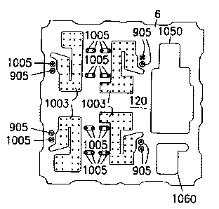
With reference to Fig. l0, subassembly 120 is
manufactured by bonding layers 5, 6 together. Using the
fusion bonding process described above, the top of layer 5 is
bonded to the bottom of layer 6, as shown in Fig. lOc. Then,
136 holes 1003 having diameters of approximately 0.20 mm and
18 holes 1005 having diameters of approximately 0.25 mm are
drilled into subassembly 120 as shown in Figs. l0a and lOb.
Subassembly i20 is sodium etched. Subassembly 120 is cleaned
by rinsing in alcohol for 15 to 30 minutes, then preferably
rinsing in water, preferably deionized, having a temperature
of 21 to 52 degrees C for at least 15 minutes. Subassembly
120 is then vacuum baked for approximately 30 minutes to 2
hours at approximately 90 to 180 degrees C, but preferably
for one hour at 149 degrees C. Subassembly 120 is plated
with copper, preferably first using an electroless method
followed by an electrolytic method, to a thickness of
approximately 13 to 25 microns. Subassembly 120 is
preferably rinsed in water, preferably deionized, for at
least 1 minute. Subassembly 120 is heated to a temperature
of approximately 90 to 125 degrees C for approximately 5 to
30 minutes, but preferably 90 degrees C for 5 minutes, and
then laminated with photoresist. Masks are used and the
22
CA 02320064 2000-08-14
WO 99/41957 PCT/US99/02887
photoresist is developed using the proper exposure settings
to create the patterns shown in Figs. l0a and lOb. The top
side and bottom side of subassembly 120 is copper etched.
Open cutouts 1050, 1060 are formed by milling in two places.
Subassembly 120 is cleaned by rinsing in alcohol for 15 to 30
minutes, then preferably rinsing in water, preferably
deionized, having a temperature of 21 to 52 degrees C for at
least 15 minutes. Subassembly 120 is then vacuum baked for
approximately 30 minutes to 2 hours at approximately 90 to
180 degrees C, but preferably for one hour at 149 degrees C.
d . Layer 7
With reference to Fig. 11, a preferred embodiment
of layer 7 is shown. First, 28 holes 1105 having diameters
of approximately 0.25 mm are drilled into layer 7, as shown
in Figs. ila and llb. Next, layer 7 is sodium etched. Layer
7 is cleaned by rinsing in alcohol for 15 to 30 minutes, then
preferably rinsing in water, preferably deionized, having a
temperature of 21 to 52 degrees C for at least 15 minutes.
Layer 7 is then vacuum baked for approximately 30 minutes to
2 hours at approximately 90 to 180 degrees C, but preferably
for one hour at 149 degrees C. Layer 7 is plated with
copper, preferably first using an electroless method followed
by an electrolytic method, to a thickness of approximately 13
to 25 microns. Layer 7 is preferably rinsed in water,
preferably deionized, for at least 1 minute. Layer 7 is
heated to a temperature of approximately 90 to 125 degrees C
for approximately 5 to 30 minutes, but preferably 90 degrees
C for 5 minutes, and then laminated with photoresist. Masks
are used and the photoresist is developed using the proper
exposure settings to create the patterns shown in Figs. lla
and llb. Both sides of layer 7 are copper etched. Layer 7
is cleaned by rinsing in alcohol for 15 to 30 minutes, then
preferably rinsing in water, preferably deionized, having a
temperature of 21 to 52 degrees C for at least 15 minutes.
Layer 7 is then vacuum baked for approximately 30 minutes to
2 hours at approximately 90 to 180 degrees C, but preferably
for one hour at 149 degrees C.
23
CA 02320064 2000-08-14
WO 99/41957 PCT/US99/02887
e. Subassemb~y 130
With reference to Fig. 12, a preferred embodiment
of layer 8 is shown. First, four holes 1205 having diameters
of approximately 0.25 mm are drilled into layer 8, as shown
in Fig. 12a. Next, layer 8 is sodium etched. Layer 8 is
cleaned by rinsing in alcohol for 15 to 30 minutes, then
preferably rinsing in water, preferably deionized, having a
temperature of 21 to 52 degrees C for at least 15 minutes.
Layer 8 is then vacuum baked for approximately 30 minutes to
2 hours at approximately 90 to 180 degrees C, but preferably
for one hour at 149 degrees C. Layer 8 is plated with
copper, preferably first using an electroless method followed
by an electrolytic method, to a thickness of approximately 13
to 25 microns. Layer 8 is preferably rinsed in water,
preferably deionized, for at least 1 minute. Layer 8 is
heated to a temperature of approximately 90 to 125 degrees C
for approximately 5 to 30 minutes, but preferably 90 degrees
C for 5 minutes, and then laminated with photoresist. A mask
is used and the photoresist is developed using the proper
exposure settings to create the pattern shown in Fig. 12a.
The top side of layer 8 is copper etched. Layer 8 is cleaned
by rinsing in alcohol for I5 to 30 minutes, then preferably
rinsing in water, preferably deionized, having a temperature
of 21 to 52 degrees C for at least 15 minutes. Layer 8 is
then vacuum baked for approximately 30 minutes to 2 hours at
approximately 90 to 180 degrees C, but preferably for one
hour at 149 degrees C.
With reference to Fig. 13, a preferred embodiment
of layer 9 is shown. Layer 9 is spotfaced 1370, 1380 (also
sometimes referred to as "counterbored") as shown in Fig.
13a, to a depth of approximately 130 to 200 microns deep
without breaking through the substrate. Layer 9 is sodium
etched on the spotface (top) side. Layer 9 is cleaned by
rinsing in alcohol for 15 to 30 minutes, then preferably
rinsing in water, preferably deionized, having a temperature
of 21 to 52 degrees C for at least 15 minutes. Layer 9 is
then vacuum baked for approximately 30 minutes to 2 hours at
approximately 90 to 180 degrees C, but preferably for one
hour at 149 degrees C.
24
CA 02320064 2000-08-14
WO 99/41957 PCT/US99102887
With reference to Fig. 14, subassembly 130 is
manufactured by bonding layers 8, 9 together. Using the
fusion bonding process described above, the top of layer 8 is
bonded to the bottom of layer 9, as shown in Fig. 14c. Then,
240 holes 1403 having diameters of approximately 0.20 mm are
drilled into the top of subassembly 130 as shown in Figs. 14a
and 14b. Subassembly 130 is sodium etched. Subassembly 130
is cleaned by rinsing in alcohol for 15 to 30 minutes, then
preferably rinsing in water, preferably deionized, having a
temperature of 21 to 52 degrees C for at least 15 minutes.
Subassembly 130 is then vacuum baked for approximately 30
minutes to 2 hours at approximately 90 to 180 degrees C, but
preferably for one hour at 149 degrees C. Subassembly 130 is
plated with copper, preferably first using an electroless
method followed by an electrolytic method, to a thickness of
approximately 13 to 25 microns. Subassembly 130 is
preferably rinsed in water, preferably deionized, for at
least 1 minute. Subassembly 130 is heated to a temperature
of approximately 90 to 125 degrees C for approximately 5 to
30 minutes, but preferably 90 degrees C for 5 minutes and
then laminated with photoresist. A mask is used and the
photoresist is developed using the proper exposure settings
to create the pattern shown in Fig. 14b. The bottom side of
subassembly 130 is etched. Subassembly 130 is cleaned by
rinsing in alcohol for 15 to 30 minutes, then preferably
rinsing in water, preferably deionized, having a temperature
of 21 to 52 degrees C for at least 15 minutes. Subassembly
130 is then vacuum baked for approximately 30 minutes to 2
hours at approximately 90 to 180 degrees C, but preferably
for one hour at 149 degrees C.
f Subassembly 140
With reference to Fig. 15, subassembly 140 is
manufactured by bonding subassembly 110, layer 4, subassembly
120, layer 7, subassembly 130 together. Using the fusion
bonding process described above, the top of subassembly 110
is bonded to the bottom of layer 4, the top of layer 4 is
bonded to the bottom of subassembly 120, the top of
subassembly 120 is bonded to the bottom of layer 7, and the
top of layer 7 is bonded to the bottom of subassembly 130, as
CA 02320064 2000-08-14
WO 99/41957 PCT/US99/02887
shown in Fig. 15b. Subassembly 130 is heated to a
temperature of approximately 90 to 125 degrees C for
approximately 5 to 30 minutes, but preferably 90 degrees C
for 5 minutes and then laminated with photoresist. A mask is
used and the photoresist is developed using the proper
exposure settings to create the pattern shown in Fig. 15a.
The top side of subassembly 130 is copper etched.
Subassembly I30 is cleaned by rinsing in alcohol for 15 to 30
minutes, then preferably rinsing in water, preferably
deionized, having a temperature of 21 to 52 degrees C for at
least 15 minutes. Open cutouts 1550, 1560, 1570, 1580 are
formed by milling in four places. In a preferred embodiment,
SO Ohm resistors 1581, 1582, 130 Ohm resistors 1585, 1586,
0.68 uF capacitors 1590, 1591, P/N CLC 416 amplifier 1592,
and diode rings 1595, 1596 are installed using solder paste,
such as Sn96Ag04 solder paste .
Subassembly 140 is cleaned by rinsing in alcohol
for 15 minutes, then rinsing in deionized water having a
temperature of 21 degrees C for 15 minutes. Subassembly 140
is then vacuum baked for approximately 45 to 90 minutes at
approximately 90 to 125 degrees C, but preferably for one
hour at 100 degrees C.
a. Layer 10
With reference to Fig. 16, a preferred embodiment
of layer 10 is shown. Layer 10 is spotfaced 1670, 1680, 1690
as shown in Fig. 16a, to a depth of approximately 0.51 mm
deep without breaking through the substrate. Layer 10 is
sodium etched on the spvtface (top) side. Layer 10 is
cleaned by rinsing in alcohol for 15 to 30 minutes, then
preferably rinsing in water, preferably deionized, having a
temperature of 21 to 52 degrees C for at least 15 minutes.
Layer 10 is then vacuum baked for approximately 30 minutes to
2 hours at approximately 90 to 180 degrees C, but preferably
for one hour at 149 degrees C.
h. Bondincx Film 150
With reference to Fig. 17, a preferred embodiment
of bonding film 150 is shown. Open cutouts 1750, 1760, 1770,
1780 are formed by milling in four places, as shown in Fig.
17a. In a preferred embodiment, bonding film 150 is a
26
CA 02320064 2000-08-14
WO 99/41957 PCT/US99102887
thermoset polymer bonding film approximately 38 microns thick
that is cured according to the profile: 300 PSI, with a 30-
minute ramp from room temperature to 180 degrees C, a 65-
minute dwell at 180 degrees C, and a 30-minute ramp to 35
degrees C. Alternatively, bonding film 150 is cured
according to the profile: 300 PSI, with a 15-minute ramp
from room temperature to 105 degrees C, a 10-minute ramp to
180 degrees C, a 65-minute dwell at 180 degrees C, and a 22-
minute ramp to 35 degrees C. In an alternative preferred
embodiment, bonding film 150 is a thermoplastic polymer
bonding film approximately 38 microns thick that is cured
according to the profile of 200 PSI, with a 30-minute ramp
from room temperature to 150 degrees C, a 50-minute dwell at
150 degrees C, and a 30-minute ramp to 35 degrees C. Other
types of bonding film may be used, and the manufacturer's
specifications for bonding are typically followed.
i. Multilayer Structure 200
With reference to Fig. 2, multilayer structure 200
is manufactured by bonding subassembly 140 and layer 100
together, according to the relevant curing profile. The top
of subassembly 140 is bonded, using bonding film 150, to the
bottom of layer 10. Then, eight slots 250 are milled into
multilayer structure 200 as shown in Figs. 2a and 2b.
Multilayer structure 200 is sodium etched. Multilayer
structure 200 is cleaned by rinsing in alcohol for 15 to 30
minutes, then preferably rinsing in water, preferably
deionized, having a temperature of 21 to 52 degrees C for at
least 15 minutes. Multilayer structure 200 is then vacuum
baked for approximately 30 minutes to 2 hours at
approximately 90 to 180 degrees C, but preferably for one
hour at 100 degrees C. Multilayer structure 200 is plated
with copper, preferably first using an electroless method
followed by an electrolytic method, to a thickness of
approximately 13 to 25 microns. Multilayer structure 200 is
preferably rinsed in water, preferably deionized, for at
least 1 minute. Multilayer structure 200 is heated to a
temperature of approximately 90 to 125 degrees C for
approximately 5 to 30 minutes, but preferably 90 degrees C
for 5 minutes, and then laminated with photoresist. A mask
27
CA 02320064 2000-08-14
WO 99/41957 PCT/US99/02887
is used and the photoresist is developed using the proper
exposure settings to create the pattern shown in Fig. 2b.
The bottom side of multilayer structure 200 is copper etched.
Multilayer structure 200 is cleaned by rinsing in alcohol for
15 to 30 minutes, then preferably rinsing in water,
preferably deionized, having a temperature of 21 to 52
degrees C for at least 15 minutes. Multilayer structure 200
is plated with tin or lead, then the tin/lead plating is
heated to the melting point to allow excess plating to reflow
into a solder alloy. Multilayer structure 200 is again
cleaned by rinsing in alcohol for 15 to 30 minutes, then
preferably rinsing in water, preferably deionized, having a
temperature of 21 to 52 degrees C for at least 15 minutes.
Four corner holes 260 and four edge holes 270 having radii of
approximately 1 mm are drilled into multilayer structure 200.
Multilayer structure 200 is de-paneled using a depaneling
method, which may include drilling and milling, diamond saw,
and/or EXCIMER laser. Multilayer structure 200 is again
cleaned by rinsing in alcohol for 15 to 30 minutes, then
preferably rinsing in water, preferably deionized, having a
temperature of 21 to 52 degrees C for at /east 15 minutes.
Multilayer structure 200 is then vacuum baked for
approximately 45 to 90 minutes at approximately 90 to 125
degrees C, but preferably for one hour at 100 degrees C.
X_III. Other Embodiments
It is to be appreciated that one of ordinary skill
in the art may manufacture various circuits based upon the
process disclosed above. For example, different circuits may
be incorporated in a multilayer structure, and the number of
layers used may be varied. One of ordinary skill in the art
may also alter the manufacturing process in an obvious manner
(for example, drilling a different number of holes, using
different masks, adding different devices?.
Additionally, while there have been shown and
described and pointed out fundamental novel features of the
invention as applied to embodiments thereof, it will be
understood that various omissions and substitutions and
changes in the form and details of the invention, as herein
disclosed, may be made by those skilled in the art without
28
CA 02320064 2000-08-14
WO 99/41957 PCT/US99/02887
departing from the spirit of the invention. It is expressly
intended that all combinations of those elements and/or
method steps which perform substantially the same function in
substantially the same way to achieve the same results are
within the scope of the invention. It is the intention,
therefore, to be limited only as indicated by the scope of
the claims appended hereto.
29