Note: Descriptions are shown in the official language in which they were submitted.
CA 02320218 2000-07-28
WO 99/41779 PCT/US99/02625
CRYSTAL ION-SLICING OF SINGLE-CRYSTAL FILMS
SPECIFICATION
TECHNICAL FIELD OF THE INVENTION
This invention is related in general to the field of manufacturing
integrated circuit devices utilizing single-crystal films. More particularly,
the
invention is related to a method for detaching micron-thin single-crystal
metal oxide
films from metal oxide crystal structures for bonding onto growth-incompatible
substrates.
BACKGROUND OF THE INVENTION
Epitaxial liftoff techniques have been used since 1987 for achieving
heterogeneous integration of many III-V and elemental semiconductor integrated
circuits. For example, epitaxial liftoff has been shown to be effective for
integrating
hetero-junction bipolar transistors ("HBT's") and diode lasers on silicon,
gallium
arsenide and other common substrates. Despite this success, however, it has
been
impossible to integrate devices comprised of other important materials, namely
non-
semiconductor materials such as metal oxides, on these common substrates.
A need for integrated circuit devices combining non-semiconductor
materials with conventional substrates has arisen in the field of electro-
optic and
magneto-optic communications. For example, a need has arisen for on-chip
integrated magneto-optical devices, such as optical isolators, for use in
fiber-optic
telecommunications networks. Although commercially available isolators use
bulk
bismuth-substituted yttrium iron garnet ("Bi-YIG"), and other conventional
integrated
isolators require epitaxial growth on gadolinium gallium garnet ("GGG"),
conventional epitaxial growth technologies are subject to the limitations of
high
temperature chemistry, complex stoichiometry and lattice matching.
More importantly, conventional methods are ineffective for growing
single crystal-structures that exhibit good optical and magnetic properties
for
CA 02320218 2000-07-28
WO 99/41779 PCT/US99/02625
2
combination with semiconductor materials. Efforts using sputter growth
technology
for the growth of polycrystalline films, for example, have been unsuccessful
in
yielding single-crystal films with acceptable optical and magnetic properties.
Another need for integrated circuit devices combining non-
semiconductor materials with conventional substrates has arisen in the field
of
microwave communications. For example, the need has arisen for frequency agile
resonators requiring integrated circuit devices. Conventional frequency agile
resonators, made of poly-crystalline materials such as ferroelectric solids,
are
undesirable because of their limited bandwidth and high loss tangents.
Instead, it is
desirable to construct frequency agile resonators and other integrated
microwave
circuits which are made of ferroelectric or magneto-optic single-crystal
films.
Furthermore, conventional epitaxial liftoff techniques as developed for
III-V semiconductors make use of the large differential etch rates between a
buried
sacrificial layer and the epitaxial structure of interest to detach the latter
from its
growth substrate. For example, early epitaxial liftoff techniques were based
on the
high wet etch selectivity of an aluminum arsenide ("AlAs") layer over an
aluminum
gallium arsenide ("A1,,Ga,.,tAs") layer. Subsequent work has demonstrated the
liftoff
of epitaxially grown layers in other III-V materials, all based on selective
etching of
sacrificial epitaxial layers. Conventional bonding techniques for epitaxially
grown
layers have included the use of' adhesives and van der Waals forces on bare
substrates.
Therefore, it is an object of the present invention to provide a method
for detaching micron-thin single-crystal films from crystal structures, such
as
epilayer/substrate or bulk metal oxide crystal structures, for bonding onto
growth-
incompatible substrates.
It is another object of the present invention to provide a method for
detaching micron-thin single-crystal films made of magnetic garnet materials
from
growth-compatible substrates for use in integrated photonics and microwave
circuits.
It is still another object of the present invention to provide a method
for detaching micron-thin single-crystal films made of ferroelectric materials
from
growth-compatible substrates or bulk crystal structures for use in integrated
photonics
and microwave circuits.
CA 02320218 2000-07-28
WO 99/41779 PCT/US99/02625
3
It is yet another object of the present invention to provide a method for
detaching micron-thin single-crystal films from growth-compatible substrates
without
using conventional etching techniques.
Further objects, features and advantages of the invention will become
apparent from the following detailed description taken in conjunction with the
accompanying figures showing illustrative embodiments of the invention.
SUMMARY OF THE INVEN'TION
In accordance with a preferred method of the present invention, a
method is provided for detaching a single-crystal film from a crystal
structure. The
crystal structure, for example, can be an epilayer/substrate crystal structure
or a bulk
crystal structure. The method includes the steps of implanting ions into the
crystal
structure to form a damage layer within the crystal structure at an
implantation depth
below a top surface of the crystal structure, and then chemically etching the
damage
layer to effect detachment of the single-crystal film from the crystal
structure. The
preferred method of the present invention is especially useful for detaching
single-
crystal metal oxide films from metal oxide crystal structures.
In accordance with another preferred method of the present invention,
a method is provided for detaching a single-crystal film from a crystal
structure, the
method including the steps of implanting ions into the crystal structure to
form a
damage layer within the crystal structure at an implantation depth below a top
surface
of the crystal structure, and then exposing the damage layer to a rapid
temperature
increase to effect detachment of the single-crystal film from the growth-
compatible
substrate.
In accordance with yet another preferred method of the present
invention, a method is provided for detaching a single-crystal film from a
crystal
structure, the method including the steps of implanting ions into the crystal
structure
to form a damage layer within the crystal structure at an implantation depth
below the
crystal structure, bonding the crystal structure to a second substrate, and
exposing the
damage layer to a rapid temperature increase to effect detachment of the
single-crystal
film from the crystal structure.
CA 02320218 2000-07-28
WO 99/41779 PCT/US99/02625
4
BRIEF DESCRIPTION OF THE DRAWINGS
For a complete understanding of the present invention and the
advantages thereof, reference is now made to the following description taken
in
conjunction with the accompanying drawings in which like reference numbers
indicate like features and wherein:
FIGS. lA and 1B show an epilayer/substrate crystal structure and bulk
crystal structure, respectively, for providing a single-crystal film according
to the
preferred crystal ion-slicing methods of the present invention;
FIG. 2 shows a preferred method for crystal ion-slicing of single-
crystal films;
FIG. 3 shows an ion implantation step according to the crystal ion-
slicing method of FIG. 2;
FIG. 4 shows an ion implantation step according to the crystal ion-
slicing method of FIG. 2 whereby an epilayer/substrate crystal structure is
used for
forming a YIG or Bi-YIG single-crystal metal oxide film;
FIG. 5 shows an ion implantation step according to the crystal ion-
slicing method of FIG. 2 whereby a bulk crystal structure is used for forming
a
LiNbO3 single-crystal metal oxide film;
FIG. 6 shows an implantation distribution for 3.8 MeV helium ions in
yttrium iron garnet;
FIGS. 7A and 7B are side and top views, respectively, showing an
etching step according to the crystal ion-slicing method of FIG. 2;
FIG. 8 shows a preferred method for crystal ion-slicing whereby
damage to the single-crystal metal oxide film is minimized by encapsulation;
FIG. 9 shows a preferred method for crystal ion-slicing whereby
residual lattice damage and surface roughening is minimized by rapid thermal
annealing;
FIG. 10 shows a preferred method for crystal ion-slicing whereby the
crystal structure is exposed to a rapid temperature increase;
FIG. 11 shows a preferred method for crystal ion-slicing whereby the
CA 02320218 2000-07-28
WO 99/41779 PCT/US99/02625
crystal structure is bonded to a second substrate and is exposed to a rapid
temperature
increase;
FIG. 12 shows a modified crystal structure for use with the method of
FIG. 11 wherein a second substrate is bonded directly onto the top surface of
a single-
5 crystal film; and
FIG. 13 shows a modified crystal structure for use with the method of
FIG. 11 wherein a second substrate is bonded indirectly onto the top surface
of a
single-crystal film.
DETAILED DESCRIPTION OF THE INVENTION
FIGS. 1 A and 1 B show crystal structures for providing single-crystal
films 12 and 19 according to the preferred crystal ion-slicing methods of the
present
invention. Both FIGS. 1 A and I B show portions 15 and 18, respectively, for
forming
the single-crystal films 12 and 19, respectively. Advantageously, the crystal
structures of FIGS. 1 A and 1 B can be metal oxide crystal structures having
metal
oxide portions 15 and 18 for forming single-crystal metal oxide films.
FIG. 1A shows an epilayer/substrate crystal structure l0A having a
substrate 14, an epilayer 15 disposed on a top surface of the substrate 14, an
epilayer/substrate interface 16, and a damage layer 17 disposed in the
substrate 14 a
depth d below the top surface of the epilayer/substrate crystal structure l
OA.
Although the damage layer 17 of FIG. lA is shown to be below the
epilayer/substrate
interface 16, alterriatively the damage layer 17 can be disposed within the
epilayer 15
as required.
The epilayer 15 of FIG. 1 A can be a metal oxide epilayer used for
forming a single-crystal metal oxide film. As such, the epilayer 15 can be a
layer of
magnetic garnet material, preferably yttrium iron garnet ("YIG"), bismuth-
substituted
yttrium iron garnet ("Bi-YIG") or other garnet materials, disposed on the top
surface
of a gadolinium gallium garnet ("GGG") or other growth-compatible substrate.
The
metal oxide epilayer 15 can also be a layer of ferroelectric material, such as
lithium
niobate ("LiNbO3") or strontium titanate ("SrTiO3"), disposed on the top
surface of a
growth compatible substrate. Alternatively, the epilayer/substrate crystal
structure
CA 02320218 2000-07-28
WO 99/41779 PCT/US99/02625
6
10A may include a plurality of the metal oxide epilayers disposed therein.
FIG. 1 B shows a bulk crystal structure l OB for forming a single-crystal
film 19. The bulk crystal structure I OB also includes a damage layer 17
disposed
therein at a depth d below the top surface of the bulk crystal structure l OB.
Advantageously, the bulk crystal structure lOB can be a metal oxide structure
used for
forming a single-crystal metal oxide film. As further shown in FIG. 5, the
bulk crystal
structure I OB of FIG. 1 B is the preferred crystal structure for forming
LiNbO3 single-
crystal films according to the preferred crystal ion-slicing methods of the
present
invention.
FIG. 2 shows a preferred method 20 for crystal ion-slicing a single-
crystal film from a crystal structure. The method includes the steps of
implanting ions
into a crystal structure to form a damage layer within the substrate (Step 22)
and
chemical etching the damage, or "sacrificial," layer from the substrate (Step
24). The
single-crystal film is thereby detached from the substrate for transfer and
bonding
onto a growth-incompatible structure such as silicon or gallium arsenide.
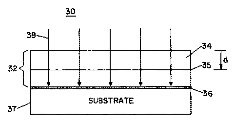
FIG. 3 shows an ion implantation step according to the crystal ion-
slicing method of FIG. 2. Although shown with respect to an epilayer/substrate
crystal structure, the ion implantation step of FIG. 3 is also applicable for
detaching
single-crystal films from bulk crystal structures.
As shown in FIG. 3, elemental ions 38 such as energetic helium or
hydrogen ions, for example, are implanted at a predetermined energy into an
epilayer/substrate crystal structure 30 having a substrate 37, an epilayer 34
disposed
on the substrate 37, and an epilayer/substrate interface 35. The ions can also
be
chemically reactive ions that react with the crystal lattice after
implantation. The ions
are implanted through the epilayer 34 such that a damage layer 36 is formed at
a depth
d below the top surface of the epilayer/substrate crystal structure 30.
Alternatively,
the damage layer 36 can be formed within the epilayer 34.
The ion implantation step introduces lattice defects into the crystal
structure 30 in forming the damage layer 36. The lattice defects are
introduced by the
transfer of energy to the target nuclei, and are formed near the end of the
ionic
trajectories. Depending upon the selected implantation species and ionic
energy, the
CA 02320218 2000-07-28
WO 99/41779 PCT/US99/02625
7
lattice defects and thus the damage layer 36 are introduced into the substrate
37 at a
depth d below the surface of the crystal structure 30.
Referring again to FIG. 3, the thickness of the single-crystal film 32 is
therefore determined by the energy level of the implanted ions 38, which can
be
varied accordingly to yield the desired film thickness. The damage layer, or
"sacrificial" layer, enables the single-crystal film 32 to be "sliced-off' the
top of the
crystal structure 30 for transfer and bonding onto a growth-incompatible
substrate.
FIG. 4 shows a preferred method of FIG. 2 wherein singly-charged 3.8
MeV helium ions 48, for example, are implanted normal to the top surface of an
epilayer/substrate crystal structure 40 to form a damage layer 46 within the
crystal
structure 40. The crystal structure 40 includes a YIG, Bi-YIG or other garnet
epilayer
42, a GGG or other growth-compatible substrate 47, and an epilayer/substrate
interface 45. During implantation, the implantation dose for the singly-
charged 3.8
MeV helium ions is nominally on the order of 5 X 10¹⁶ ions/cm2. The samples
are
mounted on a specially designed, two-inch diameter water-cooled target holder
to
ensure that the temperature of the substrate is below 400 C.
As an added precaution, the current beam during ion implantation is
kept low, gg,,, less than 0.25 A/cm'. This precaution is necessary to avoid
modifying the optical absorptivity atid magnetic anisotropy of the sample
during ion
implantation. The uniformity of the implantation is checked by four Faraday
cups
outside the target holder.
Similarly, as shown in FIG. 5, singly-charged 3.8 MeV helium ions 58
can be implanted normal to the surface of a bulk crystal structure 50 to form
a damage
layer 56 within the crystal structure 40. The bulk crystal structure 50 may be
comprised of a magnetic garnet or ferromagnetic material.
In the preferred method as shown in FIGS. 2 through 5, a light weight
implantation species, preferably helium, is advantageously chosen to yield a
deeply
buried damage layer. In addition, helium is desirable because of the resulting
implantation profile and the distribution of lattice damage in the crystal,
which in turn
is determined by the energy loss per unit trajectory length, or "stopping
power." At
high ionic energies, the "stopping power" is dominated by electronic
scattering and is
CA 02320218 2000-07-28
WO 99/41779 PCT/US99/02625
8
characterized by the Lindhard-Scharff-Schiott ("LSS") theory. The LSS theory
predicts a stopping power proportional to /E, where E is the energy of the
implanted
ion along its trajectory for high ionic energies. At low energies, the
"stopping power"
is inversely proportional to EZ and is primarily characterized by Rutherford
scattering
with the host nuclei.
FIG. 6 shows an implantation distribution profile for helium ions
implanted at 3.8 MeV of energy into a YIG/GGG crystal structure. The
implantation
distribution profile of FIG. 6 is based on simulation results from transport-
of-ions-in-
matter ("TRIM") calculations, which match actual implantation distribution
values for
helium ions implanted at 3.8 MeV of energy into a YIG/GGG crystal structure.
Advantageously, the implantation profile is narrow and concentrated at
approximately
9,um below the surface of the crystal structure. The implantation distribution
profile
for helium ions implanted at 3.8 MeV of energy into a Bi-YIG/GGG crystal
structure
exhibits an almost identical implantation depth.
Referring again to the preferred method 20 of FIG. 2, the ion
implantation step 22 is followed by a chemical etching step for dissolving the
damage,
or "sacrificial," layer from the crystal structure substrate. Once the damage
layer is
dissolved by the chemical etching step, the single-crystal film detaches from
the
substrate and becomes available for transfer and bonding onto a growth-
incompatible
substrate.
FIGS. 7A and 7B are side and top views, respectively, showing an
etching step according to the crystal ion-slicing method of FIG. 2. As shown
in FIG.
7A, a chemical etchant is applied to an epilayer/substrate crystal structure
70 having a
substrate 77, an epilayer 74 disposed on a top surface of the substrate 74,
and a
damage layer 76. After the appropriate exposure period, the chemical etchant
causes
the single-crystal film 72 to become detached from the substrate 74. The
effect of the
chemical etchant is the same whether the damage layer 76 is disposed within
the
substrate 77 or within the epilayer 74 itself. The etch rate, however, may be
vary
depending upon whether the damage layer 76 is disposed within the substrate 77
or
within the epilayer 74.
CA 02320218 2000-07-28
WO 99/41779 PCT/US99/02625
9
Preferably, a commercial 85%-dilution orthophosphoric acid is used
for detaching YIG/Bi-YIG single-crystal films from YIG/GGG or Bi-YIG/GGG
crystal structures. Furthermore, to speed up the chemical etching process, the
orthophosphoric acid is advantageously stirred and maintained at a constant
temperature, preferably 70 C. The temperature of the acid can be further
increased to
achieve faster etching rates.
Nominally, the etchant is applied to the crystal structure 70 for 24 to 48
hours depending upon the size of the single-crystal film to be detached. As
further
shown in FIG. 7A, a deep undercut 78 forms in the substrate 77 after several
hours of
exposure to the chemical etchant. With reference to the implantation steps as
shown
in FIG. 4, for example, the undercut (not shown) is centered at approximately
9 m
below the top surface of the YIG/GGG crystal structure 40 in accordance with
the
implantation distribution profile of FI G. 6. After etching, the substrate 47
is detached
leaving the single-crystal film with an underside that is microscopically
smooth and
suitable for bonding unto a growth-incompatible substrate.
The differential etch rate between sacrificial layer and the rest of the
crystal structure is determined by comparing the etch rate of the undercut 78
to that of
the top surface of the under the same conditions. The latter is determined by
masking
a section of the top surface with silicon dioxide and measuring the etch step
with a
profilometer. The degree of undercut is measured using Nomarski prism
microscopy,
or by cleaving off a section of the single-crystal film overhang. The etch
selectivity,
defined as the ratio of etch rates between sacrificial layer and the top
surface, is found
to be in excess of 103.
For detaching LiNbO3 single-crystal films from bulk crystal structures
such as the one shown in FIG. 5, 5% diluted hydrofluoric acid is preferred for
chemically etching the "sacrificial" layer from the LiNbO3 bulk crystal
structure. The
etching is performed at room temperature for 24 hours or less for detaching a
1 mm2
sample of the LiNbO3 single-crystal film.
As illustrative examples of the present invention, the crystal ion-slicing
method of FIG. 2 has been used to detach magnetic garnet material layers from
a
GGG substrate. In one example, l0 m and 95 m-thick YIG epilayers were grown by
CA 02320218 2000-07-28
WO 99/41779 PCT/US99/02625
liquid phase epitaxy on a GGG substrate containing small amounts of lanthanum
to
improve lattice matching to the GGG substrate. In another example, 3,um-thick
Bi-
YIG thin-films also grown on a GGG substrate. In both cases, the method of
FIG. 2
was used to detach high quality single-crystal films approximately 9 to 10 ,um-
thick
5 from the original substrates. The single-crystal films were then van der
Waals bonded
to growth-incompatible substrates such as silicon and gallium arsenide
substrates.
Faraday contrast examination of the magnetic domains of the single-crystal
films
indicated no change in the domain structure and coercivity of the garnet
materials as a
result of the crystal ion-slicing process.
10 Referring again to the preferred method of FIG. 2, the chemical etching
step may however result in residual lattice damage, surface roughening or
corner
fracturing of the top surface of the single-crystal film. For example, using a
surface
profilometer, six hours of exposure under typical etching conditions has been
shown
to yield an average roughness of 20 nm in the YIG/GGG example of FIG. 4. In
addition, corner fracturing may occur during the chemical etching step as
shown by
the broken lines of FIG. 7B. Consequently, additional protective measures are
required to minimize damage to the single-crystal film and to ensure the
production of
high quality thin-films.
FIG. 8 therefore shows a preferred method 80 for crystal ion-slicing a
single-crystal film from a crystal structure whereby residual lattice damage
and
surface roughening is minimized by encapsulation. The method 80 includes the
steps
of implanting ions into a crystal structure to form a damage layer within the
substrate
(Step 82), encapsulating the top surface of the single-crystal film (Step 84),
and
chemically etching the damage layer from the substrate (Step 86). According to
a
preferred aspect of the present invention, the corners of the single-crystal
film 72 of
FIG. 7 are encapsulated with molten wax or an Apiezon W mixture to prevent
fracturing of the single-crystal film due to the residual lattice damage and
surface
roughening caused by the subsequent chemical etching step.
FIG. 9 shows a preferred method for crystal ion-slicing a single-crystal
film from a crystal structure whereby residual lattice damage and surface
roughening
is minimized by rapid thermal annealing. The method 90 includes the steps of
CA 02320218 2000-07-28
WO 99/41779 PCTIUS99/02625
11
implanting ions into a crystal structure to form a damage layer within the
substrate
(Step 92), rapid thermal annealing (Step 94) and chemical etching of the
damage layer
from the substrate (Step 96).
As shown in FIG. 9, the rapid thermal annealing step (Step 94) is
performed after the ion implantation step (Step 90) but before chemical
etching step
(Step 96). The rapid thermal annealing serves to repair the residual damage
without
compromising the efficiency of the subsequent wet etching of the buried layer.
Preferably, a 40 second anneal at 700 C in forming gas comprised of 5%
hydrogen
and 95% nitrogen results in a smooth surface and thus high-quality single-
crystal
films. By contrast, a rapid temperature annealing step performed at
temperatures
above 80`0 C is undesirable since it significantly impairs the etch rate of
the buried
layer by annealing out the damage in the "sacrificial" layer. Consequently,
the
method of FIG.9 including the rapid temperature annealing step (Step 94)
performed
at approximately 800 C will reduce the etch rate associated with the
subsequent
chemical etching step (Step 96) as compared to a method not including the
rapid
temperature annealing step (Step 94).
Referring again to the preferred method of FIG. 2, the duration of the
chemical etching step 24 is nominally 24 to 48 hours depending upon the size
of
single-crystal film to be detached. For example, to fully detach a square-
millimeter
area section of film from a substrate, the crystal structure must be exposed
to the
etchant for approximately 24 to 48 hours.
Therefore, as a faster alternative to the method of FIG. 2, FIG. 10
shows another preferred method 100 for crystal ion-slicing a single-crystal
film, from
either an epilayer/substrate or bulk crystal structure, whereby the crystal
structure is
exposed to a rapid temperature increase to effect detachment of the single-
crystal film
from the growth-compatible substrate. The method 100 includes the steps of
implanting ions into a crystal structure below the epilayer/substrate
interface to form a
damage layer within the growth-compatible substrate (Step 100), and exposing
the
crystal structure to a rapid temperature increase so as to effect the
detachment or
"snap-ofP' of the single-crystal film from the growth-compatible substrate
(Step 102).
The exposure step 102 of FIG. 10 includes raising the temperature of the
crystal
CA 02320218 2000-07-28
WO 99/41779 PCT/US99/02625
12
structure from room temperature to approximately 750 to 800 C within 60
seconds.
Detachment of the single-crystal film is thereby achieved by maintaining the
temperature of the crystal structure at approximately 750 to 800 C for
approximately
30 seconds.
As an additional step, the damage layer may be chemically treated
during or before ion implantation with a chemically enhancing gas, such as
chlorine
gas, or liquid to enhance detachment of the single-crystal film. Chemical
treatment of
the damage layer may also be performed so as to minimize the degree of the
rapid
temperature increase required to effect detachment of the single-crystal film
from the
crystal structure.
FIG. 11 shows a preferred method 110 for crystal ion-slicing a single-
crystal film from a crystal structure whereby the crystal structure is bonded,
directly
or indirectly, to a second substrate and exposed to a rapid temperature
increase to
detach the single-crystal film from the growth-compatible substrate. The
method can
be used with the epilayer/substrate crystal structure of FIG. 1 A and as
further shown
in FIGS. 12 and 13, or the bulk crystal structure of FIG. 1B.
Referring again to FIG. 11, the method 110 includes the steps of
implanting ions into a crystal structure to form a damage layer within the
crystal
structure (Step 110), bonding the top surface of the single-crystal film,
either directly
or indirectly, to a second substrate (Step 112), and exposing the crystal
structure to a
rapid temperature increase so as to effect the detachment or "snap-off' of a
single-
crystal film from the crystal structure (Step 114). As with the method of FIG.
10, the
exposure step (Step 114) includes raising the temperature of the crystal
structure from
room temperature to approximately 750 to 800 C within 60 seconds. Detachment
of
the single-crystal film is thereby achieved by maintaining the temperature of
the
crystal structure at approximately 750 to 800 C for at approximately 30
seconds.
The second substrate according to the bonding step (Step 112) is
advantageously bonded directly onto the top surface of the crystal structure,
preferably by the technique of direct wafer bonding as described by Yokoi et
al. in
"Improved heat treatment for wafer direct bonding between semiconductors and
magnetic garnets, " Japan Journal of Applied Physics, vo136, p. 2784 (1997).
The
CA 02320218 2000-07-28
WO 99/41779 PCT/US99/02625
13
second substrate can be a semiconductor such as silicon or GaAs. This method
is
advantageous in that the single-crystal film layer remains bonded to the
second
substrate after the single-crystal film is detached from the crystal
structure.
Alternatively, the method of FIG. 11 may include the step of applying
a low-temperature bonding layer between the top surface of the crystal
structure and
the second substrate. The function of the low-temperature bonding layer is to
avoid
annealing out the damage or sacrificial layer during the detachment process.
This
technique is the same regardless of whether an epilayer/substrate or bulk
crystal
structure is used.
FIG. 12 shows a modified crystal structure 120 for use in the preferred
method of FIG. 11. By way of example and not limitation, the modified crystal
structure 120 is similar to the epilayer/substrate crystal structure shown in
FIG. IA.
The modified crystal structure 120 includes a first, growth-compatible
substrate 127,
the second substrate 128, an epilayer 124 disposed between the first and
second
substrates 127 and 128, and a damage layer 126 disposed in the first substrate
127 a
depth d from the interface 125 between the epilayer 124 and the second
substrate 128.
The first and second substrates 127 and 128 are preferably bonded together by
direct
wafer bonding. The epilayer 124 is preferably a layer of magnetic garnet or
ferroelectric material mounted between the first substrate 127 such as GGG or
other
growth-compatible substrate.
FIG. 13 shows another modified crystal structure 130 for use in the
preferred method of FIG. 11 wherein the second substrate 128 is indirectly
bonded to
the single-crystal film 124. As shown in FIG. 13, the modified crystal
structure 130,
by way of example and not limitation, includes a first, growth-compatible
substrate
127, a second substrate 128, an epilayer 124 disposed between on the first
substrate
127, a bonding layer 132 disposed between the epilayer 124 and the second
substrate
128, and a damage layer 126 disposed in the first substrate 127 a depth d from
the
interface 125 between the epilayer 124 and the second substrate 128.
As shown in FIG. 13, the epilayer 124 is preferably a layer of magnetic
gatnet or ferroelectric material mounted between the first substrate 127,
which is
preferably a GGG or other growth-compatible substrate. The bonding layer 132
is
CA 02320218 2000-07-28
WO 99/41779 PCT/US99/02625
14
preferably a low temperature melting material, such as low temperature melting
glass,
which has a melting point less than the 750 to 800 C temperature plateau of
Steps
104 and 116 of FIGS. 10 and 11, respectively.
Although the present invention has been described in connection with
particular embodiments thereof, it is to be understood that such embodiments
are
susceptible of modification and variation without departing from the inventive
concept disclosed. All such modifications and variations, therefore, are
intended to be
included within the spirit and scope of the appended claims.