Note: Descriptions are shown in the official language in which they were submitted.
CA 02320348 2000-08-04
s
s
1
Heatable mirror aad process for producing a heat-
conducting layer as well as its use
The invention relates to a heatable mirror having a
specially designed heat-conducting layer made from
conductive particles, a process for applying heat-
conducting layers to substrates and the use of this
process for producing heatable mirrors.
Heatable mirrors having a heat-conducting layer made from
conductive material are known. Hence a heatable mirror is
described in United States 3 686 43~ in which a heat-
conducting layer has been applied to a glass substrate
under vacuum or by sputtering. This United States patent
proposes the use of a nickel-chromium alloy as the heat-
conducting layer.
The disadvantage of this mirror is that firstly, the
technologies for applying the heat-conducting layer are
very complex. As described in the United States patent,
application of the nickel-chromium alloy should be
carried out either under vacuum or using a sputtering
process. Both process steps are too complex and too
expensive for mass production. Furthermore, it has been
shown that a mirror of this type obviously also does not
have adequate heat capacity due to the only very thin
layers. This leads to the time span for keeping a mirror
free of condensation being too long. Also it is not
possible using mirrors of this type to heat certain areas
specifically more strongly than others, which is required
is many cases because of the construction of the mirror.
The object of the present invention is therefore to
propose a heatable mirror, the heat-conducting layer of
which permits high heat capacity and any design of layout
for the heat-conducting layer. The object of the
' CA 02320348 2000-08-04
2
invention is also to provide a cost-effective and simple
process for mass production, by means of which a heat-
conducting layer may be applied to a substrate.
The object is achieved with regard to the heatable mirror
by the features of patent claim 1 and with regard to the
process by the features of patent claim 17. The sub-
claims show advantageous further developments of the
solution according to the invention.
It is thus proposed according to the invention that the
heat-conducting layer is formed by conductive particles
at least partially embedded in the surface of the
substrate and/or the reflective layer. It is thus
essential for the heatable mirror of the invention that
the particles have an average diameter of 3 to 100 ~.m.
Figures 4 to 6 show scanning electron-microscope images
in 30, 100 and 1,000 times magnification, from which
particle formation can be seen. Accordingly, the heat-
conducting layer has a "rough surface". Figure 6 in
particular shows that the particles have obviously only
been changed insignificantly by the application process.
Figures 4 to 6 also show that the particles have
partially penetrated into the surface of the substrate,
here a mirror. Adhesion of the particles to the substrate
is thus essentially produced by the penetration of
particles into the surface of the substrate. Of course
partial sintering of the particles with one another and
with the surface also takes place. It is important for
the heatable mirror having the heat-conducting layer as
described above, that a certain roughness, that is an
average particle diameter of 3 to 100 ~m is maintained,
and that a thus cohering conductive layer is produced.
The heat-conducting layer of the mirror of the invention
thus differs from those which are known hitherto from the
state of the art, which have been applied conventionally
via sputtering processes or evaporation methods. In all
' CA 02320348 2000-08-04
3
these cases a very finely divided homogeneous conducting
layer is thus produced which has the disadvantages of the
state of the art outlined in the introduction.
The particles themselves are preferably selected from the
metals A1, Zn, Sn, Cu, Ni and/or alloys thereof. It is
most particularly preferred for the heatable mirror of
the invention if the particles consist of aluminium
and/or an aluminium alloy having at least 96 ~ aluminium.
A further preferred embodiment of the mirror of the
invention is characterised in that the substrate for the
heatable mirror is glass. The material pairing glass and
aluminium and/or aluminium alloy in particular as
particles has proved to be particularly superior in its
properties with regard to the mechanical adhesion and
electrical heat capacity.
For the mirror of the invention, the heat-conducting
layer may be designed to be both over the entire surface
or strip-like. For the embodiment in which a strip-like
heat-conducting layer is present, it is thus important
that the regions between the heat-conducting strips
consist of an insulating separating layer. This
insulating separating layer is preferably a thin film
having a width of 0.2 mm to 1 mm. The minimum width is
important because otherwise bridging may occur during
spraying. The separating layer is produced from a
formulation containing resins and solvents. Preferred
resins are thus shellac, gum arabic or colophony. The
insulating separating layer may thus also contain further
additives, as known per se from the state of the art.
This separating layer is applied in the required form by
spreading-on, spraying or brushing.
It has also proved to be advantageous if the layer
thickness of the heat-conducting layer lies in the range
f rom 10 ~.m to 100 ~cm, preferably in the range f rom 4 0 to
' CA 02320348 2000-08-04
.
4
60 wm. A particular advantage of the heatable mirror of
the invention is that the layer thickness of the heat-
conducting layer may be selected to be different, so that
increased heat capacity is then obtained at particularly
critical points in the mirror area, so that condensation
is also prevented there. For the case that strip-like
heat-conducting layers are used, the strip widths of the
heat-conducting layer are 2 to 20 mm. Also the strip
width of the heat-conducting layer may be selected to
correspond to the width so that a wider strip width is
selected at particularly critical points at which
dehumidification of the mirror is only possible with
difficulty. Of course the invention also includes all
embodiments in which both the layer thickness of the
layer and also the strip width is varied.
The heat-conducting layer of the heatable mirror of the
invention also shows considerable improvement compared to
the state of the art apart from the advantages described
above. It has also been shown to the expert in a manner
which could not be foreseen, namely that the heat-
conducting layer as defined in patent claim 1 may be
provided with a polymer coating which serves as chip
protection, for thermal and electrical insulation as well
as also as adhesive for fixing the mirror frame.
It was hitherto namely conventional in the state of the
art to apply chip protection which was present in the
form of adhesive films or foils and which had to be
produced in a separate working step and then adhered to
the mirror. In the mirror of the invention it is now
possible to apply a polymer coating very simply, for
example by spraying, particularly because of the surface
formed by the particles. It has thus proved to be
particularly advantageous if as the polymer coating such
a one is selected which consists of a self-curing silane-
modified polymer. This now produces the advantage that
" CA 02320348 2000-08-04
,
the mirror is coated over the entire surface with the
polymer on the side on which the heat-conducting layer is
applied in a single working step, and that simple curing
in air then takes place. Silane-modified alkyd resin
systems are preferably used as polymers of this type.
They are characterised particularly in that they are
single-component systems and cross-link in air moisture
to give a flexible product. A further advantage of such a
coating is that this coating acts as a steam barrier and
is W stable and functions as a sealing material with
very good workability.
In the heatable mirror of the invention provision is
made, as already known from the state of the art, in that
contact points are present for contacting with a voltage
source. These contact points are thus preferably designed
so that they are connected to the heat-conducting layer
via an additional metal layer. This additional metal
layer is preferably selected from the metals Zn and/or
Sn. This additional metal layer thus has a thickness of
50 to 100 ~,m.
The layers known from the state of the art may be used as
the reflective layer for the mirror. Examples of these
are dichroic layers or chromium or silver layers.
The invention also relates to a process for producing a
heat-conducting layer made from electrically conductive
particles on a substrate. The process is characterised
according to the invention in that the electrically
conductive material is supplied to a heat-producing
device in wire form and thus exposed to a temperature of
> 5,000°K. The conductive particles thus produced are
conveyed in air onto the substrate surface. It is thus
important in the process of the invention that this
application process is carried out in ambient atmosphere,
' CA 02320348 2000-08-04
6
that is in room air. Hence this process is simple and
cost-effective to construct.
It is preferable in the process of the invention if the
heat is produced by means of electric arc. The distance
between the device and the substrate is thus preferably 5
to 50 cm, particularly preferably 12 to 25 cm. It should
be emphasised in particular for the process of the
invention that the particles may be transported using
compressed air. As a result of this simple measure it is
now possible to also influence the process by varying the
pressure. The compressed air may be varied in the range
from 2.8 to 7.5 atmospheres.
The process of the invention thus permits the layer
thickness of the particles applied to be adjusted by
varying the distance of the substrate from the heat-
producing device and/or by varying the speed of the
particles as well as by the wire feed and the level of
the electric arc current.
The process of the invention offers wide-ranging
advantages. According to the invention a separating layer
should be produced on the substrate as a first process
step for the strip-like embodiment. This separating layer
is thus designed as regards its structure so that during
application the heat-conducting layer obtains the
required strip shape, for example meandering or helical.
Surprisingly, it has been shown that such an insulating
separating layer may be produced very simply by applying
a formulation containing a resin and a solvent. It has
been shown that if such an insulating layer is applied to
the substrate surface by an application process which is
conventional per se, the particles supplied to the
substrate by the evaporation method at the points at
which the separating layer adheres to the substrate,
' CA 02320348 2000-08-04
7
penetration of the particles into the substrate surface
is prevented. The particles landing thus fall off from
these regions on which the separating layer is applied
and only adhere, that is they penetrate into the surface
of the substrate, at the points at which there is no
separating layer. Figures 4 to 6 now show, by way of
example on a glass substrate, an applied aluminium alloy
in which a separating layer is also present. Figures 4 to
6 illustrate that at the points at which the separating
layer has been applied by the subsequent application
process, adhesion of the particles has not taken place.
In the example of Figures 4 to 6, a marker pen having a
resin formulation and dyestuffs was used as the
separating layer.
This opens wide-ranging possibilities with regard to the
layout of the heat-conducting layer to be applied. Using
the process of the invention it is thus not only possible
to vary the thickness and the strip width, but also the
layout of the heat-conducting layer to be applied may be
controlled specifically by very simple application of the
separating layer on the substrate.
One crucial advantage of the process of the invention is
that a polymer coating may be applied over the entire
surface of the heat-conducting layer which then serves as
chip protection, for thermal and electrical insulation as
well as adhesive for fixing the mirror frame. It is
obviously possible that a polymer coating may be applied
by means of a simple process, for example by rolling,
spreading or another conventional application process,
particularly due to the rough surface produced by the
process of the invention having the particle formation
described above. A further advantage is that this polymer
coating has excellent adhesion to the base, that is to
the conducting layer and/or to the separating layer. A
silane-modified polymer, in particular a silane-modified
' CA 02320348 2000-08-04
8
alkyd resin, is preferably used as the polymer coating.
The advantage of this system consists in that it is self-
curing in air. As a result of this measure very simple
and cost-saving application of chip protection is
possible which at the same time serves as insulation and
optionally as adhesive for the mirror frame.
With regard to the selection of material for the
particles to be applied and for the substrates, reference
is made to the above statements for the heatable mirror.
Accordingly, it is particularly preferable if a material
pairing glass and aluminium and/or aluminium alloy is
used for the particles. For the insulating separating
layer it has thus been proved to be advantageous if a
marker pen known per se from the state of the art, for
example Eddingmarker°, is used here.
As a result of the excellent control possibilities of the
process with regard to layer thickness, strip width and
the layout, the process of the invention described in
more detail above is particularly suitable for producing
heat-conducting layers for heatable mirrors in the motor
vehicle industry, as described in claims 1 to 16.
The invention is described in more detail below using
Figures 1 to 7.
Figure 1 shows a mirror having a heat-conducting layer
designed according to the invention;
Figure 2 shows the mirror, sectioned along the lines II -
II in Figure 1;
Figure 3 shows a partial area of the mirror of the -
invention having a moisture sensor and energy supply and
control device shown schematically;
" CA 02320348 2000-08-04
9
Figure 4 shows an electron-microscope image in 30 times
magnification of a heat-conducting layer of the
invention;
Figure 5 shows the same heat-conducting layer in 100
times magnification;
Figure 6 shows the heat-conducting layer in 1,000 times
magnification.
By way of introduction it should be remembered that the
same parts are provided with the same reference symbols
or the same component designations in the different
embodiments described, wherein the disclosures present in
the whole description may be transferred analogously to
the same parts with the same reference symbols or the
same component designations. Also the positional details,
such as for example top, bottom, side etc., selected in
the description, relate to the figure actually being
described and shown, and should be transferred
analogously to the new position for a change of position.
Furthermore, individual features or feature combinations
from the different exemplary embodiments shown and
described in themselves may also be independent,
inventive solutions or solutions according to the
invention.
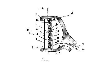
In Figures 1 to 3 described together, a heatable mirror 1
having a heating element 2 in a housing 3 is shown for an
external mirror 4, for example for motor vehicles. It
consists of a substrate 5 made from an inorganic
material, for example glass, ceramic, having low thermal
conductivity, preferably with ground and coated surfaces
6, 7. The substrate 5 having a reflective layer 9, for
example a chromium layer, is coated for example on the
surface 7 opposite a viewing direction according to -
arrow 8.
' CA 02320348 2000-08-04
The heating element 2 having a layer applied at least to
one surface 6, 7 of the substrate 5 and/or reflective
layer 9 and made from electrically conductive material
providing a resistance to the current flow, essentially
forms a conducting strip 10, wherein the electrically
conductive material is arranged on the surface 6, 7 like
a strip or over the entire surface. The strip-like path
of the conducting strip 10 is helical or meandering, the
surface 7 is preferably designed to cover a large area,
wherein an interruption-free path for the conducting
strip 10 is provided by an end position situated
approximately in the centre of a longitudinal end edge 11
up to a further end position arranged immediately
adjacent to it. However, it is also possible to design
the conducting strip 10 as a full-surface heating layer.
Contact elements 12, 13 are arranged in the end positions
of the conducting strip 10.
Conducting strip regions 14, 15 running immediately
adjacent one another are insulated electrically from one
another by means of a separating layer 17 forming a gap
16 between the conducting strip regions 14, 15 and which
is arranged on the surface 6, 7 of the substrate 5. The
contact elements 12, 13, of which leads 18, 19 are passed
through housing 3 for electrical supply of conducting
strip 10, are connected to be electrically conductive by
direct soldering with the material of the conducting
strip 10 and consist of a zinc and/or tin layer applied
to the conducting strip 10.
The heating element 2 is provided with a covering layer
21 of electrically non-conductive material on a rear
surface 20 facing away from the substrate 5, so that the
conducting strip 10 is arranged between substrate 5 and
the covering layer 21. The covering layer 21 is thus
preferably formed by a self-curing polymer coating, for
example of silane-modified polymer. The mirror 1 is
' CA 02320348 2000-08-04
11
adhered into the mirror frame 22 using the covering layer
21 and is held in housing 3 by the support 23.
The conducting strip 10 running between separating layer
17 is formed by particles 24 made from electrically
conductive material applied to adhere to the surface 7 by
means of electric-arc processes. Particles 24 of Al,, Zn,
Sn, Cu, Ni and/or alloys thereof are preferably used,
wherein the conducting strip 10 for converting current
energy to heat energy for supply from a low-voltage mains
supply, has a preset resistance value of about 2 ~ to 20
n, preferably 8 n. The temperature of the conducting
strip 10 exposed to current is thus a maximum 100°C.
However, the electrically conductive material or the
conducting strip 10 may also be designed to be
transparent, for example as a hard glass coating, which
is preferably arranged on a front side of the substrate 5
facing the viewing direction - arrow 8, in particular on
a front side of the heatable mirror 1 facing a viewing
direction - arrow 8.
To achieve different temperature zones distributed over
the substrate 5, the heating element 2 is provided with a
continuously changing layer thickness 25, with which, for
a preset strip width 26 of the lead cross-section and
hence the lead resistance opposing the current flow, it
is possible to adapt to the requirements for heat
capacity in different zones of the mirror 1.
However, even heat voltages between adjacent regions in
the substrate 5 are effectively prevented by the design
of the heating element 2 of the invention having
continuously changing layer thickness 25 of the
conducting strip 10, as a result of which it is possible
to use very thin-walled substrates 5 without voltage
breaks occurring, and reduction of energy use, as well as
CA 02320348 2000-08-04
12
shorter response times, is subsequently achieved due to
the low mass to be heated.
Of course the mirror 1 of the invention may be used not
only for the external mirror 4 shown, but also for all
external mirrors conventional today, such as for example
for electrically adjustable external mirrors.
It is also possible to combine the mirror 1 fitted with
the heating element 2 with one or more sensors, for
example heat sensors 28 or moisture sensors 29, which may
be arranged on the surface 7 or on a surface 6 opposite
the conducting strip 10 of a surface element preferably
formed by the substrate 5 and optionally the reflective
layer 9.
One possible design of the moisture sensor 29 consists,
for example in the design of a resistive measuring area,
as shown in Figure 3. The sensor may be formed by a part
region of the electrically conductive material arranged
to be insulated from the conducting strip 10, in
particular from the heating layer. However, electrically
conductive contact surfaces 30, 31, for example due to a
chromium coating, may also be applied to the surface 6 or
7 in an edge region 27 of the mirror 1 or in the region
of a longitudinal end edge 11 of the substrate 5, and
which are insulated from one another, for example by the
separating layer 17. An electrical voltage is applied to
the contact surfaces 30, 31 via leads 32, 33. If moisture
forms on the surface 6, as occurs during condensation or
freezing, there is current flow due to bridging of the
separating layer 17 and the signal derived therefrom may
be used as a switch signal to activate the heating
element 2 in a corresponding supply and/or control device
34.