Note: Descriptions are shown in the official language in which they were submitted.
CA 02321007 2000-08-17
WO 99/42216 PCT/US99/03575
Bead Transporter Chucks Using Repulsive Field Guidance
The present invention is directed to devices for electrostatically picking up
and
dispensing beads in a spatially resolved manner. Specifically, this disclosure
describes improved
electrode configurations and operation techniques for electrostatic bead
transporter chucks that
pick up, manipulate, transport, and then discharge or place beads or objects
for use in creating
pharmaceutical or chemical compositions, or in performing assays or chemical
analysis.
Bead transporter chucks act as clamps to hold or retain beads. Bead
transporter chucks
provide superior performance for manipulating synthetic beads having typical
diameters of 100-
300 microns in chemical synthesis, such as combinatorial chemistry for solid
phase synthesis, or
in an assay using PCR (polymerase chain reaction), or other processes. 1n
combinatorial
chemistry, a mufti-well array such as a microtiter plate allows screening or
synthesis of many
compounds simultaneously.
For example, bead transporter chucks allow deposition of beads on an array in
a manner
that is faster and more reliable than by the use of micropipettes, which can
be inefficient,
tedious, and time consuming. Another application for bead transporter chucks
is synthesis of
pharmaceutical compositions, especially when used to combine compounds to form
compositions to be packaged into administration forms for humans or animals.
Beads containing one or more active ingredients may be deposited onto well
known
carriers or substrates to make pharmaceutical dosage forms. Such beads may
take the form, for
example, of [ 1 ] a powder, such as dry micronized fonws made by air jet
milling processes, where
overall particle dimensions can be, for example, in the 1 to 10 micron range
useful for dry
powder respiratory administration of medicaments, with 4 - 8 microns
preferred; [2]
microspheres; [3] extremely small structures, including fullerenes, and
chelates; or [4] liposomes
and fatty droplets formed from lipids or cell membranes.
The use of bead transporter chucks provides a customized and precise method
for
formulating drug compositions. The transporter can be used to merge adjacent
substrates
carrying active ingredient to form multidosage packs, in which dosage can
decrease or increase
from one individual unit to the next, as in hormone-based (e.g., birth
control) drugs or antibiotic
remedies. Using an electrostatic bead transporter chuck, dosages may be easily
established or
determined by the number and/or type of beads dispensed onto each
pharmaceutical carrier.
Using bead transporter chucks to place active ingredients into pharmaceutical
compositions can
give high repeatability and is also advantageous when the active ingredients
are not compatible,
_1_
CA 02321007 2000-08-17
WO 99/42216 PCTNS99I03575
such as when the active ingredient is poorly soluble with the carrier, or
where a formulation
carrier negatively affects the bioavailability of the active ingredient.
Although emphasis is placed in this disclosure on electrostatic bead
transporter chucks
using electric fields for bead retention and/or release, the teachings given
here may be applied to
chucks using other phenomena, such as the use of compressed gas or vacuum, or
electrically/chemically switchable adhesives, in controlling beads.
Electrostatic holding
mechanisms, however, are far more benign to delicate bead structures than
traditional
mechanical techniques, particularly when manipulating biologically active
compounds where
crushing, contamination, or oxidative damage must be minimized or eliminated.
The present invention may also be used in conjunction with acoustic bead
dispensers,
where acoustic energy, provided by a speaker or piezoelectric device, is used
to great advantage
in bead control, that is, propelling and/or tribocharging beads prior to, and
especially during,
electrostatic manipulation. Tribocharging beads, as known in the art, and
described below, is
more efficient and less damaging to the beads than corona or plasma charging,
which typically
requires high applied voltages of around 5 kV. Often, the sonically vibrating
membrane used in
such an acoustic bead dispenser may itself be used to tribocharge the
particles, eliminating the
need to charge the beads prior to their entry into the acoustic dispenser. The
use of acoustic
dispensers allows polarity discrimination of beads, where wrongly charged
beads are
discouraged from being retained by the bead transporter chuck.
In the course of bead manipulation and control, particularly when using
electric fields
and polarization to guide beads, certain problems arise and certain
requirements have become
apparent.
First, it is desirable to have one, and only one bead to be attracted,
transported, and
discharged for each bead transporter chuck, or for each well, pixel, or
individual spatial element
of the bead transporter chuck. This is especially true for certain
embodiments, where each pixel
may be considered a tiny bead transporter chuck that is selectively and
independently controlled,
such as planar chucks having individually addressable x and y coordinates.
This includes
individually addressable pixels for different (multiple) bead types.
Second, beads manipulated by the bead transporter chuck must be easily and
controllably releasable, with wrongly charged beads (objects or beads having a
charge of the
opposite polarity desired) not occupying bead retaining or collecting zones on
the bead
transporter chuck.
-2-
CA 02321007 2000-08-17
WO 99/42216 PCT/US99I03575
Third, the bead transporter chuck should function well for a wide range of
bead
diameters, including beads with general dimensions of 100 microns and up, and
especially
porous or hollow beads that have high charge/mass ratios.
Fourth, bead transporter chuck components should be durable, re-usable, and
preferably
have good ease-of use, including having selectively or wholly transparent
elements for easy
movement and alignment of the chuck with intended targets or carriers.
Methods for use of bead transporter chucks and acoustic bead dispensers are
set forth in
Sun, "Chucks and Methods for Positioning Multiple Objects on a Substrate," US
Application
No. 08/630,012, filed 09 April 1996; Sun et al., "Electrostatic Chucks," US
Application No.
08/661,210, filed 10 June 1996; Pletcher et al., "Method and Apparatus for
Electrostaticaiiy
Depositing a Medicament Powder Upon Predefined Regions of a Substrate," US
Application
No. 08/659,501, filed 06 June 1996; and Sun et al., "Acoustic Dispenser," US
Application No.
08/661,211, filed 10 June 1996.
Bead transporter chuck designs that use simple attraction electrodes to pick
up and
discharge beads can, under cer<ain conditions, encounter serious problems with
bead density and
control. One problem encountered is that many more beads than desired are
attracted to
intended bead collection zones. During synthesis or analysis, instead of
retaining one and only
one bead per bead collection zone, multiple beads or even whole clumps of
beads are attracted to
bead collection zones when using typical or desired attracting voltages needed
for e~cient
manipulation of the beads. Alternatively, in seeking to avoid this bead
clumping by reducing the
applied (attraction) voltage, the attraction field is then not sufficient to
cause beads to deposit in
the required manner, i.e., one bead per hole, without either having beads
attracted to unintended
or wrong locations on the bead transporter chuck, or having wrongly charged
beads attracted to
the bead transporter chuck.
It is important to keep in mind that particle charging -- whether by
triboelectric and
contact transfer, corona charging, or thermionic and field emission charging --
occurs essentially
at the particle surfaces. These surface effects are well known, and are aided
by electric
polarization, that is, induced surface charge in response to an applied
electric field. Polarization
is ubiquitous in nature. A charged rod, for example, will attract uncharged
bits of paper, etc.
However, the problem in bead pickup and dispensing is one of balancing
electrical
fields, and making non-uniform fields that will guide beads singly to intended
bead collection
zones. In attracting and manipulating beads, image charges, and electric
polarization play a role.
-3-
CA 02321007 2000-08-17
WO 99142216 PCT/US99/03575
In particular, it is well known that dielectrics, such as polymer beads, that
are placed in a
uniform electric field will not experience a net force. In an essentially
uniform field, such as
between two large charged plates, the induced surface charge or charge
shifting that results from
electric polarization does not yield any significant net force on a neutral or
uncharged object. To
include the action of neutral beads, and for maximum bead guidance and
attraction, it is desired
to have non-uniform fields whose fields lines converge or diverge. ff one uses
uniform electric
fields, the applied voltages required to attract and retain beads causes too
many beads to be
retained at bead collection zones.
To illustrate this, Dupont~ Kapton° polyimide film with a copper
exterior metallization
may be used in a closed container to attract beads using a simple uniform
electric field. A
simple bead transporter chuck comprising a planar electrode, copper on Kapton
, forms the top
of the container. The copper/Kapton° planar electrode of the chuck may
have bead holes or
apertures to act as bead collection zones into which the attracted beads may
nestle. A voltage of
3000 volts is applied between [ 1 ] the planar copper/Kapton°
electrode; and [2] a conductive
base plate or mesh at the bottom of the container. After precharging 105 mg of
280 micron
diameter polymer beads inside a precharging chamber using methods known in the
art, the
polymer beads are introduced into the closed container. It is then found that
with the applied
voltage of 3000 volts that the highest distance D that may be used to reliably
attract beads is
about one inch (2.54 cm) between the bead contact surface of the chuck and the
conductive base
plate or mesh. We can calculate roughly the minimum charge/mass ratio that a
bead must
possess to be raised and attracted to the bead holes on the chuck. The
electrical force Fe,~
generated in the uniform field E inside the container must be equal to or
greater than the force
F~,, of gravity:
F~-Eq>F~"= rng (1)
and the result for this example is that the minimum charge/mass for beads to
be manipulated by
the chuck is about 83 nGg. However, a problem arises: even using the maximum
distance D to
let gravity act in minimizing bead density at the bead collection zones, many
beads per bead hole
can nonetheless be found there.
It is therefore important to have a better form of bead guidance and control
when loading
beads from any dispensing devices) to the bead transporter chuck. It is also
highly desirable
that the electric field used for lifting desired beads between the bead
transporter chuck and the
bead dispensing devices) not be large enough to raise or attract most of the
available beads from
-4-
CA 02321007 2000-08-17
WO 99/42216 PCT/US99I03575
the dispenser to the bead transporter chuck. However, at the same time, the
electric field around
bead collection zones (where beads should be selectively retained, singly)
should be large
enough locally to raise a small portion of the available beads from the
dispenser to the bead
transporter chuck. Ideally, the field around a bead collection zone should be
weakened
substantially when a bead is captured or retained there. The higher the
chargelmass ratio of the
beads {such as with certain tribo-charged porous or hollow beads), the greater
these problems of
control can become.
SUMMARY OF THE INVENTION
These problems of bead control are addressed in this invention by adding
repulsive fields
to help guide and direct beads to desired or designated bead collection zones.
The repulsive
electrodes, together with other field-generating features, can create non-
uniform electric fields
that control, focus, and deflect charged beads in the vicinity of the bead
collection zone, and
greatly narrow the opportunity for multiple bead retention at intended bead
collection zones.
For convenience in describing the bead transporter chuck, a convention will be
adopted
that speaks of the chuck "picking up" beads onto the bead contact surface on
the underside of
the chuck. This convention is adopted merely to facilitate description, so
that those of ordinary
skill should understand that other orientations will be utilized.
In one embodiment, a bead transporter chuck for attracting beads to a bead
collection
zone on a bead contact surface is disclosed whereby one or more bead
electrodes are provided
for selectively establishing a bead attracting field to a bead collection
zone; and a repulsive field
conductor is provided with the repulsive field conductor shaped and configured
in such a
manner so that when an appropriate potential is applied to it, the beads are
influenced by it and
guided to selective retention by the bead electrode to the designated bead
collection zones.
Typically, the repulsive electrode is arrayed sufficiently around the bead
electrode to apply a
field that can influence beads approaching the bead contact surface from any
direction. In
illustrative embodiments, the repulsive field conductor surrounds the bead
electrode.
Optionally, one may add to the bead transporter chuck a shield electrode which
is shaped
and configured to allow beads to be influenced by the bead electrode and by
the repulsive field
conductor, but allowing a shaping and narrowing of prevailing electric fields
to aid in bead
control.
-5-
CA 02321007 2000-08-17
WO 99/42216 PCT/US99/03575
For better bead control, and allowing manipulation of beads with higher
chargelmass
ratios, the bead contact surface may also comprise, with or without the shield
electrode,
dielectric material positioned around the bead electrode and between the bead
electrode and the
repulsive field conductor.
The bead electrode can be positioned for exposure to the bead contact surface,
or can be
shielded by the dielectric material. Multiple bead electrodes can be provided
to form two or
more bead collection zones, and these can selectively addressed and controlled
(e.g, x-y
addressing) for individual and selective control of the bead collection zones.
Also disclosed are methods for using the bead transporter chuck to transport
and
dispense beads. These methods comprise applying a first potential to the bead
electrode of the
bead transporter chuck to create a bead attracting field; and attracting and
retaining a bead to the
bead collection zone. A second potential of opposite polarity to the first
potential may also be
applied to the repulsive field conductor to help guide beads to the bead
collection zone. If using
a shield electrode, a bias between that of the bead electrode and that of the
repulsive field
conductor is preferably used.
To discharge beads, methods provided include reducing the first potential
applied to the
bead electrode, thereby reducing the bead attracting field sufficiently so as
to discharge a bead
from the bead collection zone to a desired location. When discharging beads,
one may align the
bead transporter chuck with the desired location prior to discharge.
When discharging beads, one may also reduce or reverse the second potential to
aid in
bead placement and stability. When using a shield electrode on the bead
contact surface,
discharge steps may include grounding or biasing to repulse beads.
BRIEF DESCRIPTION OF THE DRAWINGS
FIG. 1 shows a cross-sectional view of a portion of one bead transporter chuck
according to the present invention, illustrating structures that form one
pixel or bead
collection zone;
FIG. 2 shows a surface top view of the bead transporter chuck given of FIG.1,
with the
bead electrode configured for sixteen pixels or bead collection zones;
FIG. 3 shows an auxiliary planar view of the bead transporter chuck similar to
that
shown in FIGS. 1 and 2, with the auxiliary view taken in the plane of the
repulsive field
conductor;
-6-
CA 02321007 2000-08-17
WO 99/42216 PCTNS99/035'15
FIG. 4 gives a cross-sectional view similar to that of FIG.1, where a portion
of the bead
transporter chuck of FIGS.1, 2, and 3 is shown, showing structures that form
three bead
collection zones, and depicting rough electric field lines;
FIGS. 5(a)-5(h) show cross-sectional views of portions of various bead
transporter
chucks according to the present invention, illustrating structures that can
form one pixel or bead
collection zone;
FIG. 6 shows an auxiliary planar view of the bead transporter chuck
illustrated by FIGS.
5(a) and 5(b), with the view taken in the plane of the repulsive field
conductor, and with only
one pixel or bead collection zone shown;
FIG. 7 shows an auxiliary planar view of bead transporter chuck illustrated by
FIGS.
5(c), 5(d), 5(e), 5(t~, 5(g) and 5(h), with the view taken in the plane of the
repulsive field
conductor, and with only one pixel or bead collection zone shown;
FIG. 8 gives a cross-sectional view of part of a bead transporter chuck
structurally
similar to those shown in FIGS. 5(a) and 5(b), showing structures that form
three bead collection
zones, and depicting rough electric field lines.
DEFINITIONS
The following definitions shall be employed throughout:
"Bead" or "beads" shall refer to any material thing such as a particle,
object, tablet or
receptacle, capable of being manipulated. This shall include spheres or beads
made from
polymer and reactive polymer masses, such as styrene-based polymers used in
the Merrifield
type of solid-phase synthesis.
"Bead collecting zones" shall include all surfaces of the bead contact surface
at which
bead attracting fields generated by bead electrodes attract and favor
retention of a bead. In
preferred embodiments of the invention, the bead collecting zones are found at
holes or apertures
formed on the bead contact surface, and these holes can be sized to favor
retention of beads of a
selected size range or shape.
'Bead rnntact surface" shall include all surfaces of the bead transporter
chuck that are
accessible to bombardment, contact or exposure to beads, regardless of whether
such access is
physically encouraged or discouraged.
'Bead electrode" shall connote any electrode meant to attract and retain
materials things
such as beads, objects, or particles. It can optionally comprise a hole or
aperture into which a
CA 02321007 2000-08-17
WO 99142216 PCT/US99/03575
bead or object can be selectively retained and/or viewed. Upon reducing of the
electrical
potential applied to it, a bead electrode can selectively allow discharge or
release of any bead or
beads retained.
"Conductor" and "electrode" shall include surfaces or sets of surfaces,
continuous or
non-continuous, that are capable of carrying electric current.
"Dielectric" shall refer to any dielectric material, such as electric
insulators in which an
electric field can be sustained with a minimum power input; the term is
applied generally such
that solid metals, if manipulated to meet this definition, for example with a
radio frequency
applied voltage, can be considered dielectrics. This dielectric material need
not be solid (e.g., it
may be hollow) and it can be made up of substructures or different constituent
dielectric
subparts or material types.
"Reducing," such as in the context of reducing applied potentials to bead
electrodes to
allow bead discharge, shall include reduction and reversal of polarity of the
applied potential,
such as going from +500 V to -500 V or vice versa.
"Repulsive field conductors" shall refer to electrodes on the bead transporter
chuck that
function to generate electrical fields that discourage beads from being
attracted or retained, at
locations other than bead collection zones. Repulsive field conductors need
not be explicitly
repulsive, that is, have the same charge polarity as the beads to be picked up
and later
discharged. For example, a repulsive field conductor can be held at ground
potential, with the
resultant deflection of prevailing attraction field lines Ee and polarization
and discrimination
field lines EP providing field guidance to discourage bead retention outside
bead collection
zones.
"Shield electrodes" refers to electrodes that are used to shield (at least
partially) a
charged bead that is approaching or proximate to a bead collection zone from
being influenced
by a repulsive field generated by a repulsive field conductor, and/or to
define and shape (narrow)
the local electric attraction field to encourage bead retention only in the
intended bead collection
zone.
Regarding electrode orientations, and surrounding dielectrics, the invention
is sometimes
defined using the terms "around," "between," and "surrounding," such as where
a repulsive
field conductor is formed around, or surrounds, a corresponding bead
electrode. When
electrodes, conductors, or dielectrics are found on different levels or layers
of the bead
transporter chuck, "around" and "surround" are to be interpreted in view of
the areas of the bead
_g_
CA 02321007 2000-08-17
WO 99/42216 PGTNS99/03575
contact surface to which the electrode or structure in question will map to by
projecting each
point to the nearest point on the bead contact, surface. -
It is also important to note that although the teen electrostatic is used
throughout this
disclosure, no limitation is meant or intended in terms of time variations of
charge on electrodes
and conductors used in the present invention. Electrical currents can and will
flow in the course
of using the bead transporter chucks as described, in order to apply and
remove electric charge
as required. Potentials refer to electric potentials or applied voltages.
DETAILED DESCRIPTION OF TIC INVENTION
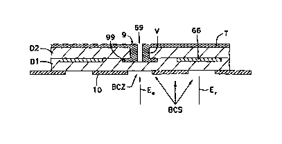
Referring to FIG. I, a cross-sectional view of a portion of one bead
transporter chuck
according to the present invention is shown. Stlvctures needed for a single
bead collection zone
are shown. The lower portion of this figure shows shield electrode 10 which is
applied to one
face of first dielectric layer Dl in a parallel plane using any number of
techniques known in the
art, such as laminating; powder deposition; or thin filin deposition, such as
magnetron sputtering
or electron beam evaporation. Dielectrics that may used include commonly
available materials
such as Corning Pyrex 7740 glass (high melting point borosilicate glass,
Corning Inc, Corning,
NY); a typical thickness is 10-20 mils. The shield electrode 10 is formed
having apertures (as
shown, by way of example). One such aperture allows for establishing a bead
collection zone
BCZ at the face of first dielectric layer Dl. Generally shield electrode 10,
and exposed portions
of first dielectric layer Dl form a bead contact surface BCS that is
accessible to bombardment,
contact or exposure to beads inside a bead dispenser or container, not shown.
In order to use
applied voltages to establish an attraction field Ee, as shown pointing to the
bead collection zone
BCZ, bead electrode 9 is provided.
Electric fields in this and later figures are shown using the standard
convention, showing
roughly the direction of the force on a positive test charge. However, for
actual examples of
applied voltages and bead transporter chuck operation in this disclosure, a
working convention is
adopted that negatively charged beads are to be attracted and later
discharged. When
manipulating positively charged beads, however, one may simply reverse the
applied voltages
from those given in the discussion below.
Bead electrode 9 comprises top portion T, via V, and center pad 99. A top
portion T of
bead electrode 9 is electrically connected to or integral with a center pad 99
by way of via V.
The illustrated center pad 99 is in a plane parallel with that of shield
electrode 10, but placed on
-9-
CA 02321007 2000-08-17
WO 99/42216 PCTNS99103575
the opposite side, or second face, of fizst dielectric layer Dl. This makes
center pad 99
inaccessible to the bead contact surface BCS or the bead collection zone BCZ.
The electric
field, however, generated by a potential applied to bead electrode 9 and
center pad 99 may
emanate through first dielectric layer Dl, with the net electric field
generated diminished by
electric polarization in first dielectric layer Dl, depending on its
dielectric constant E, which may
be anisotropic. See Classical Electrodynamics 2nd Ed., John David Jackson,
~1975, John
Wiley & Sons, New York.
The aperture in the shield electrode 10 at the bead collection zone BCZ may be
sized to
favor retention of beads of certain average diameters. A voltage may be
applied to bead
electrode 9 relative to another surface in the bead dispenser or container to
allow attraction of
beads to the bead contact surface BCS. Bead electrode 9 may serve to provide
an attraction field
for a plurality of bead collection zones, but only one bead collection zone is
shown here for
illustration. To aid in visual confirmation of bead capture at the bead
collection zone BCZ,
optional bead hole 69 is provided through bead electrode 9, via V, and center
pad 99 as shown.
For a transparent or translucent dielectric layer Dl, bead hole 69 provides a
visual or optical
monitor sight for whether a bead is retained. This allows for automated
verification of bead
occupancy in the bead collection zone, using known sensors to determine the
hole opacity in
terms of percent light transmission. For example, the light transmitted
through the bead holes 69
can be optically mapped onto an array detector such as a charge coupled device
(CCD), an
intensified CCD array, a focal plane array, a photodiode array or
photodetector array. The
array detector can be, for example, a CCD { such as that available from DALSA,
Inc. (Easton
CT), David Sarnoff Research Center (Princeton, NJ) or Princeton Instruments
(Trenton,
NJ) } , an intensified CCD array { such as that available from Princeton
Instruments,
Hamamatsu Corp. (Bridgewater, NJ) or Photometrics Ltd. of Tucson, AR}, a focal
plane
array { such as that available from Scientific Imaging Technologies, Inc.
(Beaverton, OR),
Eastman Kodak Co., Inc. {Rochester, NY) or David Sarnoff Research Center}, a
photodiode
array { such as that available from Reticon Corp. (Sunnyvale, CA), Sensors
Unlimited, Inc.
(Princeton, NJ) or Harnamatsu } or photodetector array { such as that
available from FLIR
Systems Inc. (Portland, OR), Loral Corp. (New York, NY), or Hughes Electronic
Corp. (Los
Angeles, CA)}.
In order to discourage beads from being attracted or retained at any locations
on the bead
contact surface BCS other than the intended bead collection zone BCZ,
repulsive field
- IO-
CA 02321007 2000-08-17
WO 99/42216 PCT/US99/03575
conductor 66 is provided as shown, which is illustrated as in the same plane
as, and surrounding,
center pad 99 of bead electrode 9. Apertures in shield electrode 10 as shown
allow a rejection
field E,. from repulsive field conductor 66 to emanate therethrough, after
passing through first
dielectric layer Dl. A optional second dielectric layer D2 is shown between
repulsive field
conductor 66 and top portion T of bead electrode 9. Via V passes from the top
portion T of
bead electrode 9 through this second dielectric layer D2 to center pad 99. In
lieu of either
second dielectric layer D2 or first dielectric layer Dl, or both layers, air
or the ambient gas or
vacuum may be used as a dielectric or insulator. This would expose one or both
of repulsive
field conductor 66 and bead electrode 9 directly to the bead contact surface.
Alternatively, first
dielectric layer Dl and second dielectric layer D2 may comprise one single
dielectric layer.
Fabrication techniques for forming conductive layers and electrodes in this
disclosure
may vary considerably, as any known technique satisfying modest electrical and
mechanical
requirements may be used. Nearly any metal may be used, for example, to form
repulsive field
conductor 66 and bead electrode 9, which may comprise thermally or
electromagnetically
deposited metals such as indium tin oxide, brass, platinum, copper, silver, or
gold, of any useful
thickness, but preferably about 1000 Angstroms to 10 microns ( 100,000
Angstroms). The same
is true for dielectric layers or laminates - the materials used may be of any
type compatible with
surrounding electrodes and conductors, and having sufficient dielectric
strength to withstand
anticipated voltages applied, including ceramic materials; silicon dioxide;
alumina; polyimide
resins and sheets or other suitable polymers; metallic oxides, such as
aluminum oxide and
titanium oxide; and titanates of calcium and magnesium.
Conductive vias such as via V may be of any convenient diameter that will
carry
anticipated electric currents during application and reduction of voltages,
preferably greater than
1000 Angstroms, which conveniently for example 50-75 microns in diameter or
about 100
microns or more where flexi-curcuit technology is used to fill the vias. Any
number of known
processes may be used to establish the vias, such as drilling by laser (such
as an excimer laser) or
etching (such as reactive ion etching including plasma-assisted etching with a
direction-
providing electrical field), or molding techniques. The use of photoresist
masks and related
techniques may be used to fill in or complete the conductive portion of a via
after drilling.
Materials used to complete or form the vias include metals such as spherical
gold powder that
are suspended in a carrier, such as liquid suspension of resins, solvents and
glass, forming a
conductive ink. Preferably this preparation is dried and fired after filling
to leave a solid plug of
-11-
CA 02321007 2000-08-17
WO 99/4ZZ16 PCTIUS99/03575
conductive material in each via. Regardless of fabrication technique, sizing
of via diameters
should not be so large as to interfere with other structures such as repulsive
field conductor 66 or
parts of bead electrode 9.
Now referring also to FIG. 2, a surface top view of the bead transporter chuck
of FIG.1
is shown, with the bead electrode 9 now shown configured for sixteen pixels or
bead collection
zones. Each bead collection zone is located in a parallel plane below the
plane of bead electrode
9. Each of the sixteen bead holes 69 shown is aligned with one of sixteen bead
collection zones,
not shown. An observer looking through bead holes 69 could see any retained
beads. Spacing
of the bead collection zones may vary, depending on the number and size of
beads to be
manipulated. For example, the entire surface of bead electrode 9 as shown,
with all sixteen
pixels or bead collection zones, may be a square of sides 49 mm in length; or
it may be much
smaller, say, 5 mm square, or 1.0 mm square, for manipulating small beads for
placement on a
smaller substrate, such as a pill or capsule.
Refernng also to FIG. 3, an auxiliary planar view of a bead transporter chuck
similar to
that of FIGS. 1 and 2 is shown, with the auxiliary view taken in the plane of
the repulsive field
conductor 66, and of the center pads 99. This view shows a bead transporter
chuck absent bead
hole 69 in bead electrode 9. Each center pad 99 coincides with, and provides
an attraction field
Es to, a bead collection zone. Notice that aside from openings surrounding and
proximate to
center pads 99, the repulsive field conductor 66 is continuous, serving to
discourage bead
retention outside of intended bead collection zones. First dielectric layer Dl
is shown in areas
not occupied by center pads 99 and repulsive field conductor 66.
Now referring to FIG. 4, a cross-sectional view similar to that of FIG. 1 is
given. A
portion of the bead transporter chuck of FIGS.1, 2, and 3 is shown, showing
structures that form
three bead collection zones. At the lower end of this figure is a bead
dispenser mesh (MESH)
shown at a distance D from the bead contact surface BCS. The bead dispenser
mesh may be a
mesh or a grid through which beads may pass for exposure to the bead
transporter chuck. The
bead dispenser mesh can also serve as a driving electrode or grid to
electrically propel charged
beads toward the bead contact surface of the bead transporter chuck. Any
number of mesh types
may be used, such as a # 270 mesh (Newark Wire Cloth Co Newark NJ) for
particles 4-6
microns diameter, or a # 200 mesh for particles of greater than 6 microns
diameter. The
structure shown is as above, with bead electrode 9 electrically connected to
three center pads 99
-12-
CA 02321007 2000-08-17
WO 99/42216 PC'f/US99/03575
by way of vias _V. Repulsive field conductor 66 is again present except in the
vicinity of center
pads 99.
Rough electric field lines representing E~ emanating from repulsive field
conductor 66
and Ea pointing toward center pad 99 of bead electrode 9 are shown, labeled
"E,. + Ee" and
showing field lines explicitly discouraging bead retention on areas of shield
electrode 10 or
exposed portions of first dielectric layer Dl that are not intended bead
collection zones.
Three beads and respective electric field Lines are shown for illustration. In
practice, one
introduces charged beads into the bead dispenser and the space shown between
the bead
dispenser mesh and the bead transporter chuck with its bead contact surface
BCS. For attracting
and retaining negatively charged beads, for example, one can apply a negative
bias to the bead
dispenser mesh (MESH), and a positive bias to the bead electrode 9, while a
negative bias
applied to repulsive field conductor 66 helps guide beads to their intended
destinations at the
bead collection zones BCZ.
In one embodiment, the shield electrode 10 is biased between the voltages
applied to the
bead electrodes 9 and the repulsive field conductors 66. This is conveniently
done by
connecting the shield electrodes to ground. This enhances user safety at the
bead contact
surface.
Available bead compositions are well known in the art, and are typically
polymer-based,
such as divinylbenzene copolymer; polystyrene; polyethylene glycol; or
polyethylene glycol graft
polystyrene, such as supplied under the trade name PEG-PS by PerSeptive
Biosystems of
Framingham, MA; or cross-linked polyethylene glycol resin, as supplied by Rapp
Polymer
GmbH of Germany. Beads may be dry, or may have absorbed or adsorbed an aqueous
solution,
or a fine powder. Beads can also be, for example, dry paint or phosphor
particles, or any other
powders that can be triboelectrically charged.
Beads may be charged prior to their application to the bead transporter chuck,
for
example, using plasma charging, or by the use of tribocharging (rubbing or
contact charging) as
known in the art. Materials that may be used for tribocharging include
polytetrafluoroethylene
('TEFLON°), and polymers of chlorotrifluorethylene, chlorinated
propylene, vinyl chloride,
chlorinated ether, 4-chlorostyrene, 4-chloro-4-methoxy-styrene, sulfone,
epichlorhydrin, styrene,
ethylene, carbonate, ethylene vinyl acetate, methyl methacrylate, vinyl
acetate, vinyl butyral, 2-
vinyl pyridine styrene, nylon and ethylene oxide. See, for example,
"Triboelectrification of
Polymers" in K.C. Frisch and A. Patsis, Electrical Properties of Polymers
(Technomic
-13-
CA 02321007 2000-08-17
WO 99/42216 PCT/US99/03575
Publications, Westport, CT), which is hereby incorporated by reference in its
entirety. Also see
Handbook of Electrostatic Processes, Jen-shih Chang, Arnold J. Kelly, and
Joseph M. Crowley,
eds., Marvel Dekker, Inc., New York, ~1995. For example,
polytetrafluoroethylene and
polyethylene and other materials that become negatively charged will tend to
create a positive
charge on the bead or object. Nylon and other materials that become positively
charged will
tend to create a negative charge on the bead or object. When using mechanical
shaking to
tribocharge polymer beads, it is preferred that the ratio of the amount or
mass of tribocharging
material used to charge the beads to the amount or mass of beads is such that
their respective
total surface areas are about equal.
Generally, there is a discrimination field due to the applied voltage Vp
applied between
the bead dispenser mesh or driving electrode (MESH) and the bead transporter
chuck, generally
at the bead electrode 9. For example, bead electrode 9 may be biased at + 1800
volts, and the
bead dispenser mesh at -1800 volts, for negatively charged beads. This gives
an applied voltage
Vp of 3600 volts total across distance D. This will function in sorting out
beads according to
polarity and chargelmass ratio, with beads of a certain charge/mass ratio and
con~ct polarity
being encouraged to seat themselves at the bead collection zones.
There is also electric polarization in the beads moving about the space
between the bead
dispenser mesh and the bead transporter chuck, giving rise to a polarization
field. We can sum
these fields, and refer to them simply as the polarization and discrimination
field, E~, whose field
lines are shown, labelled, "E~." The polarization and discrimination field
lines EP tend to point
to the center pad 99 of bead electrode 9, leaving a weak field region (Weak
Field Region) as
shown, at points where the rejection field Er cancels by superposition much of
the field EP.
For a charged bead with a charge/mass ratio q/m, the electrostatic force due
to the
polarization and discrimination field EP for improved bead guidance and
control should be
~9 _< ~a g (2)
that is, the polarization and discrimination field should not be sufficient in
itself to propel beads
to bead collection zones. This prevents too many beads from accumulating at
the bead
collection zones, clumping, etc.
The polarization and discrimination field, E~, is mostly determined by the
applied
voltage VP between the bead dispenser mesh and the bead transporter chuck
across an overall
distance D shown in Fig. 4,
EP ~ VP / D (3)
- 14-
CA 02321007 2000-08-17
WO 99/42216 PCTIUS99/03575
and EP should therefore be less than that required to lift the beads in the
absence of an amaction
field from any of the bead electrodes:
Ep < g / (q/m) (4)
Around the bead electrode and associated center pads 99, the rejection field
E,. from the
repulsive field conductor 66 is small, and so the total net electric field
strength is approximately
equal to the sum of the polarization and discrimination field EP and the bead
attraction field Ea:
Ecoc,, ~ EP + Ee (5)
and for bead capture and contml we should have
( Ep + Ea ) q > mn~a g (
only at the bead collection zones adjacent to bead electrode 9 and its
associated components.
However, once bead capture by the bead electrode at the bead collection zone
has
occurred, we should have
( EP + Ee ) q < ~a g (
to discourage more than one bead from being retained there. The magnitude of
the attraction
field E8 preferably drops back considerably after bead capture due to
geometric considerations,
aided by the fact that electric fields by their nature attenuate in an inverse
square relationship.
Naturally, in the bead population inside the bead dispenser there will be
variations in
both the mass of individual beads and in their respective charges. The
charge/mass ratio of the
beads is a determining factor in bead guidance and control, and for natural
stochastic processes,
the bead population distribution P(q/m) will be in the form of a Gaussian
distribution or bell
curve. In using the bead transporter chuck, one selects a certain minimum or
desired
(q/m)"".~,,o,~ with Ep and E8 chosen so that
EP _< g ~ (q/m)enr~a
but near an active bead electrode (with the attraction potential applied) we
should have, at the
same time:
( Es + EP ) > g ~ (q~m)cnr~n~a
The desired (q/m),~ can be experimentally determined to avoid having unduly
high bead
populations seeking and gaining retention at active bead electrodes, since a
single bead per bead
collection zone is the goal.
The bead transporter chucks according to the examples shown in FIGS. 1- 4
reduce
greatly the occurrence of wrongly charged beads being retained at bead
collection zones. They
rely on electrostatic attraction for bead guidance near the bead collection
zone, in addition to
-15-
CA 02321007 2000-08-17
WO 99/42216 PCT/US99/03575
using the polarization and discrimination field Ep. This minimizes the need
for acoustic aids in
coaxing beads to their intended locations for transport and later discharging.
With nv physically
exposed high voltages from either center pad 99, bead electrode 9 and via V,
or repulsive field
conductor 66, user safety is enhanced.
For beads having higher charge/mass ratios, such as porous or hollow beads, a
stronger
attraction field E8 relative to the polarization and discrimination field EP
is needed, along with a
less shielded rejection field E~ than before. Beads having higher chargelmass
ratios tend to
move too quickly, overwhelming the bead contact surface and making the
attraction and
placement of single beads difficult.
To address this need, another embodiment, an active field chuck, is
illustrated by way of
example in FIGS. 5, 6, 7, and 8, with similar structures as described above,
but using a bead
electrode 9 that is exposed to the bead contact surface and eliminating the
shield electrode 10.
Referring to FIGS. 5(a)-5(h), cross-sectional views of portions of bead
transporter
chucks according to the present invention are shown, in a format similar to
that of FIG. I, again
with structures shown that form one pixel or bead collection zone. In each of
the FIGS. 5(a)-
5(h), bead electrode 9 is shown, with top portion T as before, but with longer
vias V that extend
to to the bead contact surface BCS and form a bead collection zone on or near
the BCZ.
Dielectric layers Dl and D2 are shown as before, but now there is no shield
electrode 10 on the
bead contact surface of the bead transporter chuck. As before, repulsive field
conductor 66 is
continuous and planar, and applied to the other face of dielectric layer first
dielectric layer Dl.
As before, repulsive field conductor 66 also has apertures that allow an
attraction field Es to
point toward bead electrode 9 when a voltage is applied. Each bead electrode 9
again comprises
a top portion T which may be connected by known means to facilitate electrical
addressing.
Again, in lieu of either second dielectric layer D2 or first dielectric layer
Dl, or both layers, air or
the ambient gas or vacuum may be used as a dielectric or insulator. This would
expose one or
both of repulsive field conductor 66 and bead electrode 9 directly to the bead
contact surface.
Alternatively, first dielectric layer Dl and second dielectric layer DZ may
comprise one single
dielectric layer.
With the bead electrode 9 comprising a lower pad 89 or via V exposed to the
bead
contact surface, the active electric attraction field generated for a given
applied voltage is
stronger than for that of the bead transporter chuck of FIGS.1- 4. Also, the
exposed bead
electrode allows for active charging, where beads momentarily attracted there
end up losing or
- 16-
CA 02321007 2000-08-17
WO 99/42216 PCTIUS99/03575
gaining more charge (depending on the polarity of the charged bead) directly
to the bead
electrode 9. The only drawback is extra safety precautions needed due to
exposed high voltage.
'Ibis safety concern is attenuated since the capacitance of the system will
generally minimize
risk, and, furthermore, a current limiting resistor placed between the lower
pad 89 and the power
supply will further minimize any shock hazzard
In FIGS. 5(a), 5(c) and 5(e), bead electrode top portion T may be wide
relative to the
beads to be manipulated, say, ten times the average bead cross sectional area;
in other
embodiments of FIG. 5, the top portions T are not shown explicitly. In FIGS.
5(a), 5(b), S(c),
and 5(d), each via V of each bead electrode 9 is connected to a lower pad 89
that is exposed to
the bead contact surface and forms a bead collection zone. In FIGS. 5(e),
5(t~, 5(g), and 5(h),
each via V of each bead electrode 9 extends directly to the vicinity of the
bead contact surface to
form a bead collection zone, without use of a lower pad 89; in FIGS. S(e) and
5(~, the via V is
recessed somewhat from the bead contact surface, forming a nest of sorts for
the bead to be
attracted and retained. In FIGS. 5(c), 5(d), 5(e), 5(t7, 5(g), and 5(h), a
bead hole 69 is provided
in the central axis of each respective via V to act as a bead capture sight as
mentioned above.
Referring now to FIG. 6, an auxiliary planar view of the bead transporter
chuck
suggested by FIGS. 5(a) and 5(b) is shown, with the view taken in the plane of
the repulsive
field conductor 66, and with only one pixel or bead collection zone shown. Via
V of bead
electrode 9 is shown in the center of the aperture in repulsive field
conductor 66. Dielectric
material such as first dielectric layer Dl forms the balance of the aperture
in repulsive field
conductor 66.
FIG. 7 shows a similar view to that of FIG. 6, but with the auxiliary planar
view taken of
the bead transporter chuck suggested by FIGS. 5(c), 5(d), 5(e), 5(fj, 5(g) and
5(h). The figure
has an identical appearance to that of FIG. 6, except that a bead hole 69 is
visible in the center of
via V of bead electrode 9.
Referring now to FIG. 8, a cross-sectional view of a portion of a bead
transporter chuck
structurally similar to those shown in FIG. 5 is given. Structures forming
three bead collection
zones are shown, using a bead electrode 9 with vias V and lower pads 89 as
given in FIGS. 5(a)
and 5(b). Rough electric field lines for Es, Er, and Ep are shown as before in
above FIG. 4. The
polarization and discrimination field lines Ep tend to point to either the
lower pad 89 or the via V
of bead electrode 9, again leaving a weak field region (Weak Field Region) as
shown, at points
where the rejection field E,. cancels by superposition much of the field EP.
-17-
CA 02321007 2000-08-17
WO 99/42216 PCT/US99/03575
Overall, bead transporter chucks according to this invention use field
guidance so that
only around a bead collection zone and bead electrode 9 will the electric
fields be strong enough
to raise a bead from the bead dispenser or bead dispenser mesh and
subsequently guide it toward
the bead collection zone and optionally, bead hole 69. Once a bead lands
there, it weakens and
shields the electric field in the vicinity and no other beads are encouraged
to arrive there.
In the course of using the bead transporter chucks of this invention, a number
of
operating modes may be used. For bead pickup or retention, a bead electrode,
either exposed or
unexposed to the bead contact surface, is electrically biased to attract
beads, while the mesh of
the bead dispenser or other conductive surface is biased oppositely. Any
number of bead
electrodes 9 may be used, and they may be individually and separately
connected by known
means to facilitate individual and selective addressing in two dimensions. At
the same time, one
or more repulsive field conductors 66 may be either biased to the same
polarity as that of the
beads to be attracted, or simply grounded, depending on the sum of the
polarization and
discrimination field EP and attraction field Ee desired, as discussed above.
Repulsive field conductors such as shown by repulsive field conductor 66 are
electrodes
on the bead transporter chuck that function to generate electrical fields,
directly or indirectly that
discourage or merely deflect beads from being attracted, retained, at
locations other than bead
collection zones. Repulsive field conductors need not be explicitly repulsive,
that is, they do not
have to have the same charge polarity as the beads to be picked up and later
discharged. For
example, as mentioned, the repulsive field conductor may be held at ground
potential during
bead pickup. This may be aided by the effect of the dielectric surrounding the
repulsive field
conductor, where net repulsive surface charges will accumulate on the
repulsive field conductor
in response to a charged bead in the vicinity.
During bead pickup, the shield electrode 10 of the embodiments described in
F1GS.1- 4
may be held at ground potential as well. However, it may be biased to a charge
polarity similar
to that of the desired beads. The shield electrode 10 then becomes a repulsive
field conductor.
In the embodiments described in FIGS.1- 4, this is tantamount to having an
additional repulsive
field conductor 66 exposed to the bead contact surface.
However, even when grounded and not acting in an explicitly repulsive manner,
shield
electrodes are useful, helping to define and shape the attraction field E8 set
up by the bead
electrodes, particularly because the attraction field would otherwise be
shaped instead by any
dielectric material used surrounding the bead electrode, such as first
dielectric layer Dl. Shield
-18-
CA 02321007 2000-08-17
WO 99142216 PCT/US99/03575
electrode 10 may be allowed to "float," not biased or grounded. Generally
however, grounded or
not, good results are obtained when the shield electrodes are biased at a
voltage between that
applied to the bead electrodes) 9 and that applied to the bead dispenser mesh
(MESH).
In one embodiment, the bead transporter chuck described in FIGS.1- 4 may be
used.
An bead electrode 9 may be fabricated by depositing, using known techniques,
such as using a
5000 Angstrom layer of gold (Au) onto the second dielectric layer D2.
Alternatively, bead
electrode 9 may comprise a 100 Angstrom layer of chromium (Cr) and with a 5000
Angstrom
gold (Au) overcoat. Second dielectric layer D2 may be made of Dupont~ Kapton~
polyimide
film (type 300 HN, 3 mil thickness) or on Corning Pyrex 7740 glass of I O mils
thickness.
Center pads 99 and repulsive field conductor 66 may comprise a 35 micron
deposition of copper
(Cu) onto first dielectric layer Dl. A similar deposition to form the shield
electrode 10 may be
applied to the opposite face of the first dielectric layer Dl, with apertures
being about ten times
the diameter of the beads to be manipulated.
A bead dispenser container containing this bead transporter chuck is then
filled with 270
I 5 micron diameter negatively precharged Merrifield beads. A potential of -
1800 V is applied to
the bead dispenser mesh, + 1800 V to the bead electrode 9, and the repulsive
field conductor 66
is grounded, set to 0 volts. ('This assumes that the desired bead species is
negatively charged, or
that one is exploiting a polarization-induced negative surface charge on a
bead. ff a positively
charged bead or a positive surface charge is to be used, then these polarities
may be reversed.)
No wrongly placed beads were observed for adequate distances D between the
bead dispenser
mesh and the bead transporter chuck, that is D from about I/4" (6 mm) to 1"
(25 mm). For
smaller distances D, accuracy diminishes.
In another embodiment, the bead transporter chuck as shown in FIGS. 5 - 8 may
be used,
using similar fabrication, but with no shield electrode 10 and having exposed
bead electrodes 9.
A bead dispenser containing this bead transporter chuck is then filled with
270 micron diameter
negatively precharged Merrifield beads. Excellent results are again obtained,
using lower
potentials: a potential of - 800 V is applied to the bead dispenser mesh
(MESH), + 800 V to the
bead electrode 9, and the repulsive field conductor 66 is grounded, set to 0
volts. A lower
voltage requirement is thus verified for this embodiment.
In each case, applied voltages cause bead electrode 9 to attract and retain
beads, with
single beads on each bead collection zone. Beads on the bead transporter chuck
are optionally
transported to a substrate, microtiter plate, or other destination by moving
the entire bead
- 19-
CA 02321007 2000-08-17
WO 99/4ZZ16 PCT/US99103575
transporter chuck, or alternatively, the target substrate or plate is brought
to the chuck. Beads
are then released or discharged in a controlled manner when the applied
voltages, such as those
given above, are reversed or set to zero. Alternatively, for bead release,
only the bead electrode 9
may be shorted out or grounded (0 volts), or have an opposite voltage applied.
Optionally, when
shield electrode 10 is used, it may be biased to be repulsive to beads during
bead discharge.
When using bead transporter chucks according to the present invention, the
temperature
is preferably between - 50°C and 200°C, and more preferably
between about 22°C and 60°C.
Relative humidity may be 0 - 100 percent, so long as condensation does not
occur, more
preferably the relative humidity is about 30 percent.
Bead holes 69 are typically lined up with, but not necessarily coincident with
the bead
collection zones. There may be multiple bead collection zones for each
independently controlled
bead electrode 9. The dielectric layers used allow safety, and electrical
isolation between
electrodes and conductors. They also reduce fields produced by applied
voltages and allow
retention of beads containing a higher net charge. 1n addition, they can also
provide structural
rigidity and strength to the bead transporter chuck. For preparation of
administration forms,
precision achieved is high and repeatable, as beads taking the form of
microspheres may, in one
embodiment, be 1 to 500 microns in diameter, preferably about 50 microns.
By using an appropriate configuration of cyclic or repeating strong repulsive
field
components in the bead transporter chuck -- that is, repulsive field
conductors or shield
electrodes biased to become repulsive field conductors -- beads are field-
guided to bead
collection zones. The attraction field Ee is substantially reduced once a bead
has been picked
up, since the bead acts as a shield. Thus, single bead occupancy in each of
the individual pixels
or elements of the bead collection zone is achieved, with virtually no
occurrence of wrongly
charged beads at the bead electrodes. An advantage to the use of repulsive
field conductors is
that they can act as sinks or holding sites for wrongly charged beads that
might otherwise make
unwanted moves into a bead collection zone.
Bead electrodes 9 may comprise any number of separately addressable pixels or
elements
in two directions x and y, each having separately controlled bead collection
zones. Any number
of well known means and structures may be used to facilitate addressing as is
known in the
electrical and electronic arts, where top portion T previously described in
FIGS. 1, 4, 5(a)-(h),
and 8 may comprise a bus or address lead. In this way, combinational synthesis
or analysis may
be simplified as discussed above. In using the bead transporter chucks, one
may expose the bead
-20-
CA 02321007 2000-08-17
WO 99/42216 PCT/US99/03575
contact surface of such a chuck to beads; selectively apply voltages, such as
the voltages given
above, for each x-y addressable well, pixel, or individual spatial element of
the chuck, to attract
and retain beads selectively at each bead collection zone; then release the
beads onto a desired
destination aligned with the bead transporter chuck by selectively reversing
or reducing voltages
S associated with each bead collection zone as required.
It is also possible that beads attracted by the chuck, especially large
diameter beads or
objects of large overall size, say 3 mm in diameter, may by known process
design become
substrates, to be coated with a pharmaceutically active compound. Such beads
could include
oblong shapes, made of water soluble filin, such as hydroxypropyl methyl
cellulose resin. See
US Patent Application Serial No. 08/471,889, "Methods and Apparatus for
Electronically
Depositing a Medicament Powder Upon Predefined Regions of a Substrate," filed
June 6, 1995,
and continuation-in-part thereof filed June 6, 1996, Serial No. 08/659,501,
which documents are
incorporated herein by reference in their entirety.
In this way, electrostatic chucks can be scaled up for large scale continuous
manufacturing, such as using a sheet of an edible substrate for use with
tablets, for example, or a
sheet of an inhaler substrate. For example, hydroxypropyl methyl cellulose can
be used, such as
Edisol M Film M-900 or EM 1100 available from Polymer Films Inc. (Rockville
CIA. One
advantage using bead transporter chucks according to this invention,
especially the active field
embodiments shown in FIGS. 5 - 8, is that with an exposed bead electrode 9 the
chuck can
maintain the charge of a pharmaceutical substrate that would otherwise lose
its charge.
Generally, sizing of bead diameters may range from less than one micron to
1000 microns or
larger; 1 SO microns is fairly typical.
Obviously, many modifications and variations of the present invention are
possible in
light of the above teaching. It is therefore to be understood, that within the
scope of the
appended claims, the invention may be practiced otherwise than as specifically
described or
suggested here.
-21 -