Note: Descriptions are shown in the official language in which they were submitted.
CA 02321128 2000-09-26
-1-
SPECIFICATION
LIGHT RESPONSIVE SEMICONDUCTOR SWITCH WITH SHORTED LOAD
PROTECTION
BACKGROUND OF THE INVENTION
1. Field of the Invention
The present invention relates to a light responsive semiconductor switch with
shorted load protection for use in an optical relay.
2. Description of the Prior Art
Japanese Patent Publication No. 11-163706 discloses a light responsive
semiconductor switch for use in an optical relay. The switch includes a
photovoltaic element which provides an operating voltage upon absorption of
light from a light source, and an output transistor which is triggered by the
operating voltage to become conductive for connecting a load to a power
source.
In order to protect the output transistor from an overcurrent due to an
accidental
short-circuiting of the load, the switch includes an overcurrent sensor for
detection of the overcurrent condition, and a shunt transistor which, in
response
to the overcurrent condition, becomes conductive to flow the current from the
2o photovoltaic element away from the output transistor to turn if off for
interruption
of the overcurrent. Further, the switch includes a latch circuit which, in
response
to the overcurrent condition, provides and holds an interruption signal fed to
a
control electrode of the output transistor to keep turning off the output
transistor
for continued interruption of the overcurrent. In this prior art, the shunt
transistor
is included in the latch circuit to be responsible also for the latching
operation.
CA 02321128 2000-09-26
-2-
Therefore, the shunt transistor has to satisfy two different requirements, one
for
the turning off of the output transistor, and the other for holding the
interruption
signal applied to the control electrode of the output transistor in
association with a
resistor in the latch circuit. With this restriction to the shunt transistor
common
to the latch circuit, it is rather difficult to combine the two requirements
against
the use of the photovoltaic element of varying current generating capacity.
For
example, when the photovoltaic element having a large current generating
capacity is used to apply a correspondingly high voltage to the control
electrode
of the output transistor for rapidly turning it on, the conduction of the
shunt
transistor made for the latching operation may not be enough to lower the
voltage
applied to the control electrode of the output transistor below a threshold
voltage
thereof, failing to turn ofif the output transistor even when the shunt
transistor is
made conductive to draw the current from the photovoltaic element.
Accordingly,
the prior switch poses limitations to a circuit design and is not satisfactory
for
complete interruption of the overcurrent irrespective of the current
generating
capacity of the photovoltaic element.
SUMMARY OF THE INVENTION
In view of the above insufficiency in the prior art, the present invention has
been achieved to provide an improved light responsive semiconductor switch
2o with shorted load protection which is capable of successfully interrupting
a load
overcurrent. The semiconductor switch in accordance with the present invention
comprises an output switching transistor connected between a pair of output
terminals which are adapted for connection to a load circuit composed of a
load
and a power source energizing the load. The output switching transistor has a
control electrode with a threshold voltage at which the output switching
transistor
CA 02321128 2000-09-26
-3-
conducts to connect the load to the power source. A photovoltaic element is
included in the switch to generate an electric power upon absorption of light
from
a light source. The electric power provides an operating voltage decreasing
with
an increasing current flowing from the photovoltaic element. An overcurrent
sensor is coupled to the load circuit to provide an overcurrent signal when
the
load circuit sees an overcurrent flowing through the load from the power
source.
A shunt transistor is connected in series with a current limiting resistive
element
across the photovoltaic element to define a shunt path of flowing the current
from
the photovoltaic element through the current limiting resistive element away
from
1o the output switching transistor. Also included in the switch is a latch
circuit
which is connected to the overcurrent sensor and the shunt transistor. The
latch
circuit is energized by the photovoltaic element and provides an interruption
signal once the overcurrent signal is received and holds the interruption
signal
after the removal of the overcurrent signal. The interruption signal causes
the
~5 shunt transistor to become conductive to flow the current from the
photovoltaic
element through the shunt path, lowering the operating voltage being applied
to
the control electrode of the output switching transistor below the threshold
voltage so as to turn off the output switching transistor for disconnection of
the
load from the power source.
2o The characterizing feature of the present invention resides in that the
shunt
transistor and the current limiting resistive element are formed separately
from
the latch circuit, and that the current limiting resistive element is
connected
between the control electrode of the output switching transistor and the
positive
electrode of the photovoltaic element so as to limit the current from the
25 photovoltaic element, when said shunt transistor is conductive, to such an
extent
CA 02321128 2000-09-26
-4-
as to lower the operating voltage being applied to the control electrode of
the
output switching transistor below the threshold voltage, while allowing the
photovoltaic element to provide a supply voltage to the latch circuit for
holding the
interruption signal. Thus, the series combination of the current limiting
resistive
element and the shunt transistor which are separately formed from the latch
circuit can assure to provide the supply voltage to the latch circuit and at
the
same time to limit the operative voltage being applied to the control
electrode of
the output switching transistor, so as to keep the interruption signal from
the latch
circuit on one hand, and to turn off the output switching transistor without
fail in
1o response to the interruption signal on the other hand, enabling successful
and
reliable interruption of the overcurrent. Also, since the current limiting
resistive
element is separately formed from the latch circuit, it is readily possible to
assure
the above interruption of the overcurrent irrespective of varying current
generating capacity of the photovoltaic element, simply by selecting the
impedance of the current limiting resistive element. With this result, the
output
transistor can be protected completely from the overcurrent in the load
circuit.
In one version of the present invention, the overcurrent sensor is realized by
a current sensing resistor inserted in the load circuit, and a transistor
switch
which is disposed to receive a voltage developed across the current sensing
2o resistor to provide the overcurrent signal to the latch circuit when the
voltage
exceeds a predetermined level.
In another version of the present invention, the overcurrent sensor is
realized
by. a current sensing resistor connected in series with a bypass switching
transistor between the output terminals and in parallel with the output
switching
transistor, and a transistor switch which is disposed to receive a voltage
CA 02321128 2000-09-26
-5-
developed across the current sensing resistor to provide the overcurrent
signal to
the latch circuit when the voltage exceeds a predetermined level.
For driving the load energized the DC power supply, the output switching
transistor is preferably defined by a single metal oxide semiconductor field-
effect
transistor (MOSFET) whose gate-source is connected across the photovoltaic
element, and whose drain-source is connected between the output terminals.
For driving the load energized by the AC power supply, the switch is
preferred to include a pair of output switching transistors each in the form
of a
metal oxide semiconductor field-effect transistor (MOSFET). The two output
1o switching transistors are connected in series between the output terminals
with
sources of the individual MOSFETs being connected to each other and with gates
of the individual MOSFETs being commonly connected to receive the operating
voltage from the photovoltaic element.
Preferably, the latch circuit is realized by a flip flop having a set input, a
reset
input, and an output. The set input is connected to receive the overcurrent
signal and the reset input is connected to receive the operating voltage from
the
photovoltaic element, while the output is connected to turn on and off the
shunt
transistor.
The shunt transistor is preferred to be a metal oxide semiconductor
2o field-effect transistor (MOSFET) whose drain-source is connected in series
with
the current limiting resistive element across the photovoltaic element. In
this
connection, the flip-flop is realized by a combination of a first resistive
element
and a first metal oxide semiconductor field-effect transistor (MOSFET) whose
drain-source is connected in series with the first resistive element across
the
photovoltaic element, and a combination of a second resistive element and a
CA 02321128 2000-09-26
-6-
second metal oxide semiconductor field-effect transistor (MOSFET) whose
drain-source is connected in series with the second resistive element across
the
photovoltaic element. The first MOSFET has a gate connected to a point
between the second resistive element and a drain of the second MOSFET. The
second MOSFET has a gate connected to a point between the first resistive
element and a drain of the first MOSFET. The point between the second
resistive element and the drain of the second MOSFET is also connected to the
gate of the shunt transistor (MOSFET) so as to provide the interruption signal
to
the gate of the shunt transistor. The second MOSFET receives at its gate the
operating voltage from the photovoltaic element through the first resistive
element so as to become conductive, thereby lowering the operating voltage
applied through the second resistive element to the gate of the first MOSFET
and
to the gate of the shunt transistor (MOSFET) to make the first MOSFET and the
shunt transistor (MOSFET) non-conductive, thereby applying the operating
voltage to the control electrode of the output switching transistor to turn it
on.
The second MOSFET also receives at its gate the overcurrent signal which
makes the second MOSFET nonconductive, thereby raising the voltage applied
to the gates of the first MOSFET and the shunt MOSFET so as to make the first
MOSFET and the shunt transistor (MOSFET) conductive, which keeps the
2o second MOSFET non-conductive for continued conduction of the shunt
transistor
(MOSFET) for keeping the interruption of the output switching transistor until
removal of the operating voltage from the photovoltaic element.
For the above circuit configuration, each of the current limiting resistive
element, the first resistive element and the second resistive element is
preferably
in the form of a punch-through space charge resistor. The punch-through space
CA 02321128 2000-09-26
7_
charge resistor is realized by a semiconductor substrate having a conductive
type
which is one of n-type and p-type, a well diffused in the surface of the
substrate
and being of a conductive type opposite of the substrate, and a pair of
regions
diffused in the surface of the well in a spaced relation with each other. The
regions are of the same conductive type as the substrate. Electrodes are
respectively formed on the regions to apply the operating voltage between the
regions partly through the well. In this condition, the regions are
cooperative to
form therebetween a depletion layer responsible for carrying a minute current
and therefore defining resistance for each of the current limiting resistive
element,
1o the first resistive element and the second resistive element. Since the
punch-through space charge resistor can realized into a micro structure while
exhibiting a high resistance, the whole switch can be made compact even when
the photovoltaic element of small current generating capacity is utilized to
require
a considerably high resistance for each resistive element.
Alternatively, the current limiting resistive element, the first resistive
element
and the second resistive element may be realized by diodes, respectively.
Preferably, the output switching transistor is realized by a metal oxide
semiconductor field-effect transistor (MOSFET) having a gate defining the
control
electrode. A zener diode is connected across gate-source of the output
2o switching transistor in parallel with the photovoltaic element in such a
manner as
to connect a cathode of zener diode to the gate of the output switching
transistor.
The zener diode is selected to have a breakdown voltage higher than an
open-circuit voltage of the photovoltaic element. Thus, even when an
excessively large voltage is applied to the output switching transistor due to
the
2s load short circuit, the zener diode can clamp the gate voltage of the
output
CA 02321128 2000-09-26
_$_
switching transistor to the breakdown voltage so as to protect the output
transistor from destructive voltage.
A diode may be being connected across the current limiting resistive element
with an anode of the diode connected to the gate of the output switching
transistor. Thus, when the photovoltaic elements is turned off to cease
providing
the operating voltage, the diode establishes a bypass across the current
limiting
resistive element for discharging the charges accumulated in the gate of the
output switching transistor, thereby speeding up the discharge to rapidly turn
off
the output switching transistor.
1o In this connection, a resistor may be connected in series with the diode
across the current limiting resistive element in order to avoid malfunction of
the
short-circuit interruption of the switch when the load circuit is subjected to
a high
voltage noise such as a lightning surge. Upon occurrence of the high voltage
noise while the output switching transistor is kept turned on, a rushing
current
~5 would flow from the drain to the gate of the output switching transistor
(MOSFET)
through a parasitic capacitance in the drain-gate path into the photovoltaic
element, thereby instantaneously canceling the operating voltage of the
photovoltaic element. If this should occur, the latch circuit would be reset
to turn
off the shunt transistor, disabling the interruption of the overcurrent in the
load
2o circuit, failing to protect the load circuit as well as the output
switching transistor.
However, the resistor included in the above bypass can well delimit the
rushing
current to avoid the unintended reset of the latch circuit and assure a safe
protection of interrupting the overcurrent against the high voltage noise.
Instead of the diode connected across the current limiting resistive element,
a
25 discharging metal oxide semiconductor field-effect transistor (MOSFE'i7 may
be
CA 02321128 2000-09-26
_9_
utilized for the same purpose of rapidly turning off the output switching
transistor
in response to the deactivation of the photovoltaic element. The discharging
MOSFET has a source coupled to a connection between the current limiting
resistor element and the positive electrode of the photovoltaic element and
has a
drain and a gate which are commonly connected to the gate of the output
switching transistor for discharging the charge accumulated in the gate of the
output switching transistor through the MOSFET when the photovoltaic element
is deactivated.
Preferably, the transistor forming the overcurrent sensor is realized by a
third
1o metal oxide semiconductor field-effect transistor (MOSFET) which provides
the
overcurrent signal to the latch circuit upon being turned on. In this
connection,
an additional photovoltaic element may be used to provide an offset voltage,
upon absorption of the light, which is added to a detected voltage appearing
across the current sensing resistor. The additional photovoltaic element is
connected in circuit to the third MOSFET so as to turn on the third MOSFET
when the detected voltage plus the offset voltage exceed a predetermined
level.
Thus, even a relatively low detection voltage across the current sensing
resistor
can successfully trigger the third MOSFET for increasing sensitivity of the
third
MOSFET or the overcurrent sensor to the overcurrent condition. Therefore, the
2o third MOSFET can well respond to a low level overcurrent for successfully
protecting the output switching transistor therefrom.
In another version of the present invention, the switch further includes a
second shunt transistor in the form of a metal oxide semiconductor field-
effect
transistor (MOSFET) connected across the shunt transistor. The second shunt
transistor has a drain which is connected to a point between the control
electrode
CA 02321128 2000-09-26
-10-
of the output switching transistor and the current limiting resistive element,
and
has a source which is connected to the source of the shunt transistor. The
second shunt transistor has a gate which is connected to directly receive the
voltage developed across the current sensing resistor such that, in response
to
the voltage of the current sensing resistor exceeding the predetermined level,
the
second shunt transistor becomes conductive to flow the current from the
photovoltaic element through the current limiting resistive element and
through
the second shunt transistor away from the output switching transistor prior to
the
latch circuit responding to provide the interruption signal of turning on the
shunt
1o transistor. With this arrangement, the output switching transistor can be
turned
off for interruption of the overcurrent in prompt response to the overcurrent
condition without having to wait for the actuation of the latch circuit, and
can be
held turned off by the subsequently actuated latch circuit. Thus, it is
readily
possible to give a more reliable protection of the output switching transistor
even
~5 against an instantaneous overcurrent flow.
The switch may include a biasing means for supplying a bias current from the
photovoltaic element to the gate of the shunt transistor when the latch
circuit
provides the interruption signal in response to the overcurrent signal. With
the
addition of the bias current or the bias voltage to the gate of the shunt
transistor,
2o the shunt transistor can be promptly triggered to turn on for rapid
interruption of
the overcurrent through the output switching transistor, thereby protecting
the
output switching transistor as well as the associated element effectively.
Also, the switch may include a block circuit for blocking the current of the
photovoltaic element from flowing to the gate of the output switching
transistor
25 when the latch circuit provides the interruption signal in response to the
CA 02321128 2000-09-26
-11 -
overcurrent signal. With the inclusion of the blocking circuit, the current
from the
photovoltaic element is intensively utilized for triggering the shunt
transistor,
thereby quickening the interruption of the overcurrent for immediate
protection of
the output switching transistor against the overcurrent.
Further, the overcurrent sensor may include a low-pass filter which negates
or cancel a high frequency voltage appearing across the current sensing
resistor
so that the overcurrent sensor provides the overcurrent signal to the latch
circuit
only when the voltage across the current sensing resistor exceeds the
predetermined level and lasts over a certain time period. Thus, the latch
circuit
io is prevented from providing the interruption signal in response to
noncritical
overcurrent appearing only instantaneously in the load circuit such as minor
noises and rushing current which does not require the protection of the output
switching transistor.
Moreover, the switch may include a delay timer which delays providing the
overcurrent signal from the overcurrent sensor to the latch circuit for a
short time
period immediately upon the photovoltaic element generating the electric
power,
thereby canceling a transient voltage appearing across the current sensing
resistor immediately after the activation of the photovoltaic element. With
the
inclusion of the delay timer, the output switching transistor can be prevented
from
2o responding to noncritical overcurrent appearing immediately after the
actuation of
the photovoltaic element for assuring reliable switching operation.
These and still other objects and advantageous features of the present
invention will become more apparent from the following description of the
embodiments when taken in conjunction with the attached drawings.
CA 02321128 2000-09-26
-12-
BRIEF DESCRIPTION OF THE DRAWINGS
FIG. 1 is a circuit diagram of a light responsive semiconductor switch with
shorted load protection in accordance with a first embodiment of the present
invention;
FIG. 2 is a sectional view illustrating a punch-through space charge resistor
utilized in the above switch;
FIG. 3 is a sectional view illustrating a diffused resistor utilized in the
above
switch;
FIG.4 is a semiconductor switch in accordance with a second embodiment of the
io present invention;
FIG. 5 is a circuit diagram in accordance with a first modification of the
first
embodiment;
FIG. 6 is a circuit diagram in accordance with a second modification of the
first
embodiment;
i5 FIG. 7 is a circuit diagram of a light responsive semiconductor switch in
accordance with a third embodiment of the present invention;
FIG. 8 is a circuit diagram of a light responsive semiconductor switch in
accordance with a fourth embodiment of the present invention;
FIG. 9 is a circuit diagram of a light responsive semiconductor switch in
2o accordance with a fifth embodiment of the present invention;
FIG. 10 is a circuit diagram of a light responsive semiconductor switch in
accordance with a sixth embodiment of the present invention;
FIG. 11 is a circuit diagram illustrating a first modification of the sixth
embodiment;
25 FIG. 12 is a circuit diagram illustrating a second modification of the
sixth
CA 02321128 2000-09-26
-13-
embodiment;
FIG. 13 is a circuit diagram of a light responsive semiconductor switch in
accordance with a seventh embodiment of the present invention;
FIG. 14 is a circuit diagram illustrating a modification of the seventh
embodiment;
s FIG. 15 is a circuit diagram of a light responsive semiconductor switch in
accordance with an eight embodiment of the present invention;
FIG. 16 is a circuit diagram illustrating a modification of the eighth
embodiment;
FIG. 17 is a circuit diagram of a light responsive semiconductor switch in
accordance with a ninth embodiment of the present invention;
FIG. 18 is a circuit diagram illustrating a modification of the ninth
embodiment;
and
FIG. 19 is a circuit diagram illustrating a third modification of the first
embodiment.
15 DETAILED DESCRIPTION OF THE EMBODIMENTS
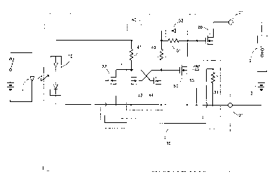
First Embodiment <FIG. 1 >
Referring now to FIG. 1, there is shown a light responsive semiconductor
switch in accordance with a first embodiment of the present invention. The
switch is utilized in combination with a light emitting diode 1 to constitute
an
20 optical relay for connecting and disconnecting a load 2 to and from its
power
source 3. The switch includes a photovoltaic element 10 in the form of a
photo-diode array which generates an electric power upon absorption of a light
from the light emitting diode 1. The electric power gives an operating voltage
which decreases with an increasing current from the photo-diode array 10. The
25 operating voltage is applied to trigger an output switching transistor 20
in the form
CA 02321128 2000-09-26
-14-
of an n-channel enhancement metal oxide field-effect transistor (MOSFET)
whose gate-source is connected across the photo-diode array 10. The output
MOSFET 20 has a drain and a source connected respectively to output terminals
21 which are adapted in use for connection with a load circuit composed of the
load 1 and the power source 3. The gate of output MOSFET 20 is connected to
receive the operating voltage from the photo-diode array 10 so that, output
MOSFET 20 becomes conductive, in response to the activation of the
photo-diode array 10, for connection of the load 2 to the power source 3. In
order to protect the switch, particularly the output MOSFET 20 from being
1o damaged by an overcurrent which may flow through the load circuit due to an
accidental short-circuiting of the load, the switch includes an overcurrent
sensor
30, a latch circuit 40, and a shunt transistor 50 which are cooperative to
keep the
output MOSFET 20 turned off for interruption of the overcurrent once the
overcurrent condition occurs.
The overcurrent sensor 30 is composed of a current sensing resistor 31
connected between the source of output MOSFET 20 and the output terminal 21,
and a MOSFET 32 whose gate is connected to receive a detection voltage
across resistor 31 so as to become conductive when the detection voltage
exceeds a predetermined level indicative of the overcurrent. MOSFET 32 has a
2o drain connected through a first resistor 41 to a positive electrode of the
photo-diode array 10 and has a source connected to a negative electrode of the
photo-diode array 10.
The latch circuit 40 is in the form of a flip-flop composed of a series
combination of the first resistor 41 and a first MOSFET 42 connected across
the
photo-diode array 10, and a series combination of a second resistor 43 and a
CA 02321128 2000-09-26
-15-
second MOSFET 44 across the photo-diode array 10. The first MOSFET 42
has its gate coupled to a connection between the second resistor 43 and a
drain
of the second MOSFET 44, while the second MOSFET 44 has its gate coupled to
a connection between the first resistor 41 and a drain of the first MOSFET 42.
The shunt transistor 50 is also a MOSFET whose drain-source is connected in
series with a current limiting resistor 51 across the photo-diode array 10 and
is
connected across gate-source of the output MOSFET 20. The shunt MOSFET
50 has a gate coupled to the connection between the second resistor 43 and the
drain of the second MOSFET 44. The latch circuit 40 is configured such that,
1o upon activation of the photo-diode array 10, the second MOSFET 44 is first
to
become conductive, thereby lowering voltage applied to the gates of the first
MOSFET 42 and the shunt MOSFET 50 to keep the MOSFETs 42 and 50
non-conductive. When MOSFET 32 becomes conducive in response to the
overcurrent condition, the second MOSFET 44 becomes non-conductive to
thereby make the first MOSFET 42 and the shunt MOSFET 50 conductive,
thereby drawing the current from the photo-diode array 10 through the shunt
MOSFET 50 away from the output MOSFET 20 and therefore turning off the
output MOSFL~'1' 50 for interruption of the overcurrent in the load circuit.
This
condition is kept until the photo-diode array 10 is deactivated. In this
sense, the
latch circuit 40, i.e., the flip flop has set input defined at the connection
between
the first resistor 41 and the first MOSFET 42 to receive an overcurrent signal
which is caused by the conduction of MOSFET 22 upon occurrence of the
overcurrent condition. The flip-flop has a rest input defined at a connection
between the first resistor 41 and the positive electrode of the photo-diode
array
10 to receive the operating voltage from the photo-diode array 10, while the
CA 02321128 2000-09-26
flip-flop has an output defined at the connection between the second resistor
43
and the second MOSFET 44 to issue an interruption signal to the gate of the
shunt MOSFET 50 once MOSFET 32 applies the overcurrent signal to the set
input. Thus, the interruption signal is held until the switch is reset by
deactivation of the photo-diode array 10.
The current limiting resistor 51 is inserted between the gate of the output
MOSFET 20 and the positive electrode of the photo-diode array 10 at such a
location as to limit a shunt current flowing through the shunt MOSFET from the
photo-diode array 10 when the latch circuit 40 operates to provide the
interruption
1o signal, thereby affording a sufficient voltage being applied to the latch
circuit 40
from the array 10, whereby the latch circuit 40 is kept energized by the array
10
to continue providing the interruption signal.
A diode 52 is connected across the resistor 51 with its anode coupled to the
gate of the output MOSFET 20 to establish a bypass across the resistor for
releasing the electrical charge accumulated in the gate of the output MOSFET
20
when the array 10 is deactivated, thereby speeding up the discharge for rapid
turn off of the output MOSFET. A zener diode 53 is connected across
gate-source of the output MOSFET 20 with a cathode of zener diode 53
connected to the gate of output MOSFET 20. The zener diode 53 is also
2o connected across the photo-diode array 10 and has a breakdown voltage
higher
than an open-circuit voltage of the array 10. When an excessively large
voltage
is applied to the output MOSFET 20 due to the short-circuiting of the load,
the
zener diode 53 clamps the gate voltage of output MOSFET 20 to the breakdown
voltage for protecting it from destructive voltage.
Referring now to FIG. 2, there is shown a punch-through space charge
CA 02321128 2000-09-26
-17-
resistor element utilized for the resistors 41, 43, and 51 of the circuit of
FIG. 1.
The punch-through space charge resistor is formed in a semiconductor substrate
60 of n-type or p-type. A well 61 of the conductive type opposite of the
substrate is diffused in the surface of the substrate 60, and a pair of
regions 62 of
the same conductive type as the substrate are diffused in the surface of the
well
61 in a spaced relation with each other. Formed respectively on the regions 62
are electrodes 63 which apply the operating voltage between the regions partly
through the well. With the application of the operating voltage, the regions
62
are cooperative to form therebetween a depletion layer 64 responsible for
1o carrying a minute current and therefore defining resistance of high
resistance.
Thus configured punch-through space charge resistor can realized into a micro
structure while exhibiting a high resistance. Therefore, the whole switch can
be
made compact when the photo-diode array 10 of small current generating
capacity is utilized to require a considerably high resistance for each of the
resistors 41, 43, and 51.
FIG. 3 shows a diffused resistor which may be utilized as an alternative
resistive element for an alternative resistive element which may be utilized
as the
resistors 41, 43, and 51. The diffused resistor comprises a semiconductor
substrate 65 of n-type or p-type, a well 66 of opposite conductive type, and a
2o region 67 of the same conductive type as the substrate diffused in the
surface of
the well 66. With the well 66 being grounded to earth, the region 67 serves as
a
resistive element of high resistance. Thus, the high resistance can be
achieved
with a microstructure to make the switch compact.
Second Embodiment <FIG. 4>
2s Referring to FIG. 4, there is shown a light responsive semiconductor switch
in
CA 02321128 2000-09-26
_ 1g
accordance with a second embodiment of the present invention. The switch of
this embodiment is designed for a load circuit of energizing the load 2 with
an AC
power source 3A, and is identical to the first embodiment except for the use
of an
additional output MOSFET 22 and for the inclusion of an additional current
sensing resistor 33, and an additional sensor MOSFET 34 in the overcurrent
sensor 30A. Like elements are designated by like reference numerals with a
suffix letter of "A". The additional output MOSFET 22 is connected in series
with
the output MOSFET 20A between the output terminals 21 A with the sources of
MOSFETs 20A and 22 being connected to each other and with the gates of
1o MOSFETs 20A and 22 being commonly connected to receive the operating
voltage from the photo-diode array 10A. The additional resistor 33 is
connected
in series with resistor 31 A between the output terminals 21 A to provide a
resulting voltage to a gate of the additional sensor MOSFET 34. The additional
sensor MOSFET 34 has its drain-source connected in parallel with drain-source
of MOSFET 32A such that, when either or both of resistors 31 A and 33 sees the
overcurrent condition, the overcurrent sensor 30A generates the overcurrent
signal to lower the voltage applied to the second MOSFET 44A of the latch
circuit
40A, thereby turning on the shunt MOSFET 50A to interrupt the overcurrent in
the load circuit.
2o FIG. 5 shows a first modification of the first embodiment which is
identical to
the first embodiment except for an addition of a resistor 54 in series with
the
diode 52B across the current limiting resistor 51 B. Like elements are
designated by like reference numerals with a suffix letter of "B". The
resistor 54
is included in the circuit so as to avoid malfunction of the short-circuit
interruption
of the switch when the load circuit is subjected to a high voltage noise such
as a
CA 02321128 2000-09-26
_19_
lightning surge. When the high voltage noise appears in the load circuit while
the output MOSFET 20B is on, a rushing current would flow from the drain to
the
gate of the output MOSFET 20B through a parasitic capacitance in the drain-
gate
of MOSFET 20B into the photo-diode array 10B, thereby instantaneously
canceling the operating voltage of array 10B and therefore resetting the latch
circuit 40B. If this should occur, the shunt MOSFET 50B would be turned off,
disabling the interruption of the overcurrent in the load circuit even under
the
overcurrent condition caused by the high voltage, whereby the latch circuit
40B
fails to protect the load circuit as well as the output MOSFET 208. In order
to
1o avoid the unintended reset of the latch circuit 40B, the resistor 54 is
included to
delimit the rushing current, assuring a safe protection against the
overcurrent
condition caused by the instantaneous high voltage applied to the load
circuit.
It should be noted in this connection that the features of this modification
as
well as other modifications and embodiments hereinafter described can be
i~ equally applied to the second embodiment of FIG. 4.
FIG. 6 shows a second modification of the first embodiment which is identical
to the first embodiment except that a discharging MOSFET 55 is employed
instead of the diode 52 connected across the current limiting resistor for the
2o purpose of rapidly turning off the output MOSFET in response to the
deactivation
of the photo-diode array 10C. Like elements are designated by like numerals
with a suffix letter of "C". The discharging MOSFET 55 has a source coupled to
a connection between the current limiting resistor 51 C and the positive
electrode
of the photo-diode array 10C, and has a drain and a gate which are commonly
2s connected to the gate of the output MOSFET 20C for discharging the charge
CA 02321128 2000-09-26
-20-
accumulated in the gate of the output MOSFET 20C through the MOSFET 55
when the photo-diode.array 10 is deactivated, enabling to turn off the MOSFET
20C in prompt response to the deactivation of the array 10.
Third Embodiment <FIG. 7>
Referring to FIG. 7, there is shown a light responsive semiconductor switch in
accordance with a third embodiment of the present invention which is identical
to
the first embodiment except for the inclusion of a bypass MOSFET 35 in the
overcurrent sensor 30D. Like elements are designated by like reference
numerals with a suffix letter of "D". The bypass MOSFET 35 has its
1o source-drain connected in series with the current sensing resistor 31 D
across the
drain-source of the output MOSFET 20D, and has its gate to the gate of the
output MOSFET 20D to commonly receive the operating voltage from the
photo-diode array 10D. The bypass MOSFET 35 and the resistor 31 D form a
high resistance path across the output MOSFET 20D to flow a fraction of the
load
current through the resistor 31 D merely for detection of the overcurrent,
allowing
to flow the substantial load current through the output MOSFET 20D. When the
overcurrent sensor 30D detects the overcurrent, the latch circuit 40D responds
to
keep the shunt MOSFET 50D non-conductive, thereby turning off the MOSFETs
20D and 35 for interruption of the load current.
Fourth Embodiment <FIG. 8>
Referring to FIG. 8, there is shown a light responsive semiconductor switch in
accordance with a fourth embodiment of the present invention which is
identical
to.the first embodiment except for the inclusion of an additional photo-diode
11 to
provide an offset voltage for improving sensitivity to the overcurrent. Like
elements are designated by like reference numerals with a suffix letter of
"E".
CA 02321128 2000-09-26
-21 -
The photo-diode 11 has its cathode connected to the source of MOSFET 32E
and has its anode connected through the current sensing resistor 31 E to the
gate
of MOSFET 32E, so that the offset voltage given by the photo-diode 11 is added
to the voltage across the resistor 31 E and is applied to the gate of MOSFET
32E.
Thus, a relatively low detection voltage across the current sensing resistor
31 E
can successfully trigger the MOSFET 32E for increasing sensitivity of the
overcurrent sensor 30E to the overcurrent condition. Therefore, the MOSFET
32E can well respond to a low level overcurrent for successful protection of
the
output MOSFET 20E therefrom.
1o Fifth Embodiment <FIG.9>
Referring to FIG. 9, there is shown a light responsive semiconductor switch in
accordance with a fifth embodiment of the present invention which is identical
to
the first embodiment except for the use of a second shunt MOSFET 56 whose
drain-source is connected across drain-source of the shunt MOSFET 50F. Like
i5 elements are designated by like reference numerals with a suffix letter of
"F".
The second shunt MOSFET 56 has a gate-source connected across the current
sensing resistor 31 F to be triggered by the voltage developed across the
resistor
31 F. Thus, in response to the voltage of the resistor 31 F exceeding the
predetermined level, the second shunt MOSFET 56 becomes conductive to flow
2o the current from the photo-diode array 10F through the current limiting
resistor
51 F away from the output MOSFET 20F prior to the latch circuit 40F responding
to provide the interruption signal of turning on the shunt transistor 50F.
Therefore, the output MOSFET 20F can be turned off for interruption of the
overcurrent in prompt response to the overcurrent condition without having to
25 wait for the actuation of the latch circuit 40F, and can be held turned off
by the
CA 02321128 2000-09-26
-22-
subsequently actuated latch circuit 40F.
Sixth Embodiment <FIG.10>
Referring to FIG. 10, there is shown a light responsive semiconductor switch
in accordance with a sixth embodiment of the present invention which is
identical
to the first embodiment except that the overcurrent sensor 30G includes a
low-pass filter. Like elements are designated by like reference numerals with
a
suffix letter of "G". The low pass filter is realized by an integrator which
is
composed of a resistor 36 is inserted between the current sensing resistor 31
G
and the gate of MOSFET 32G and a gate-source capacitance of MOSFET 32G.
1o The integrator , i.e., the low-pass filter acts to cancel a high frequency
voltage
appearing across the current sensing resistor 31 G so that the overcurrent
sensor
provides the overcurrent signal to the latch circuit 40G only when the
resistor
31 G provides the voltage which exceeds the predetermined level and which
lasts
over a certain time period. Thus, the latch circuit 40G is prevented from
providing the interruption signal in response to a noncritical overcurrent
appearing only instantaneously in the load circuit such as minor noises and
rushing current which does not require the protection of the output switching
transistor.
FIG. 11 shows a first modification of the sixth embodiment which is identical
2o to the sixth embodiment except that a capacitor 37 is added in the
overcurrent
sensor 30H. Like elements are designated by like reference numerals with a
suffix letter of "H". Capacitor 37 is connected in series with resistor 36H
across
the current sensing resistor 31 H and is cooperative with resistor 36H to form
a
like low-pass filter which functions for the same purpose as described in the
sixth
embodiment.
CA 02321128 2000-09-26
-23-
FIG. 12 shows a second embodiment of the sixth embodiment which is
identical to the sixth embodiment except that the low-pass filter is realized
by a
resistor 38 and a capacitor 39 which are connected in series across the
drain-source of MOSFET 32J. Like elements are designated by like reference
numerals with a suffix letter of "J". Resistor 38 and capacitor 39 are
cooperative
to form an integrator which cancels the high frequency voltage appearing
across
the drain-source of MOSFET 32J, providing the overcurrent signal only when the
resistor 31 J provides the voltage which exceeds the predetermined level and
which lasts over a certain time period. That is, MOSFET 44J is made
non-conductive to issue the interruption signal to the shunt MOSFET 50J only
in
response to the above condition, and is otherwise kept conductive for
preventing
unintended interruption of the load current in response to the noncritical
overcurrent appearing only instantaneously in the load circuit.
Seventh Embodiment <FIG. 13>
Referring to FIG. 13, there is shown a light responsive semiconductor switch
in accordance with a seventh embodiment of the present invention which is
identical to the first embodiment except that the overcurrent sensor 30K
includes
a delay timer composed of a resistor 71, a capacitor 72, and a MOSFET 73.
Like elements are designated by like reference numerals with a suffix letter
of "K".
2o Resistor 71 is connected in series with capacitor 72 across the photo-diode
array
10K. MOSFET 73 has a drain-source connected in series with the drain-source
of MOSFET 32K across the drain-source of MOSFET 42K, and has a gate
connected to a point between resistor 71 and capacitor 72. Thus, MOSFET 73
is made conductive to enable MOSFET 32K to provide the overcurrent signal to
the latch circuit 40K only after a short time period from the activation of
the
CA 02321128 2000-09-26
-24-
photo-diode array 10K. In other words, the delay timer acts to delay providing
the overcurrent signal from the overcurrent sensor 30K to the latch circuit
40K for
the short time period immediately upon the photo-diode 10K generating the
electric power, thereby canceling a transient voltage appearing across the
current
sensing resistor 31 K immediately after the activation of the photo-diode
array
1 OK.
FIG. 14 shows a modification of the seventh embodiment which is identical to
the seventh embodiment except that MOSFET 73L has its gate connected
through the current limiting resistor 51 L to the positive electrode of the
1o photo-diode array 10L. Like elements are designated by like reference
numerals with a suffix letter of "L". MOSFET 73L has an inherent gate-source
capacitance which is cooperative with resistor 51 L to form a like delay timer
which functions for the same purpose as described in the seventh embodiment.
Thus, the output MOSFET 20L can be prevented from responding to noncritical
overcurrent appearing immediately after the activation of the photo-diode
array
10L for assuring reliable switching operation.
Eighth Embodiment <FIG. 15>
Referring to FIG. 15, there is shown a light responsive semiconductor switch
in accordance with an eighth embodiment of the present invention which is
2o identical to the first embodiment except for the inclusion of a biasing
circuit 80 for
supplying a bias current from the photo-diode array 10M for rapid interruption
of
the overcurrent. Like elements are designated by like reference numerals with
a
suffix letter of "M". The biasing circuit 80 has a MOSFET 81 whose drain is
connected to a point between the current limiting resistor 51 M and the
positive
electrode of the photo-diode array 10M, and whose source is connected to the
CA 02321128 2000-09-26
-25-
gate of shunt MOSFET 50M. The gate of MOSFET 81 is connected to the
output of the latch circuit 40M, i.e., the connection between resistor 43M and
MOSFET 44M so that, when the latch circuit 40M provides the interruption
signal
in response to the overcurrent condition, MOSFET 81 becomes conductive to
supply the current from the photo-diode array 10M to the gate of shunt MOSFET
50M, thereby speeding up the conduction of shunt MOSFET 50M and therefore
making a rapid interruption of the overcurrent in response to the overcurrent
condition for protection of output MOSFET 20M as well as the associated
elements effectively.
1o FIG. 16 shows a modification of the eighth embodiment which is identical to
the eighth embodiment except that a biasing circuit 80N includes a bipolar
transistor 82 instead of MOSFET 81. Like elements are designated by like
reference numerals with a suffix letter of "N". The transistor 82 has its
collector
connected to the point between resistor 51 N and the positive electrode of the
photo-diode array 10N, and has its emitter connected to the gate of shunt
MOSFET 50N so as to provide the current from the array 10N to the gate of
MOSFET 50N. The base of transistor 82 is connected to the output of the latch
circuit so as to make the transistor 82 conductive in response to the
overcurrent
condition in the load circuit, thereby speeding up to trigger shunt MOSFET 50N
2o for the same purpose of the eighth embodiment.
Ninth Embodiment <FIG. 17>
Referring to FIG. 17, there is shown a light responsive semiconductor switch
in.accordance with a ninth embodiment of the present invention which is
identical
to the first embodiment except for the provision of a block circuit 90 for
blocking
the current of the photo-diode array 10P from flowing to the gate of output
CA 02321128 2000-09-26
-26-
MOSFET 20N when the latch circuit 40N provides the interruption signal in
response to the overcurrent signal. Like elements are designated by like
reference numerals with a suffix letter of "P". The block circuit 90 includes
a
bipolar transistor 91 whose collector-emitter is inserted between the current
limiting resistor 51 P and the photo-diode array 10P, and a MOSFET 92 whose
source is connected through a resistor 93 to the base of transistor 91. The
gate
of MOSFET 92 is connected to the set input of the latch circuit 40P, i.e., the
connection between resistor 41 P and MOSFET 42P so that MOSFET 92 is made
conductive together with MOSFET 44P upon activation of the photo-diode array
10P, and is made non-conductive together with MOSFET 44P in response to the
overcurrent condition. That is, while the photo-diode array 10P is activated
to
turn on the output MOSFET 20P, MOSFET 92 responds to turn on and causes
transistor 91 to turn on for keeping the output MOSFET 20P turned on. Upon
seeing the overcurrent condition, MOSFET 92 is made non-conductive so as to
turn off transistor 91, thereby blocking the current from the photo-diode
array into
the gate of the output MOSFET 20P. Thus, the current from the photo-diode
array 10P is intensively utilized for triggering the shunt MOSFET 50P. That
is,
the current is caused to flow mainly through resistor 43P to the gate of shunt
MOSFET 50P, triggering the same quickly for immediate protection of the output
2o MOSFET 20P against the overcurrent condition.
FIG. 18 shows a modification of the ninth embodiment which is identical to
the ninth embodiment except that a block circuit 90Q utilizes a MOSFET 94
instead of the bipolar transistor 91. Like elements are designated by like
reference numerals with a suffix letter of "Q". MOSFET 94 has source-drain
inserted between the current limiting resistor 51 Q and the photo-diode array
10Q,
CA 02321128 2000-09-26
-27-
and has a gate connected to the source of MOSFET 92Q. A resistor 95 is
connected across the source-gate of MOSFET 94. MOSFET 92Q has its gate
connected to the output of the latch circuit 40Q so that it is kept turned off
together with the shunt MOSFET 504 while the photo-diode array 10Q is
activated for turning on output MOSFET 20Q. In this condition, MOSFET 94 is
kept turn on to supply the current from the photo-diode array 10Q to the gate
of
output MOSFET 20Q. Upon detection of the overcurrent condition, the latch
circuit 40Q causes MOSFET 924 and shunt MOSFET 50Q to turn on
simultaneously, which in turn makes MOSFET 94 non-conductive, thereby
1o blocking the current from the photo-diode array 1061 towards output MOSFET
20Q. Thus, the current from the photo-diode array 10Q is prohibited from
flowing into output MOSFET 20Q and is intensively utilized for triggering the
shunt MOSFET 504 for rapid interruption of the overcurrent flowing through
output MOSFET 20Q.
FIG. 19 shows a further modification of the first embodiment which is
identical to the first embodiment except for the use of diode sets 51 R, 41 R,
and
43R respectively as resistive elements of the circuit of the switch. Like
elements
are designated by like reference numerals with a suffix letter of "R". The
number of diodes for each set are selected in accordance with a specific
2o resistance required for the resistive element.
CA 02321128 2000-09-26
LIST OF REFERENCE NUMERALS
1 light emitting diode
2 load 60 substrate
3 power source 61 well
62 region
photo-diode array 63 electrode
11 photo-diode 64 depletion layer
65 substrate
output switching transistor66 well
(MOSFET) 67 region
21 output terminal
22 output MOSFET 71 resistor
72 capacitor
overcurrent sensor 73 MOSFET
31 current sensing resistor
32 MOSFET 80 biasing circuit
33 current sensing resistor81 MOSFET
34 MOSFET 82 bipolar transistor
bypass MOSFET
36 resistor 90 block circuit
37 capacitor 91 bipolar transistor
38 resistor 92 MOSFET
39 capacitor 93 resistor
94 MOSFET
latch circuit 95 resistor
41 resistor
42 MOSFET
43 resistor
44 MOSFET
shunt transistor
51 current limiting resistor
52 diode
53 zener diode
54. resistor
discharging MOSFET
56 shunt MOSFET