Note: Descriptions are shown in the official language in which they were submitted.
CA 02321449 2000-08-17
-WO X0/38480 PCTNS99/27768
BALLAST HAVING A REACTIVE FEEDBACK CIRCUIT
FIELD OF THE I1WENTION
The present invention relates to circuits for energizing a load and more
particularly
to circuits having a rectifier with linear operation of the rectifying diodes.
BACKGROUND OF THE INVENTION
There are many types of circuits for providing power to a load. One type of
circuit
is a rectifier circuit for receiving an alternating current {AC) signal and
providing a direct
current (DC) output signal. In one application, a ballast circuit for
energizing a fluorescent
lamp includes a rectifier circuit having an input coupled to an AC power
source and a DC
output coupled to an inverter circuit. The inverter circuit applies an AC
signal to the lamp
that is effective to cause a predetermined level of current to flow through
the lamp and
thereby produce visible light.
Rectifier circuits generally contain one or more rectifying diodes coupled so
as to
form the input (AC) side and the output (DC) side of the rectifier. Each of
the rectifying
diodes is conductive for a part of the AC input signal. For example, a first
rectifying
diode may be conductive for a part of the positive portion of the AC input
signal and a
second rectifying diode may be conductive for a part of the negative portion.
One problem
associated with this awangement is that the diodes which form the rectifier
circuit are not
operated in a linear manner. Typically, the rectifying diodes are only forward
biased, i.e.,
conductive, when the AC input signal is at or near its peak value. The non-
linear
operation of the rectifying diodes has a negative impact on the efficiency of
the circuit
since only a limited amount of power from the AC power source is available to
the circuit.
Further, the total harmonic distortion (THD) and the Power Factor {PF) of the
circuit are
also adversely ate.
It would, therefore, be desirable to provide a circuit including a rectifier
circuit
having rectifying diodes that are operated in a substantially linear manner.
SUMMARY OF THE INVENTION
3o The present invention provides a circuit including a rectifier having
rectifying
diodes that operate in a substantially linear manner. Although the circuit is
primarily
shown and described in conjunction with a ballast circuit having a rectifier
circuit coupled
CA 02321449 2000-08-17
_ WO Q0/38480 PCTNS99/Z7768
to an inverter circuit, it is understood that the circuit is applicable to
other circuits and
loads, such as power supplies and DC motors.
The circuit includes a rectifier having rectifying diodes with a feedback
signal
coupled to at least one of the rectifying diodes for providing substantially
linear diode
operation. In general, the relatively high frequency feedback signal comprises
a voltage
generated by a series resonance between an inductive element and a capacitive
element
which form a part of the circuit. The feedback signal is effective to
periodically bias at
least one of the rectifying diodes to a conductive state over substantially
the entire AC
input waveform. More particularly, a first rectifying diode transitions
between a
conductive and non-conductive state many times during a positive portion of
the relatively
low frequency AC input signal. And a second rectifying diode transitions to a
conductive
state many times during a negative portion of the AC input cycle. The linear
operation of
the rectifying diodes improves the power factor of the circuit and reduces the
total
harmonic distortion as compared with non-linear diode operation.
In one embodiment, a ballast circuit includes a rectifier which receives a
relatively
low frequency AC input signal and provides a DC signal to an inverter circuit.
The
inverter circuit applies a relatively high frequency AC signal to a lamp for
causing a
predetermined amount of current to flow through the lamp and thereby emit
visible light.
In an exemplary embodiment, the rectifier has a voltage doubter configuration
including
first and second rectifying diodes. The inverter circuit includes first and
second switching
elements coupled in a half bridge configuration connected to a resonant
inductive element
which is coupled to the lamp. A second inductive element, which is inductively
coupled
with the first inductive element, is coupled to a ballast capacitor.
The ballast capacitor and the first and second inductive elements resonate in
series
such that the respective voltages across the ballast capacitor and the second
inductive
element combine to provide a feedback signal that is effective to periodically
bias a
respective one of the first and second rectifying diodes to a conductive
state. The first
rectifying diode transitions between a conductive and non-conductive state
when the input
AC signal is positive and the second rectifying diode transitions between the
conductive
and non-conductive state when the input AC signal is negative. The frequency
associated
with transitions of the rectifying diodes between conductive and non-
conductive states
corresponds to a frequency of the AC signal that is applied to the lamp. Thus,
a respective
CA 02321449 2000-08-17
_ wo onr~s4so Pcr~s99m~6s
_ _
one of the first and second rectifying diodes is periodically biased to a
conductive state
over substantially the entire AC input signal to provide substantially linear
diode operation.
In another embodiment, a ballast circuit includes a rectifier having a voltage
doubter configuration coupled to an inverter circuit for energizing a lamp.
The inverter
circuit has a full bridge topology formed from first and second switching
elements and first
and second bridge diodes. Coupled to the bridge are fast and second inductive
elements
which are adapted for connection to the lamp. The inverter further includes a
ballast
capacitor and a third inductive element which is inductively coupled to the
first and second
inductive elements.
1o In operation, the first switching element is conductive as current flows in
a first
direction through the lamp and the second inductive element. The second
switching
element is conductive as current flows in a second, opposite direction through
the lamp and
the first inductive element. The ballast capacitor resonates in series with
the first and
second inductive elements and a corresponding voltage is induced in the third
inductive
element. The voltages across the ballast capacitor and the third inductive
element combine
to provide a feedback signal to the rectifying diodes that is effective to
periodically bias
a respective one of the first and second rectifying diodes to a conductive
state.
In a further embodiment, the inverter circuit has a full bridge topology and
the
rectifier is a full bridge rectifier including four rectifying diodes with
first and second
2o capacitors coupled end to end across AC input terminals of the rectifier. A
feedback signal
from the inverter is coupled to a point between the fast and second
capacitors. The
. feedback signal periodically biases a respective pair of the rectifying
diodes to a conductive
state to provide substantially linear operation of the four rectifying diodes.
In yet another embodiment, a ballast circuit includes an inverter which
provides a
reactive feedback signal to the rectifying diodes in a rectifier for achieving
substantially
linear diode operation. In one embodiment, the rectifier includes first and
second
rectifying diodes coupled end to end acrass the rectifier input terminals. The
inverter
generates a current through a resonant inductive element which splits between
a first path,
which includes the lamp, and a second path, which includes a feedback
capacitor. A
3o feedback path, which includes a feedback inductor, extends from the
feedback capacitor
to a point between the rectifying diodes. The feedback capacitor and the
feedback inductor
resonate in series to provide a feedback signal to the rectifying diodes for
linear diode
CA 02321449 2000-08-17
_ WO Q0/38480 PCT/US99I27768
_ _
operation. In another embodiment, the ballast further includes a clamp circuit
coupled to
the lamp for limiting the lamp current to a predetermined level. By isolating
the lamp
current from the reactive current, the lamp current can be more accurately
controlled.
BRIEF DESCRIPTION OF THE DRAWINGS
The invention will be more fully understood from the following detailed
description
taken in conjunction with the accompanying drawings, in which:
Figure 1 is a schematic block diagram of a circuit in accordance with the
present
invention;
to Figure 2 is a circuit diagram of an exemplary embodiment of the circuit of
Figure
1;
Figure 3 is a graphical depiction of exemplary signals generated by the
circuit of
Figure 1;
FIG. 4 is a circuit diagram of another embodiment of the circuit of Figure 1;
FIG. 5 is a circuit diagram of a further embodiment of the circuit of Figure
1;
FIG. 6 is a circuit diagram of a still further embodiment of the circuit of
Figure 1;
FIG. 7 is a circuit diagram of another embodiment of the circuit of Figure 1;
and
FIG. 8 is a circuit diagram of yet another embodiment of a circuit in
accordance
with the present invention.
DETAILED DESCRIPTION OF THE INVENTION
FIG. 1 shows an exemplary embodiment of a ballast circuit 100 in accordance
with
the present invention. The ballast circuit 100 includes first and second input
terminals
102a,b coupled to an alternating current (AC) power source 104 and first and
second
output terminals 106a,b coupled to a load 108, such as a fluorescent lamp. The
ballast
circuit 100 has a rectifier/filter circuit lI0 for receiving the AC signal
from the power
source 104 and providing a direct current (DC) signal to an inverter circuit
112. The
inverter circuit 112 provides a feedback signal 114 to the rectifier circuit
110 for enhancing
linear operation of the rectifier, as described below. The inverter circuit
112 energizes the
lamp i08 with an AC signal that is effective to cause a current to flow
through the lamp
and thereby emit light.
CA 02321449 2000-08-17
- wo oor~s4so prrmsr~m~6s
_ _ --
FIG. 2 is an exemplary embodiment of the ballast circuit 100 of FIG. 1,
wherein
like reference designations indicate like elements. An electromagnetic
interference (EMI)
filter 110a has first and second input terminals 102a,102b coupled to the AC
energy source
104 and first and second output terminals 116a,116b coupled to the rectifier
circuit 110b.
The EMI filter I l0a includes a filter capacitor CD coupled across the filter
input terminals
102a,b and inductively coupled first and second inductive elements LD1,LD2
coupled to
opposite terminals of the capacitor CD.
The rectifier circuit 1 l Ob is configured as a so-called voltage doubler
circuit formed
from rectifying diodes D1,D2 and capacitors C1,C2. Voltage doubter circuits
are well
known to one of ordinary skill in the art. The diodes D1,D2 are coupled end to
end across
positive and negative rails 118,120 of the inverter 112. The capacitors C1,C2
are also
coupled end to end across the positive and negative rails 118,120. The
rectifier 110b
further includes a feedback node 122 located at a point between the first and
second diodes
D1,D2. The feedback node 122 receives a feedback signal from the inverter 112
via a
feedback path 114. The feedback signal is effective to provide substantially
linear
operation of the rectifying diodes D1,D2, as described below.
The inverter circuit 112 includes first and second switching elements Q1,Q2,
shown
here as transistors, coupled in a half bridge configuration between the
positive and negative
rails 118,120 of the inverter. It is understood by one of ordinary skill in
the art that other
2o types of switching elements can be used. In an exemplary embodiment, the
first switching
element Q 1 includes a first or collector terminal 124 coupled to the positive
rail 118, a
- second or base terminal 126 coupled to a first control circuit 128 for
controlling the
conduction state of the first switching element Q 1, and a third or emitter
terminal 130
coupled to the second switching element Q2. The second switching element Q2
has a
collector terminal 132 coupled to the emitter terminal 130 of the first
switching element
Q1, a base terminal 134 coupled to a second control circuit 136 for
controlling a
conduction state of the second switching element Q2, and an emitter terminal
138 coupled
to the negative rail 120 of the inverter.
A resonant inductive element LR has a first terminal 140 coupled to a point
between
the fast and second switching elements Q1,Q2 and a second terminal 142 which
is coupled
to both a parallel capacitor CP and a DC-blocking capacitor CDC. The capacitor
CDC,
the lamp 108, an inductive feedback element LF, and a ballast capacitor CS are
CA 02321449 2000-08-17
_ WO QO/38480 PGT/US99/277b8
_ .
consecutively coupled between the inductive element LR and a point between the
capacitors
C1,C2 (AC ground). The parallel capacitor CP has one terminal coupled to a
point
between the inductive element LR and the capacitor CDC and the other terminal
coupled
to a point between the feedback element LF and the ballast capacitor CS. The
feedback
path 114 extends from a point between the lamp 108 and the feedback element LF
to the
feedback node 122, which is located between the rectifying diodes D I ,D2.
The feedback element LF is inductively coupled with the inductive element LR
with
respective polarities indicated with conventional dot notation. As understood
by one of
ordinary skill in the art, the dot indicates a rise in voltage from the
unmarked end to the
marked end.
In operation, the rectifier 110b receives a relatively low frequency AC input
signal
from the AC energy source 104 and provides a DC signal to the inverter circuit
112 which
energizes the lamp 108 with a relatively high frequency AC signal. The first
rectifying
diode D1 is conductive for a portion of a positive half of the AC input signal
and the
second diode D2 is conductive for a portion of a negative half of the AC
signal. When the
diodes D1,D2 are conductive, energy from the AC source 104 is transferred to
the circuit.
Voltages at the feedback element LF and the ballast capacitor CS combine to
form the
feedback signal that is provided to the rectifying diodes DI,D2 at the
feedback node 122
via the feedback path 114.
2o The inverter 112 provides a relatively high frequency AC signal to the lamp
108
so as to cause a predetermined amount of current to flow through the lamp and
thereby
emit visible light. The inverter 112 has a characteristic resonant frequency
which is
determined by the impedance values of the various circuit elements, such as
the inductive
element LR, the capacitors CP,CS and the lamp 108. As the circuit resonates,
current
through the lamp 108 and the other circuit elements periodically reverses
direction. In
general, as current flows in a first direction from the inductive element LR
to the lamp
108, the first switching element Q1 is conductive. And when the current
reverses direction
so as to flow from the lamp 108 to the inductive element LR, the second
switching element
Q2 is conductive. The first and second control circuits I28,136 control the
conduction
3o states of the respective first and second switching elements Q 1, Q2 so as
facilitate resonant
operation of the circuit. Control circuits for controlling the switching
elements QI,Q2 are
well known to one of ordinary skill in the art. Exemplary control circuits for
controlling
CA 02321449 2000-08-17
_ WO QQ/38480 PCT/US99IZ7968
_ _
the switching elements Q1,Q2 are disclosed in U.S. Patent Nos. 5,124,619
(Moisin et al.),
5,138,234 (Moisin), and 5,138,23b (Bobel et al. ), all incorporated herein by
reference.
Substantially linear operation of the rectifying diodes D1,D2 is achieved due
to
voltages at the capacitor CS and feedback element LF which combine to provide
the
feedback signal. As current flows through the resonant inductive element LR a
voltage is
induced at the inductively coupled feedback element LF. In addition, a local
series
resonance develops between the ballast capacitor CS and the inductive elements
LF,LR.
As known to one of ordinary skill in the art, a series resonant inductive-
capacitive (LC)
circuit appears as a short circuit. However, voltages across the inductive and
capacitive
to elements can be relatively high. And due the phase relationship of the
respective voltages
across the capacitor CS and inductor LF, the voltages combine to apply a
voltage at the
feedback node 122 via the feedback path 114 that periodically biases one of
the rectifying
diodes D1,D2 to a conductive state.
As shown in FIG. 3, the first diode D1 is periodically forward biased (ON)
during
a positive half cycle of the AC input signal 151 and the second diode D2 is
periodically
biased to a conductive state (ON) during a negative half cycle of the input
signal. The fast
diode D 1 transitions between the conductive and non-conductive states many
times during
each positive portion of the AC input signal. And similarly, the second diode
D2
peri~Iically conducts during the negative portion of the AC input signal. This
reflects the
2o relationship of the relatively high frequency AC signal applied to the lamp
108 and the
relatively low frequency, e.g., 60 Hz, of the AC input signal provided by the
AC source
104. It is understood that the graphical depiction of. FIG. 3 is not intended
to show any
particular relationship between the respective frequencies of the signals but
rather is
intended to facilitate an understanding of the invention.
By causing the rectifying diodes D1,D2 to operate linearly, the total harmonic
distortion (THD) is reduced and the power factor (PF) is improved. The circuit
provides
a THD of less than about twenty percent and a PF of greater than about ninety-
five
percent. And since the diodes conduct over substantially the entire AC input
signal, more
power comes directly from the power line instead of from a circuit element in
which the
3o energy had been stored.
CA 02321449 2000-08-17
_ WO Q0/38480 PCT/US99/27768
_ . -8-
FIG. 4 shows another embodiment of a ballast circuit 200 having feedback in
accordance with the present invention. The ballast circuit 200 includes an EMI
filter 1 l0a
and a rectifier 110b like that shown in FIG. 2. The ballast circuit 200
includes an inverter
circuit 202 having a full bridge topology with first and second switching
elements Qi,Q2,
first and second bridge diodes DB1,DB2, and first and second inductively
coupled
inductive elements L1A,L1B. The first switching element Q1, shown as a
transistor, has
a collector terminal 204 coupled to a positive rail 206 of the inverter, a
base terminal 208
coupled to a first control circuit 210, and an emitter terminal 212 coupled to
a cathode 214
of the second diode DB2. The second switching element Q2, also shown as a
transistor,
lU has a collector terminal 216 coupled to an anode 218 of the first diode
DB1, a base
terminal 220 coupled to a second control circuit 222, and an emitter terminal
224 coupled
to a negative rail 226 of the inverter. A cathode 228 of the first bridge
diode DB1 is
connected to the positive rail 206 of the inverter and an anode 230 of the
second bridge
diode DB2 is connected to the negative rail 226.
The first inductive element L1A has a first terminal 232 coupled to a point
between
the first bridge diode DB 1 and the second switching element Q2 and a second
terminal 234
coupled to a first terminal 236 of the second inductive element LIB. A second
terminal
238 of the second inductive element L1B is coupled to a point between the
first switching
element QI and the second bridge diode D2. A DC-blocking capacitor CDC is
coupled
2o at a first terminal 240 to a point between the first and second inductive
elements L1A,L1B
and at a second terminal 242 to a first lamp filament FL1. The parallel
capacitor CP is
coupled across the first lamp filament Fll and a second lamp filament FL2. A
ballast
capacitor CS has a first terminal 244 coupled to the second filament FL2 and a
second
terminal 246 coupled to a point 247 between the capacitors C1,C2, which is AC
ground.
A feedback inductive element L1C has a first terminal 248 coupled to a point
between the
ballast capacitor CS and the second lamp filament FL2 and a second terminal
250 coupled
to a feedback node 252 located between the first and second rectifying diodes
D1,D2. The
feedback inductive element L1C is inductively coupled with the first and
second inductive
elements L1A,L1B with a polarity as indicated with dot notation.
3o Resonant operation of the full bridge circuit is described in co-pending
and
commonly assigned U.S. Patent Application No. 08/948,690, filed on October 10,
1997,
and entitled ConverterlInverter Full Bridge Ballast Circuit. In general, the
first and second
CA 02321449 2000-08-17
WO QO/38480 PCTNS99rZ7768
-9-
switching elements Q1,Q2 are alternately conductive as current periodically
switches
direction. The bridge diodes DB1,DB2 provide a discharge path during the time
when
both the first and second switching elements are OFF, i.e., the dead time.
Looking at the time when the first switching element Q 1 is ON, current flows
from
the transistor Q1, through the second inductive element L1B, the capacitor
CDC, the lamp
108, and the ballast capacitor CS to AC ground 247. As the current flows, the
second
inductive element L1B and the ballast capacitor CS begin to resonate in a
local LC series
resonance. As described above, relatively high voltages can appear at the
capacitive and
inductive elements due to the resonance. The voltage at the second inductive
element L1B
l0 induces a corresponding voltage at the inductively coupled feedback
inductive element
L1C. And due to the phase relationship of the voltages at the ballast
capacitor CS and the
inductive feedback element L1C, the voltages combine to provide a voltage at
the feedback
node 252 that is effective to periodically bias the second rectifying diode D2
to a
conductive state.
When the current flows in the opposite direction as the second switching
element
Q2 is conductive, the polarity of the voltage at the feedback inductive
element L 1 C
switches since now current flows from the lamp 108 to the first inductive
element L1A.
The voltages at the ballast capacitor CS and the feedback element L1C combine
to
periodically bias the first rectifying diode D 1 to the conductive state.
Referring again to
2o FIG. 3, one of the rectifying diodes D1,D2 is periodically ON over the
entire low
frequency AC input waveform to provide linear diode operation.
FIG. 5 shows a further embodiment of a ballast circuit 300 in accordance with
the
present invention. The ballast circuit 300 includes an EMI filter 110a like
that shown in
FIG. 2 and a full bridge inverter circuit 202 like that shown in FIG. 4.
Coupled to the
EMI filter 110a is a rectifier circuit 302 having first and second capacitors
C1,C2 coupled
end to end across first and second AC input terminals 304a,304b of the
rectifier 302. The
rectifier circuit 302 further includes rectifying diodes D1-D4 coupled in a
full bridge
configuration forming first and second DC output terminals 306a,306b which are
coupled
to the positive and negative rails 206,226, respectively, of the inverter 202.
CA 02321449 2000-08-17
_ WO D0/38480 PCT/US99/Z7768
_ . -10-
A feedback path 308 from the ballast capacitor CS and the feedback inductive
element L1C is coupled to a feedback node 3I0 located between the first and
second
capacitors C 1,C2, which is AC ground.
As described above in conjunction with FIG. 4, the ~ first and second
inductive
elements L1A, L1B and the ballast capacitor CS resonate in series such that a
relatively
high voltage appears across the feedback element L1C. The voltages at the
ballast
capacitor CS and the feedback element LIC combine to provide a feedback signal
that is
effective to periodically bias one or more of the rectifying diodes D1-D4 to a
conductive
state and thereby provide substantially linear diode operation. More
particularly, during
1o a positive portion of the AC input signal, the first and fourth rectifying
diodes D1,D4
repeatedly transition between a conductive and non-conductive state.
Similarly, the second
and third rectifier diodes D2,D3 periodically conduct during the negative
portion of the AC
input signal.
FIG. 6 shows a ballast circuit 300' like that shown in FIG. 5 with a second
capacitor CF2 coupled end to end with the first capacitor CFl between the
output terminals
306 of the rectifier 302. A circuit path extends from the ballast capacitor CS
to a point
between ~ the capacitors CF I , CF2 (AC ground).
FIG. 7 shows a ballast circuit 300" like that shown in FIG. 5 with the
feedback
element L 1 C coupled between the lamp and the ballast capacitor CS. As
described above
in conjunction with FIGS. 2 and 4, the ballast capacitor CS and the inductive
elements
L1A,LIB,LiC resonate in series so as to generate a voltage that is sufficient
to bias the
rectifying diodes into substantially linear diode operation.
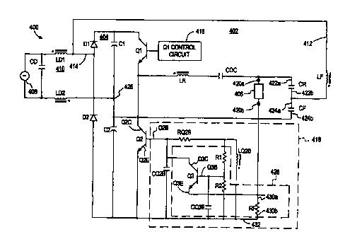
FIG. 8 shows a ballast circuit 400 having an inverter 402 which provides a
feedback signal to a voltage doubling rectifier 404. Current through the lamp
406 is
clamped to a predetermined level and reactive current through a resonant
circuit element
provides the feedback signal to the rectifier 404 for providing linear
operation of the
rectifying diodes D1,D2.
In one embodiment, an AC input signal provided by an AC energy source 408 is
received by a EMI filter 410 formed from inductive elements LD1,LD2 and
capacitor CD.
The filtered AC input signal is rectified by the voltage doubling rectifier
circuit 404 which
is formed from first and second bridge diodes D 1, D2 and capacitors C 1, C2.
A feedback
CA 02321449 2000-08-17
_ WO Q0/38480 PCTNS99/27768
-11-
signal path 412 extends from the inverter 402 to a point 414 between the first
and second
rectifying bridge diodes D1,D2 of the rectifier.
The inverter 402 includes first and second switching elements Q1,Q2 coupled in
a half bridge configuration with a first control circuit 416 controlling a
conduction state
of the first switching element Q 1 and a second control circuit 418
controlling a conduction
state of the second switching element Q2. A resonant inductive element LR has
one
terminal coupled to a point between the first and second switching elements
Q1,Q2 and the
other terminal coupled to a DC-blocking capacitor CDC. A first lamp terminal
420a is
coupled to the DC-blocking capacitor CDC and a second lamp terminal 420b is
coupled
to the second control circuit 418. A resonant capacitor CR has a first
terminal 422a
coupled to the first lamp terminal 420a and a second terminal 422b coupled to
a first
terminal 424a of a feedback capacitor CF. A second terminal 424b of the
feedback
capacitor CF is coupled to a point 426 between the first and second capacitors
C1,C2.
The feedback signal path 412 extends from a point between the resonant
capacitor
CR and the feedback capacitor CF to the point 414 between the first and second
bridge
diodes D1,D2. The feedback signal path 412 includes a feedback inductor LF
which is
inductively coupled with the resonant inductive element LR. The polarity of
the feedback
inductor LF with respect to the resonant inductive element LR is indicated
with
conventional dot notation.
The second control circuit 418 includes an inductive bias element LQ3B for
alternately biasing the second switching element Q2 to conductive and non-
conductive
states and a clamping circuit 428 for limiting the lamp current to a
predetermined level.
The inductive bias element LQ3B, a resistor RQ2B, and a capacitor CQ2B combine
to
control the conduction state of the second switching element Q2 to facilitate
resonant
operation of the inverter. More particularly, the bias element LQ3B, which is
inductively
coupled to the resonant inductive element LR, alternately biases the second
switching
element Q2 to conductive and non-conductive states based on the direction of
the current
through the resonant inductive element LR. The use of an inductive bias
element that is
inductively coupled to a resonant inductive element is well known to one of
ordinary skill
in the art.
The clamping circuit 428 includes a feedback resistor RF having a first
terminal
430a coupled to the lamp 406 and a second terminal 430b coupled to a negative
rail 432
CA 02321449 2000-08-17
WO 00!38480 PCT/US99/27768
-12-
of the inverter. A third switching element Q3, shown as a transistor, has a
collector
terminal Q3C coupled to the base terminal Q2B of the second switching element
Q2, a base
terminal Q3B coupled to the negative rail 432 via a capacitor CQ3B, and an
emitter
terminal Q3E coupled to a point between the feedback resistor RF and the Iamp
406. A
first resistor R1 is coupled between the base terminal Q3B of the third
switching element
Q3 and the inductive feedback element LQ2B and a second resistor R2 is coupled
between
the base terminal Q3B of the third switching element Q3 and the negative rail
432 of the
inverter.
In operation, current through the resonant inductive element LR splits between
the
1o lamp 406 (lamp current) and tire capacitors CR,CF (reactive current). A
series resonance
develops between the feedback inductive element LF and feedback capacitor CF
so as to
generate relatively high voltages across these elements. Since the voltages
are out of phase
with respect to each other, the voltages across the feedback capacitor CF and
the inductive
feedback element LF combine to provide a feedback signal which produces linear
operation
of the rectifier bridge diodes D1,D2.
The lamp current flows from the negative rail 432 through the feedback
resistor
RF. When the current level through the feedback resistor RF becomes greater
than a
predetermined level, the third switching element Q3 is biased to a conductive
state which
causes the second switching element Q2 to transition to a non-conductive
state. More
2o particularly, the current flowing from the negative rail 432 to the lamp
406 generates a
voltage drop across the feedback resistor RF that negatively biases the
emitter terminal
Q3E of Q3. When the negative bias is sufficient to overcome the base to
emitter voltage
of Q3 (about 0.7 volts), the transistor Q3 becomes conductive. The lamp
current is
thereby clamped to a predetermined level.
By providing separate paths for the reactive current and the lamp current, the
lamp
current can be isolated for limiting the lamp current to a predetermined level
without
inaccuracies associated with the reactive current signal. And the reactive
current is
provided to the rectifying diodes for achieving substantially linear operation
of the diodes.
It is understood that the lamp current can be isolated and that the reactive
current
3o can be coupled to the rectifier in other circuit topologies as well, such
as full bridge
inverter configurations and single switching element inverters, like that
shown in co-
pending and commonly assigned U.S. Patent Application No. 09/146,859, filed on
September 3, 1998.
CA 02321449 2000-08-17
- WO 40/38480 PCT/US99l27768
-13-
One skilled in the art will appreciate fiuther features and advantages of the
invention based on the above-described embodiments. Accordingly, the invention
is not
to be limited by what has been particularly shown and described, except as
indicated by
the appended claims. All publications and references cited herein are
expressly
incorporated herein by reference in their entirety.
What is claimed is: