Language selection

Search

Patent 2321473 Summary

Third-party information liability

Some of the information on this Web page has been provided by external sources. The Government of Canada is not responsible for the accuracy, reliability or currency of the information supplied by external sources. Users wishing to rely upon this information should consult directly with the source of the information. Content provided by external sources is not subject to official languages, privacy and accessibility requirements.

Claims and Abstract availability

Any discrepancies in the text and image of the Claims and Abstract are due to differing posting times. Text of the Claims and Abstract are posted:

  • At the time the application is open to public inspection;
  • At the time of issue of the patent (grant).
(12) Patent Application: (11) CA 2321473
(54) English Title: PROCESS FOR MANUFACTURING AN ELECTRONIC COMPONENT, IN PARTICULAR A SURFACE-WAVE COMPONENT WORKING WITH ACOUSTIC SURFACE WAVES
(54) French Title: PROCEDE DE PRODUCTION D'UN COMPOSANT ELECTRONIQUE, EN PARTICULIER D'UN COMPOSANT A ONDES DE SURFACE FONCTIONNANT AVEC DES ONDES DE SURFACE ACOUSTIQUES
Status: Dead
Bibliographic Data
(51) International Patent Classification (IPC):
  • H03H 9/05 (2006.01)
  • H01L 23/552 (2006.01)
  • H03H 3/08 (2006.01)
  • H03H 9/10 (2006.01)
  • H03H 9/25 (2006.01)
(72) Inventors :
  • STELZL, ALOIS (Germany)
  • KRUGER, HANS (Germany)
  • DEMMER, PETER (Germany)
(73) Owners :
  • EPCOS AG (Germany)
(71) Applicants :
  • EPCOS AG (Germany)
(74) Agent: FETHERSTONHAUGH & CO.
(74) Associate agent:
(45) Issued:
(86) PCT Filing Date: 1999-02-05
(87) Open to Public Inspection: 1999-08-26
Availability of licence: N/A
(25) Language of filing: English

Patent Cooperation Treaty (PCT): Yes
(86) PCT Filing Number: PCT/DE1999/000307
(87) International Publication Number: WO1999/043084
(85) National Entry: 2000-08-17

(30) Application Priority Data:
Application No. Country/Territory Date
198 06 818.2 Germany 1998-02-18

Abstracts

English Abstract


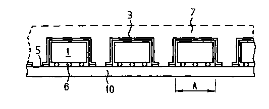
In a process for manufacturing a surface-wave filter, a carrier plate 10 which
can be subdivided into base plates 2 is provided with printed circuits in each
base plate zone A and these are contacted with the active structures of
surface-wave chips 1 by a flip-chip technique. A metal or plastic foil 3 or 4
is then laid on the carrier plate 10 fitted with chips and then processed
under heat and pressure, for example, so that each chip 1 - except for the
chip surface facing the carrier plate 10 - is enveloped and hermetically
sealed on the carrier plate surface in the zones between the chips.


French Abstract

L'invention concerne un procédé de production d'un filtre à ondes de surface, selon lequel une plaque de support (10) pouvant être divisée en plaques de base (2) est pourvue dans chaque zone de plaque de base (A) de pistes conductrices qui sont mises en contact, selon la technique de la connexion par billes, avec les structures actives de puces à ondes de surface, un film de métal ou de matière plastique (3 ou 4) étant ensuite appliqué sur la plaque de support (10) équipée de puces et, par exemple, traité à la vapeur ou thermiquement de telle sorte qu'il enveloppe chaque puce (1), exceptée la surface de puce tournée vers la plaque de support (10), et qu'il repose, dans les zones comprises entre les puces, de façon hermétique sur la surface de la plaque de support.

Claims

Note: Claims are shown in the official language in which they were submitted.


4
Claims

1. Method for manufacturing an electronic component, whereby
a carrier plate (10) that can be separated into base plates (2) is
respectively provided
with interconnects in the base plate regions (A);
one chip (1) per base plate region (A) is contacted to the interconnects
thereof in
flip-chip technique;
a cover film is applied onto the chip-equipped carrier plate (10);
a plastic film (4) composed of an adhesive material in the B-condition is
employed as
cover film;
the cover film is pressure and heat treated such that it envelopes each chip
(1) except
for the chip surface facing toward the carrier plate (10) and lies on the
carrier plate
surface in regions between the chips (1); and
the carrier plate (10) is separated into the individual components (1, 2).
2. Method according to claim 1, whereby the cover film (4) is metal-coated.
3. Method according to claim 1 or 2, whereby the cover film (4) is
adhesive-coated on its surface facing toward the carrier plate (10).
4. Method according to one of the claims 1 through 3, whereby the cover film
is deep-drawn cap-shaped in advance in a grid dimensions defined by the base
plates
(2), is inverted over the chip-equipped carrier plate (10) and has its regions
lying on
the carrier plate (10) joined to the carrier plate (10).
5. Method according to one of the claims 1 through 4, whereby the cover film
is applied onto the chips (1) and the carrier plate (10) by pressure and heat
treatment.
6. Method according to claim 5, characterized in that the pressure and heat
treatment ensues under vacuum.
7. Method according to one of the claims 1 through 6, whereby a ceramic or
plastic plate is employed as carrier plate (10).
8. Method according to claim 7, whereby a through-contacted ceramic or
plastic plate coated with interconnects on both sides is employed as carrier
plate (10).


5

9. Method according to one of the claims 1 through 8, whereby, after
enveloping the chips (1), the cover film is pressed or cast out with plastic
(7).
10. Method according to one of the claims 1 through 9, whereby partial layer
sequences composed of damping compound are applied onto the outside and/or
inside
surface of the metal foil and plastic film (3; 4), these partial layer
sequences being
adapted such that they attenuate disturbing acoustic volume waves, potentially
in
collaboration with a pressing or casting compound (7).
11. Method according to claim 10, whereby filled epoxy resin is employed as
damping compound.
12. Method according to claim 11, whereby epoxy resin filled with SiO2, W,
WO3 or Ag is employed.

Description

Note: Descriptions are shown in the official language in which they were submitted.


CA 02321473 2000-08-17
1
PROCESS FOR MANUFACTURING AN ELECTRONIC COMPONENT, IN
PARTICULAR A SURFACE-WAVE COMPONENT WORKING WITH
ACOUSTIC SURFACE WAVES
The invention is directed to a method for manufacturing an electronic
component, particularly an SAW component working with surface acoustic waves,
comprising a chip with piezoelectric substrate and active filter structures
that are
contacted to interconnects of a base plate, and comprising a cap-shaped
housing that
envelopes the chip and is tightly seated on the base plate.
For protection against disturbing environmental influences, particularly
against chemically aggressive substances and moisture, a potentially mufti-
layer,
usually 2-layer, structured protective films, called PROTEC by the assignee,
is
arranged between base plate and chip given active filter structures contacted
to the
ceramic or plastic base plate in flip-chip technique, i.e. with bumps or,
respectively,
solder balls. Protected by this film, the SAW filter can have casting
compound, for
example epoxy resin, filled under it and cast around it after the flip-chip
bonding
without the active filter structure being thereby coated and the surface waves
being
undesirably attenuated.
Given SAW filters of the ultra-frequency pass range that are contacted in
flip-chip technique, i.e. typically given chip dimensions less than
approximately 2 x 2
2 0 mmz, it has been shown that an adequate stability given alternating
temperature
stressing is established even when the corresponding spaces between base plate
and
chip are not filled.
Deriving from this perception, the object of the invention is to specify a
method that enables the expensive PROTEC encapsulation of the SAW components
to
2 5 be foregone and that nonetheless produces excellent SAW components.
For achieving this object in a method of the species initially cited, the
invention provides that a carrier plate that can be separated into base plates
is
respectively provided with interconnects in the base plate regions, that one
chip per
base plate region is contacted to the interconnects thereof in flip-chip
technique, that a


CA 02321473 2000-08-17
2
cover film, particularly a metal foil or a potentially metal-coated plastic
film, is applied
onto the chip-equipped carrier plate, that the cover film is treated, for
example heat
and pressure treated, such that it envelopes each chip -- except for the chip
surface
facing toward the carrier plate -- and lies tightly on the carrier plate
surface in regions
between the chips, and that the carrier plate is separated into the individual
SAW
components.
Developments of the invention can be derived from the subclaims and the
drawing together with the description thereof. Shown are:
Figure 1 a plan view onto an inventively employed carrier plate in a partially
broken
illustration;
Figure 2 a partially cut and broken side vie« of a first exemplary embodiment
of a
chip-equipped carrier plate according to the method of the invention; and
Figure 3 a second exemplary embodiment of an SAW filter fabricated according
to
the method of the invention, likewise in a partially cut side view.
In the first-cited method, a carrier plate 10, for example a ceramic or
plastic plate, that can be separated into base plates 2 (see Figure 3) along
the parting
lines B-B' and C-C' is provided with interconnects (not shown in the drawing)
in the
respective base plate regions A, these interconnects being usually through
connected to
the backside base plate region. The carrier plate 10 is thereby coated with a
solderable
2 0 metal grid 5 corresponding to the base plate dimensions -- preferably
simultaneously
with the application of the interconnects --, and one chip I per base plate
region is
subsequently ;,ontacted by bumps to the interconnects thereof in flip-chip
technique.
Finally, a cover film -- namely a metal foil 3 having suitable thickness and
ductility -- is applied onto the chip-equipped carrier plate 10 and is
pressure and heat
2 5 treated such, for example in an autoclave or under vacuum, that it tightly
envelopes
each chip 1 -- except for the chip surface neighboring the carrier plate 10 --
, lies on the
metal grid 9 in the regions between the chips 1 and is soldered thereto along
the
solderable metal frame.
As a result of this type of processing the metal foil 3, also be ultrasound
3 0 application along the metal grid 5 as well, the metal foil 3 conforms to
each chip 1


CA 02321473 2000-08-17
3
quasi as cap-shaped housing that has its face edges seated hermetically tight
on the
metal frame 5 or, respectively, on the carrier plate 10.
Assuming no hermetically tight closure is required between foil and base
plate, then a plastic film 4 (see Figure 3) that is potentially metal-coated
for
electromagnetic shielding can be employed instead of the metal foil 3, said
plastic film
being composed, for example, of an adhesive material in the B-condition or
being
adhesive-coated on its surface facing toward the carrier plate 10. This film,
which can
also be subjected to a pressure and heat treatment in an autoclave, also
surrounds the
chip hermetically tight. However, since a metal grid 5 is superfluous given
plastic
films, the face edge 4a of each "plastic housing" is seated directly on the
carrier plate
10 or, respectively, on the base plate 2.
It also proves suitable to deep-draw the metal or plastic foil or film 3 or,
respectively, 4 cap-shaped in a grid dimension defined by the base plates 2
and to
invert this partly deep-drawn foil over the chip-equipped carrier plate 10,
after which it
has its regions 3a or, respectively, 4a lying on the carrier plate 10 tightly
joined to the
carrier plate in the aforementioned way. This possibility is of great
significance
particularly for shrink-free or low-shrink carrier plates.
The housing [sic] that have arisen in this way in copy technique can be
further-stabilized and additionally sealed hermetically tight to a metal
cladding by
2 0 pressing or casting, for example with epoxy resin, as indicated with
broken lines in
Figure 2 (see region 7).
Further, partial layer sequences composed of damping compound can be
applied onto the outside and/or inside surface of the metal foil and plastic
film 3 or,
respectively, 4, these partial layer sequences being adapted such that they
attenuate
2 5 disturbing acoustic volume waves, potentially in collaboration with a
pressing or
casting compound 7.
Filled epoxy resins are especially suited as damping compound, for
example with Si02, W, W03 or Ag as filling constituent.

Representative Drawing
A single figure which represents the drawing illustrating the invention.
Administrative Status

For a clearer understanding of the status of the application/patent presented on this page, the site Disclaimer , as well as the definitions for Patent , Administrative Status , Maintenance Fee  and Payment History  should be consulted.

Administrative Status

Title Date
Forecasted Issue Date Unavailable
(86) PCT Filing Date 1999-02-05
(87) PCT Publication Date 1999-08-26
(85) National Entry 2000-08-17
Dead Application 2004-02-05

Abandonment History

Abandonment Date Reason Reinstatement Date
2003-02-05 FAILURE TO PAY APPLICATION MAINTENANCE FEE

Payment History

Fee Type Anniversary Year Due Date Amount Paid Paid Date
Application Fee $300.00 2000-08-17
Registration of a document - section 124 $100.00 2000-11-27
Maintenance Fee - Application - New Act 2 2001-02-05 $100.00 2001-01-19
Maintenance Fee - Application - New Act 3 2002-02-05 $100.00 2002-01-21
Owners on Record

Note: Records showing the ownership history in alphabetical order.

Current Owners on Record
EPCOS AG
Past Owners on Record
DEMMER, PETER
KRUGER, HANS
STELZL, ALOIS
Past Owners that do not appear in the "Owners on Record" listing will appear in other documentation within the application.
Documents

To view selected files, please enter reCAPTCHA code :


To view images, click a link in the Document Description column. To download the documents, select one or more checkboxes in the first column and then click the "Download Selected in PDF format (Zip Archive)" or the "Download Selected as Single PDF" button.

List of published and non-published patent-specific documents on the CPD .

If you have any difficulty accessing content, you can call the Client Service Centre at 1-866-997-1936 or send them an e-mail at CIPO Client Service Centre.


Document
Description 
Date
(yyyy-mm-dd) 
Number of pages   Size of Image (KB) 
Representative Drawing 2000-11-27 1 6
Cover Page 2000-11-27 1 50
Abstract 2000-08-17 1 60
Description 2000-08-17 3 154
Claims 2000-08-17 2 63
Drawings 2000-08-17 1 17
Correspondence 2000-11-08 1 2
Assignment 2000-08-17 3 91
PCT 2000-08-17 20 800
Assignment 2000-11-27 3 97
Fees 2001-01-19 1 39