Note: Descriptions are shown in the official language in which they were submitted.
CA 02321725 2000-08-24
WO 99/45343 PCT/GB99/00604
ITEM DETECTION/INSPECTION ARRANGEMENT
This invention relates to an arrangement for detecting/inspecting items
prior to them being packaged, and has particular application to
pharmaceutical items, such as tablets, pills, capsules and the like.
Item inspection arrangements, for example for inspecting tablets to
establish if they are whole or broken to some degree, are known which
utilise the passage of the tablets between two plates of a single capacitor.
This results in a change of capacitance and a corresponding signal which
is processed to provide an indication of the result of each inspection.
It has however been established that an item 1 having a rectangular plan,
when disposed between parallel capacitor plates 2, 3, produces a varying
increase in capacitance as it is rotated about a vertical axis (Figure 1).
Since the orientation of the item in space is random, there is a large error
resulting from orientation. A secondary further effect disrupting the
inspection is the 'end' effect, which reduces field density at the mid-point
between the capacitor plates, compared to that nearer each plate.
Accordingly the sensitivity to an item varies as the item is moved along a
line perpendicular to the plates.
An object is to minimise or obviate these disadvantages by providing an
improved detection/inspection arrangement.
An item detection/inspection arrangement of the invention comprises at
least four capacitor plates arranged together in at least two pairs of
opposing or generally opposing plates to provide, in use, at least two
CA 02321725 2003-12-22
WO 99/45343 PCT7GB~9/OOf
-2-
intersecting electric fields, items passing through said fields, in use,
producing respective signalsJpulses dependent on the changes of
capacitance for the pairs of plates, and processing means for producing
from said signalsJpulses, detectionrnspection data for said items.
As used herein, the reference to electrical) fields 'intersecting' includes
actual intersection i.e. by two or more fields which are together
simultaneously in existence, and also spacial intersection, i.e. where the
fields do not exist together at any time but, when they exist separately, are
positioned in space (within the transducer) so that they would intersect if
they did exist simultaneously. Accordingly it will be appreciated that the
invention relates not only to the spacial intersections of the second
embodiment described, where the plates are sequentially pulsed, but also
to actual intersecting electrical) fields as is the case with the first
embodiment where the two pairs of plates are driven not in phase.
According to an aspect of the present invention there is provided an item
detection/inspection arrangement comprising at least four capacitor plates
arranged together in at least two pairs of opposing or generally opposing
plates,
forming at least two capacitive cells, to provide, in use, at least two
intersecting
electric fields, items passing through the fields, in use, producing
respective
signals/pulses dependent on the changes of capacitance for the pairs of
plates,
and processing means for producing from the signals/pulses,
detection/inspection data for the items, wherein one plate of each pair is a
sense
plate having a voltage induced thereat by the driving, in use, of drive plate
means
formed by at least the opposing or generally opposing plate of the pair,
wherein
the drive plate means comprises at least one further capacitor plate, the
CA 02321725 2003-12-22
2a
opposing or generally opposing plate and the further plate being on,
respective
sides of a transducer providing the intersecting electric fields, in use, the
further
plate being on a side of the transducer at an angle of 90° or greater
to respective
sides of the transducer on which are the sense plate and the opposing or
generally opposing plate, and wherein the capacitor plates are formed from
electrically conducting material on the inner surface of an insulating layer,
which
layer has its outer surface formed with electrically conducting material, the
electrically conducting material of the outer surface, in use, being at a
voltage
which provides a screen to shield a sensing area of the transducer from items
outside the area.
According to another aspect of the present invention there is provided, an
item
detection/inspection arrangement comprising at least four capacitor plates
arranged together in at least two pairs of opposing or generally opposing
plates
provide, in use, at least two intersecting electric fields, items passing
through the
fields, in use, producing respective signals/pulses dependant on the changes
of
capacitance for the pair of plates, and processing means for producing from
the
signals/pulses, detectionrnspection data for the items, wherein one plate of
each
pair is a sense plate having a voltage induced thereat by the driving, in use,
of
drive plate means formed by at least the opposing or generally opposing plate
of
the pair, wherein respective signal processing circuits are coupled to
respective
output signals from the sense plates, each processing circuit including an
amplifier which produces an output, in use, which is proportional to the
voltage
induced in the sense plate by the capacitance between the sense plate and the
drive plate means, and wherein the output from the amplifier, in use, is
coupled
via a capacitor to a first switch which opens and closes so as to effect
charging
of the capacitor.
CA 02321725 2003-12-22
2b
The invention will now be described, by way of example, with reference
to the accompanying drawings, in which:
Figure 1 is a schematic plan view showing rotation of an item about a
vertical axis between two capacitor plates,
Figure 2 is a schematic plan view of part of a detectionrnspection
arrangement of the invention,
Figure 3 is a side view of the Figure 2 arrangement,
CA 02321725 2000-08-24
WO 99/45343 PCT/GB99/00604
-3-
Figure 4 is a diagram schematically showing the effective electrical
network of the Figure 3 arrangement,
Figure 5 is a circuit diagram of an arrangement of the invention,
Figures 6 and 7 schematically show two side views respectively at
90°
apart of an item rotated about a horizontal axis between a pair of
capacitor plates in an arrangement of the invention,
Figure 8 is a view like Figure 6, illustrating an item falling in two
alternative orientations between the plates with its longest dimension in
the horizontal and the vertical respectively,
Figure 9 shows the D.C. output pulses for the two respective
configurations of fall shown in Figure 8,
Figure 10 is a perspective view of part of a transducer of a
detection/inspection arrangement according to a second embodiment of
the invention,
Figure 11 is a similar view to Figure 3, showing the complete transducer,
Figure 12 is a perspective view of the transducer in use,
Figure 13 is a perspective view like Figure 10 showing part of a transducer
according to another embodiment,
CA 02321725 2000-08-24
WO 99/45343 PCT/GB99/00604
-4-
Figure 14 schematically shows an arrangement of pulse means for driving
the transducers of Figures 11 or 13,
Figure 15 shows a conditioning circuit with an associated timing circuit
for producing said pulse means,
Figure 16 shows schematically the relative timing of events for one set of
capacitor plates for the transducer of Figure 11 or Figure 13, and
Figure 17 is a block diagram of an arrangement of discriminating devices
for processing signals from the processing circuit of Figure 15.
The present invention provides a capacitative arrangement (hereinafter
referred to as a transducer) for detecting/inspecting items in which the
transducer's susceptibility to orientation of the item being measured is
reduced. Figures 2 and 3 show one possible embodiment. In plan view
there are four capacitor plates, each having an inner electrode 10 and an
outer electrode 11. Each outer electrode is driven with a sine wave of the
same frequency, but with a different phase, each being 90° shifted from
the adjacent plate, as indicated. There are therefore two co-existent
capacitors at right-angles to each other, providing respective electrical
fields which intersect. However because their drive voltages and
detection circuits are 90° out of phase they have practically no effect
on
each other. Figure 4 shows the effective electrical network provided by
the two capacitor arrangement.
Figure 5 shows a block diagram of one embodiment of an excitation and
detection circuit for one pair of plates (e.g. the 0/180° pair). The
circuit of
CA 02321725 2000-08-24
Wo 99/45343 PCT/GB99/00604
-5-
the adjacent pair is substantially the same. It shares the same oscillator
but uses the 90° and 270° signals, instead of 0° and
180°, where
appropriate.
A stabilised oscillator 12 produces a sine wave at around 10 kHz. It has a
0° output and an 180° phase output. It also produces a 0°
reference
square wave with the same phase as the 0° sine wave. The 0° and
180°
sine waves feed the outer electrodes 11 of the plates.
The inner electrodes 10 and the outer electrodes 11 form three series
capacitors. The effect of an object/item 13 passing between the inner
electrodes is slightly to reduce the voltage difference existing between
them, i.e. the voltage across the centre capacitor. This change is small
because of the relatively small initial capacitance and the much larger
capacitance between inner and outer electrodes. In practice the inner and
outer electrodes may be formed by areas of copper track on the two sides
of electrically insulating means, for example a fibre-glass printed circuit.
The signal on each inner electrode 10 is at very high impedance and is
immediately buffered by preamplifiers 14 which are mounted physically
near to those electrodes. Their low impedance outputs are then fed to a
differencing circuit 15 which produces an output signal resembling the
difference in voltage between the inner electrodes. A following pulling
device 1 b subtracts most of the large standing signal which is present
when no item is being measured. In practice the pulling circuit operates
automatically by varying the amount of 0° or 180° sine wave
which is
added to the signal in order to produce a near zero output with no item
present between the plates. Although not shown on the diagram it also
CA 02321725 2000-08-24
WO 99/45343 PCT/GB99/00604
-6-
subtracts any residual signal which is induced from the adjacent places by
using a second synchronous detector which uses the 90° square wave as
its timing reference.
The output of the nulling circuit 16 passes through a main amplifier 17 to
a synchronous detector 18. This produces a D.C. output which is
proportional only to the in-phase signal. Any 90° signal is inherently
ignored by it. The resulting D.C. output is largely proportional to the
increase in capacitance caused by the item passing through the
corresponding plates and largely unaffected by the adjacent plates. It is
then passed to the subsequent device for analysis, possibly by way of a
low-pass filter 19. There is a corresponding D.C. output from the circuit
of the adjacent plates. In simple terms the subsequent device simply adds
the two D.C. outputs together to produce a D.C. signal which is largely
immune to rotation about the vertical axis.
When considering the horizontal axes, reference is made to Figures 6 and
7 which shows two sides of a simple pair of plates and the rectangular
object 13 being rotated about the two horizontal axes respectively. It can
be seen by observation that the rotation in Figure 7 will have no effect
because of the symmetry of the plates about that axis. However the
rotation in Figure 6 is the same as that shown about the vertical axis.
When visualising a second pair of plates being added to the arrangements
of Figures 6 and 7, it can be seen that a rotation about each horizontal axis
will produce nil effect in one pair and a finite effect in the other,
depending on which horizontal rotational axis is being considered. A
tablet or similar object which is falling with its longest dimension in the
horizontal produces a higher and longer D.C. output pulse 20 than one 21
CA 02321725 2000-08-24
WO 99/45343 PCT/GB99/00604
_7_
falling with its longest dimension in the vertical, as shown in Figures 8
and 9. The voltage is higher because of the rotation effect. The poise is
longer because the item spends more of is travel with its entirety between
plates.
The two D.C. output signals/pulses are therefore capable of providing
sufficient data in their pulse length and height to enable a subsequent
processing device to discern the amount of material in an item largely
irrespective of its orientation between the pairs of plates.
The two D.C. outputs are intended to be fed to respective Analogue to
Digital converters which are both read by a microprocessor. The
microprocessor will be programmed to memorise the combination of D.C.
levels and pulse lengths which correspond to the different orientations of
the same (perfect) item falling through the plates. For example a large
batch (say 1000) known, perfect items will be fed through the plates
sequentially and the magnitudes and pulse lengths of the two D.C. signals
memorised for each item. When the unknown items are subsequently fed
through the device the processor will compare the resulting D.C. levels
and pulse lengths with the known ones for the perfect items, to determine
if the item is recognised as being acceptable in volume.
None of the plates are connected to ground (zero volts) potential. This is
to preserve symmetry and to equalise the effects of stray capacitance to
the metal mass which in practice will surround the whole device. It is
envisaged that a simpler device could be produced where one plate of
each pair could be grounded, although it may produce inferior results.
CA 02321725 2000-08-24
WO 99/45343 PCT/GB99/00604
-8-
The aforementioned problem of varying field density is largely solved by
the respective outer electrodes being substantially larger than the inner
ones. The bulge in the field occurs mainly at the edge of the outer
electrodes instead of the inner ones. This is because the voltage across
the inner electrodes is almost the same as that across the outer ones. The
effect is therefore (roughly) reduced by the ratio of heights of the inner
electrodes to the outer electrodes. The presence of the adjacent plate also
serves to 'contain' the field from bulging.
The arrangement and driving of the outer plates 11 is such that each pair
forms a screen to shield the inner plates 10 from influences external of the
transducer thus preventing sensing of objects which are outside the
transducer, and preventing cross-talk between adjacent transducers.
Instead of 4 plates, more could be used, preferably in pairs, for example
four pairs may be suitable.
The arrangement is of course applicable to items which are not
rectangular, e.g. circular tablets, tubular capsules or the like.
Whilst the first embodiment described above represents an improved
arrangement in respect of rotation of the measured item about the vertical
axis, the problem of rotation about the longitudinal and lateral axes in the
horizontal plane of the transducer is not satisfactorily solved by
measurement of the length of the pulse, as this can be affected by other
factors, such as the velocity of the item.
CA 02321725 2000-08-24
WO 99/45343 PCT/GB99/00604
_g_
Accordingly the second embodiment of the invention shown in Figures 10
to 17 relates to a further improved detection/inspection arrangement. As
with the transducer described in relation to the first embodiment, the
capacitative arrangement or transducer 22 is in the form of a box with an
open top and an open bottom, having plates on all four sides thereof.
However this embodiment has a different arrangement of plates, as well as
a different method of excitation and of signal processing, and represents
an alternative and improved method of attempting immunity from errors
due to orientation of the object.
Figure 10 shows, for simplicity, the arrangement of one set of plates only.
All the plates are formed in a conducting material on the inner surface of
electrically insulating means, such as a fibre-glass sheet. The outer surface
of the sheet is largely covered with another conducting surface which is
connected to ground, i.e. zero volts with reference to the remainder of the
circuit. The plates on the inner surface can be considered to be
equivalent to an inner electrode, with the outer conducting surface being
equivalent to an outer electrode.
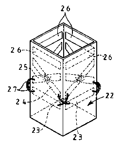
As shown in Figure 10, there is a first plate 23 approximately half way
down one of the sides, and second and third plates 24, 25 respectively on
the respective sides of the transducer adjacent the side on which the plate
23 is disposed, the second and third plates extending upwardly from and
relative to the first plate 23 to terminate just short of the remaining fourth
side of the transducer, at which adjacent the open upper end thereof is
disposed a fourth plate 26. All the plates are, in this embodiment,
generally rectangular, and the second and third plates are electrically
connected to the first plate as shown, these three plates being known as
CA 02321725 2000-08-24
WO 99/45343 PCT/GB99/00604
-10-
drive plates, the fourth plate being known as the sense plate. If required
the plates could be tapered widthwise, i.e. be trapezoidal.
Figure 11 shows the complete transducer which has four of the sets of
plates shown in Figure 2 around its four surfaces respectively. With this
particular embodiment, the 'diagonal' plates on each face would pass
through each other, and this would prevent them from having separate
voltages. Thus each of the plates 24, 25 is divided at its centre, with there
being connecting wires 27 as shown between the halves of each plate.
The arrangement in this embodiment thus produces four electrical fields
which each slope at an angle to the horizontal, which angle is typically in
the range 30° to 60°, and at the centre of the transducer,
spacially
intersect, i.e. they would actually intersect if produced at the same time
rather than being produced by the drive plates being driven sequentially.
With an angle in this embodiment of 45 °, when an item to be
measured
rotates in space, it can never be more than 45° from the axis of any of
the
fields. In simple terms, the space at the centre of the transducer, where
the four fields spacially intersect, now has much more effect than with the
arrangement of the first embodiment, because the item is sensed four
times, sequentially. When the resulting signals are added together, an
item which is located at the centre can have up to four times the effect as
one which only intersects one field. Accordingly a weakness of the first
embodiment has been attended to. This centre sensitivity can then be
increased or reduced more to equal that at other points, by adjusting
dimensions of the plates, segmentation of the plates and voltages on the
segments.
CA 02321725 2000-08-24
WO 99/45343 PCT/GB99/00604
_t1_
Since the sense plate 26 has a voltage which is very near to zero, and zero
volts is also on the outer surface of the transducer, there is, to a large
extent, only a voltage gradient in the space which is directly between the
plates of each set. This brings some improvement over the earlier
arrangement in which the field tended to bulge more in the vertical axis.
As with the first embodiment, it is important that sensing only occurs
within the area bounded by the plates. On a typical counting/grading
machine there could be up to 20 such transducers mounted immediately
against each other, in a line. It is therefore vital that the items falling
through one transducer are ignored by any transducer which is adjacent to
it. The transducers are therefore not simple capacitor plates which would
inherently sense the space bounded by them and to a degree the space
outside, due to fringing. The equivalent electrical circuit is therefore not a
simple pair of plates for each axis but a multiplate network in which the
outer electrodes are joined either to ground or a low impedance generator
(voltage source) which has the same effect as a ground shield in
containing the sensing area. Cross-talk between adjacent transducers is
also prevented by this arrangement.
Although not described with the first embodiment, Figure 12 shows how,
in use, an item to be inspected/detected by a capacitative arrangement of
both embodiments wilt pass through a guide, for example a polymer tube
28. Environment and pharmaceutical industry practices nowadays insist
that there is some material between the transducer plates and the falling
item. If the items are likely to come into contact with the insulating guide,
the inspection/detection method would suffer from a build-up of static
electricity on the surface of the insulating guide, which is required to be a
good insulator in view of the sensing method. If it was slightly
CA 02321725 2000-08-24
WO 99/45343 PCT/GB99/00604
-12-
conductive, it would distort the electric field which is set up by the plates,
to an extent which would destroy its measuring capability. The items
passing through the tube will inevitably contact the inside thereof, and in
doing so cause a build-up of free electrons on the inner surface, with the
result that an electrostatic field is therefore formed. Subsequent items,
also having free electrons at their surface, cause this field to be
momentarily changed as they fail through it, and a resulting, interfering
signal would be produced. The magnitude and form of that signal can be
such that unwanted outputs can occur in most signal processing methods.
Any insulating coating which is applied directly to the transducer's plates
could suffer from the same problem with a build-up of static electricity.
As will be described hereinafter, this problem is solved by the
arrangement of the second embodiment.
As a refinement to the transducer arrangement shown in Figure 11, any
part of the drive plates can be arranged to have different voltages at
different places along their lengths. This can be achieved by forming a
plate from a resistive material, or by cutting it into sections and driving
each section at a different voltage, for example as shown in Figure 13.
The voltage gradient which is so produced can be adjusted to trim the
three-dimensional voltage field for optimum distribution of gradients. It is
envisaged that this arrangement would be under processor control, so that
different voltage patterns may be set-up to optimise the performance for
different shapes of items, particularly pills.
The four sets of drive plates, whether solid as shown in Figure 11, or
having gradient sections as shown in Figure 13, are driven sequentially
with high voltage pulses as shown in Figure 14, one frame, for example,
CA 02321725 2000-08-24
WO 99/45343 PCT/GB99/00604
-13-
taking a little less than 1 millisecond. The waveforms are produced by
(silicon) switches, which connect each plate to a positive high voltage and
then a negative high voltage in turn. The switches are driven from a
timing circuit shown in Figure 15.
A different source voltage could be supplied to drive each plate section.
Alternatively, one or more of the sections could be connected electrically
to the voltage on plate 23 via resistors (or the like), to provide unequal
potential along the sectioned plate with different resistance values.
In the example shown in Figure 13, the whole excitation is applied to the
horizontal drive plate 23 and proportions of it are applied through
resistors to the gradient sections 24a, 24b and 25a, 25b. The could be
any number of gradient sections and, at the limit, the whole drive plate (or
plates) could be formed from a resistive material with its lowest potential
point connected to ground, or a low voltage. In this way it would form
both the electrode and the method of producing the gradient.
Figure 15 shows the signal processing circuit as well as the timing circuit
and Figure 16 shows the relative timing of the events concerning one set
of plates.
The output of each sense plate is fed to a respective amplifier 29, which
has an extremely high input impedance and low input capacitance so as
not unduly to influence the voltage which is induced in the sense plate by
its corresponding drive plate. The output of the amplifier 29 is then fed
via a capacitor 30 to a switch 31. When the amplifier has had time to
respond to the positive excitation voltage, switch 31 closes under the
CA 02321725 2000-08-24
WO 99/45343 PCT/GB99/00604
-14-
influence of signal X from the timing circuit. Capacitor 30 therefore
charges to the corresponding output voltage of amplifier 29. Switch 31
opens after a short time leaving capacitor 30 holding the voltage to which
it was charged and its right-hand end still at zero volts. When the
excitation switches to a negative voltage, the right-hand end of capacitor
30 is driven, by amplifier 29, to a negative level which is equal to the
peak-to-peak transition of the output of amplifier 29. Any quiescent
voltage present at the output of amplifier 29 is not reflected in this
voltage.
This negative voltage is buffered by an amplifier 32 (which also has a very
high input impedance) and fed to a switch 33. Very shortly after the
transition in drive voltage, switch 33 closes for a few microseconds and
transfers the output voltage of buffer amplifier 32 in to a capacitor 34.
This is effectively a sample-hold circuit. The voltage in capacitor 34 is
further buffered by an amplifier 35 so as not to drain it away during the
remainder of the frame. The effect of this is to give a D.C. voltage on the
output of buffer amplifier 35 which is proportional to the voltage induced
in the sense plate by the capacitance between the drive and sense plates.
Any item which comes between the drive and sense plate of that channel
will cause a change in that induced voltage and therefore a corresponding
change in the output voltage of buffer amplifier 4.
The other three channels of the transducer have corresponding elements
and the four D.C. voltages are added together by a summing amplifier 36.
It can therefore be seen that in rotating the item through any axis there
will be a significant reduction in orientation errors as it intercepts the
four
fields.
CA 02321725 2000-08-24
WO 99/45343 PCT/GB99/00604
-15-
The combined analogue output of the summing amplifier at Z is then
(typically) passed to discriminating devices as shown in Figure 16,
comprising:
1) A low-pass filter 37 to remove unwanted high-frequency
fluctuations in the analogue signal.
2) A differentiator 38 or similar circuit to remove the quiescent
voltage and leave only the change in voltage which is caused by the
presence of the item.
3) An optional multiplexor to enable multiple transducers to be
sampled (if required).
4) An Analogue to Digital converter 39.
5) A Computer, microcomputer, microprocessor or Digital
Signal Processor (DSP) 40 to record the way that the changes in the
combined analogue signal change with time and to decide if a
particular item has sufficient material to be classed as an acceptable
item or not, and give digital outputs in response to the amount of
material which is in each item. These digital outputs can be used to
energise actuators to divert defective items out of the main stream.
It can also detect if two or more items have fallen through the
transducer simultaneously and is able to batch acceptable items into
groups having a predetermined quantity.
6) An operator interface 41 to enable monitoring of the signal
produced by each item and to enable setting-up of the parameters
which are associated with accepting, rejecting, counting and
hatching the items.
It is clear that the functions of the devices shown in Figure 16 could be
carried out by other means; indeed most of them by a computer,
CA 02321725 2000-08-24
WO 99/45343 PCT/GB99/00604
-16~
microprocessor, microprocessor DSP. The diagram is only indicative of
the steps that may be taken to process the signal and act upon it. Such
action is the rejection of defective items out of line and counting and
hatching of acceptable items.
A significant feature of this embodiment is the relatively high immunity to
the effects of static electricity previously referred to. It has been
determined by measurement that the signals resulting from this static
electricity can vary at a rate of up to (typically) 2 volts per 100
microseconds (measured at the output of amplifier 2 on Figure 6). The
voltage and rate of change of voltage depend on many factors. This
embodiment has significantly reduced the effect by the arrangement of the
timing of switches 31 and 34 in Figure 6. The only time when the circuit
is receptive to the effects of static electricity is between the opening of
switch 31 after closure and the opening of switch 34 after closure on each
channel (shown as the asensing window" on Figure 16). This arrangement
enables that window to be open for a very short time, typically 5
microseconds. During that time the voltage which is due to static
electricity will have only changed by around 0.1 volts, compared by the
required signal which has an amplitude of several volts.
As with the first embodiment, the transducer could have more than four
sides.
In alternative arrangements:
1) The drive plates could be mounted on the outer surface of the wall
CA 02321725 2000-08-24
WO 99/45343 PCT/GB99/00604
_17_
material of the transducer, with the earth plate on the inside, the surface
having windows in it to allow the field from the drive plates to pass
through. This arrangement has particular practical advantages.
2. The drive plates could be excited with sine waves in a similar
manner to the first embodiment and the signal conditioning could use
phase-sensitive rectifiers.
3. The outputs of the separate buffer amplifiers in Figure 15 could be
fed directly to analogue-digital converters to enable them to be combined
in the software of a computer, microcomputer, microprocessor or DSP.
Whilst described specifically in relation to the two embodiments of the
invention relating to a detection/inspection arrangement with at least two
intersecting electrical fields, the transducer arrangement described in
which the sensing area is shielded/screened from influences external
thereof is itself considered inventive per se and can be utilised in
applications other than those described and illustrated herein.