Note: Descriptions are shown in the official language in which they were submitted.
CA 02322419 2000-09-08
1
OPTICAL SENSOR SYSTEM FOR DETECTING THE POSITION OF AN
OBJECT
The invention relates to an optical sensor system for exploring objects and
for
detecting their position. Preferably, this sensor system can be arranged at
autonomous
mobile systems, so that it is possible for them to orientate themselves in an
unknown
environment.
Autonomous mobile systems, which are in the making and planning, will be found
in
the future more frequently in household environments as well. They will cant'
out
transport and cleaning tasks in that they autonomously carry out the tasks
imposed on
them with the aid of an orientation system, which makes it possible for them
to create
an image of their environment. Apart from the different path planning and
evaluation
algorithms, the sensor system for detecting obstacles in the environment of
the
autonomous mobile unit is extremely important. In order to make autonomous
mobile
systems attractive to consumers, it is particularly important that they can be
produced
in large quantity cost-efficiently and technically simple. Therefore, the
sensor systems
of the autonomous mobile systems must be robust and able to be produced
inexpensively.
The prior art discloses optical sensor systems that carry out the detection of
objects by
means of triangulation. For example, a specific measuring method carnes out an
active triangulation with strip lighting. The main elements of such a
measuring
system are a light source, which illuminates a strip in space, an optical
imaging
2 5 system, a two-dimensional image receiver and an electronic unit for
processing and
evaluating the signals received by the image receiver. For purposes of
performing a
triangulation, such a system requires a light source, which exclusively
illuminates a
space strip. An important feature of this light source is the surface density
of its
emitted luminous power. A great power density for being able to also recognize
dark
3 0 objects are [sic] a requirement to be met by such a light source. Another
feature of
CA 02322419 2000-09-08
2
such light sources is the thickness of the illuminated strip, which thickness
influences
the size of the detectable space area and the resolution during the position
measuring
of detected objects.
The following possibilities for fashioning light sources for the output of
luminous
strips are currently known: a cylindrical lens in front of a collimator
objective, which
collimates the light of a laser source or of a filament, halogen or arc lamp;
the
parallelization of light from a filament or halogen lamp with the aid of an
collimator
objective and its spreading by means of a cone mirror. The utilized imaging
system
must meet two main requirements. On one hand, it must image the space area to
be
measured onto the surface of the two-dimensional image detector; on the other
hand,
it must assure the desired position resolution regarding the objects to be
measured. In
this context, the position resolving capacity is the smallest distance between
objects,
which can still be resolved after the imaging onto the opto-electrical
converter. It is
determined by the utilized converter and also by the imaging system. The task
to
image a large space area, optimally in the form of a whole half space in a
wide-angle
manner and to thereby generate a sufficient distance resolving capacity with
the same
objective, represent [sic] contradictory requirements [sic]. A possible means
for
enlarging the measurable space area by means of such an imaging system is the
2 0 application of a wide-angle objective, which generates an image that is
free of
distortions. However, such objectives with a plurality of lenses have the
disadvantage
that they cannot image the entire half space around the objective. Other
objectives, in
turn, which image an entire half space, no longer work without distortions and
are
expensive to buy. Distorting objectives also influence the position resolution
during
2 5 the triangulation. The distance in the imaging area between the images of
the back-
scattered light of two neighboring objects, which are close to the imaging
system, is
represented larger compared to the two neighboring objects that are situated
further
away from the imaging system. This has the effect that the position resolution
becomes poorer with an increasing distance from the objective or,
respectively,
3 0 imaging system. The imaging system cannot image far-away objects
sufficiently far-
CA 02322419 2000-09-08
3
away from one another by applying normal or aspherical refracting surfaces, as
they
are conventional for normal objectives. In order to image such objects, it
would be
necessary to use an optical imaging element that is optimized for this
specific
purpose; however, said imaging element is not known from the literature.
The European publication EP 0 358 628 A2 with the title "Visual navigation and
obstacle avoidance structured light system" discloses a triangulation system
for
applying to mobile vehicles, which triangulation system uses strip
illumination and a
normal objective in an imaging system. The disadvantages of this solution are
that the
vehicle can only detect obj ects in front, namely obj ects situated in driving
direction
and that only a restricted area or close objects can be utilized with a
sufficient
resolution for the distance measuring of objects due to the utilization of a
normal
objective. The articles of R. A. Jarvis, J. C. Byrne: "An automated guided
vehicle
with map building and path finding capabilities"; in R. C. Bolles and B. Roth,
publisher, 4'~ International Symposium on Robotics Research, p. 497-504, MIT
press, Cambridge, Massachusetts, 1998, - and Y. Yagi, Y. Nishizawa, M.
Yachida:
"Map based navigation of the mobile robot using omnidirectional image sensor
COPIS, Proc. Of the 1992 IEEE International Conference on Robotics and
Automation, Nice, France, May 1992 discloses to carry out the imaging of the
2 0 environment by means of a cone mirror and an objective. The utilized cone
mirror
does not change the resolving capacity of the system with respect to far-away
objects.
Furthermore, it is determined by the camera objective. The article of J. Hong,
X.
Tan, B. Pinette, R. Weiss, E. M. Riseman; "Image-based Homing, Proc. Of the
1991 IEEE International Conference on Robotics and Automation, Sacramento,
2 5 California, April 1991 discloses to carry out the imaging of the
environment by
means of a spherical ball. However, a strip lighting, which could be used for
the
triangulation, is not utilized. Such what are referred to as passive systems
have the
disadvantage that the objects are not illuminated by a light beam with known
height
level, so that position information items are very difficult to obtain, since
a
3 0 triangulation cannot be performed. Realtime image processing systems,
which require
CA 02322419 2000-09-08
4
a great outlay with respect to computer capacity, must be used for the
evaluation.
Furthermore, the article of P. Greguss: "PAL-Optik basierende Instrumente fuer
Raumforschung and Robot-Technik, in Laser and Optoelektronik 28 (5) / 1996,
page
43-49 discloses the utilization of a PAL-objective for the applications of
navigation
tasks with respect to autonomous mobile robots. The PAL-objective of Greguss
is a
wide-angle imaging element, which contains two mirrorin [sic] and one
refracting
aspherical surface and which is able to image an entire half space. The
application of
the PAL-optics as imaging element of an active triangulating obstacle
recognition
system for robots is described there.
Therefore, the invention is based on the object of proposing an optical sensor
system,
which can be attached to mobile vehicles, such as autonomous mobile robots;
which
is fashioned technically simple; which enables a detection of obstacles in all
directions around the vehicle, whereby its imaging system has the position of
objects
in the close range of the system with respect to distances smaller than 50 cm
and also
in the remote range of the system with respect to distances of more than 2 m
an
sufficient position resolving capacity of approximately S-10 cm an angle
resolution of
< 1°. [sic]
2 0 This object is achieved according to the features of patent claim 1.
Developments of
the invention derive from the dependent claims.
Advantageously, the described sensor system is composed of light sources,
which
illuminate the environment of the autonomous mobile unit in the form of strips
around
2 5 the unit, since [sic] so that obstacles or, respectively, objects can be
simultaneously
detected all around the unit. Advantageously, a plurality of light sources
that are
above one another can be provided, which are switched on in different time
intervals,
so that different height dimensions of the space can be detected or,
respectively,
measured. Advantageously, the light that is back-scattered by illuminated
objects is
3 0 implemented [sic] by using a specific wide-angle imaging element, which
only has
CA 02322419 2000-09-08
one single arched, spherical or aspherical, mirroring surface for the light
guidance, in
connection with an objective and a filter, as well as with a photo-electrical
converter,
whereby the imaging system projects the environment onto the converter. This
arrangement makes it possible to solve this task with an optimally low
technical
5 outlay. Advantageously, the best space covering and the best position
resolving
capacity is achieved in a development of the invention in that the shape of
the
aspherical mirroring surface of the wide-angle imaging system is described
with the
aid of spline functions. The spline function describes the shape of the
imaging
element as follows: areas that are further away are represented in a stretched
manner,
depending on the utilized objective, due to the spline function. On the basis
of the
spline function, the distance areas and the sub-areas of the aspherical
imaging element
that are valid for the respective distance areas are described such that the
adjacent
polynomial functions exhibit the same value and the same derivations in the
respective transfer points, so that the utilized function is continuous and
without
fractions. What is advantageously achieved by utilizing such an imaging system
is
that simple objectives with a normal viewing angle can be used for the wide-
angle
linear imaging characteristics that is necessary with respect to a further
development
of the invention. Due to the utilization of spline functions, it can be
achieved that
light, which is back-scattered from areas that are further away, is pre-
distorted before
2 0 it passes through the objective, so that areas that are further away can
be represented
with a higher resolution as it would be normally possible by means of the
objective.
In this way, an imaging system is made available that offers a simple
economical
solution for the manufacture of wide-angle, linear optical systems.
2 5 Exemplary embodiments of the invention are explained in greater detail on
the basis
of images. Shown are:
Figure 1 an exemplary embodiment of a sensor system.
3 0 Figure 2 a possible arrangement of a utilized light source in side view.
CA 02322419 2000-09-08
6
Figure 3 a possible arrangement for generating a light strip around the
sensor system.
Figure 4 a further embodiment for generating a light strip around the sensor
system.
Figure 5 a further embodiment for generating a light strip around the
imaging device.
Figure 6 a possible construction of the sensor system on a vehicle or,
respectively, robot in side view.
Figure 7 a plan view onto the sensor system and a vehicle.
Figure 8 a sensor system for the utilization with an one-dimensional photo-
electrical converter.
Figure 9 an embodiment with two-dimensional optical position detector.
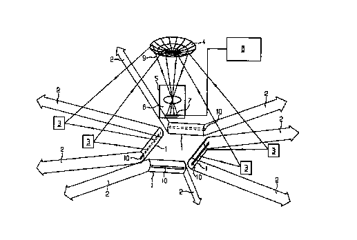
As shown in Figure 1, a possible embodiment of a described sensor system,
which
illuminates a space strip all around, is composed of 4 light sources 1. It is
particularly
important with respect to the arrangement of these light sources for
illuminating a
light strip that these light strips are situated in a plane that is
essentially plane-parallel
2 5 to the base on which the autonomous mobile unit, which has the sensor
attached,
moves. If this plane-parallel arrangement is not possible, the triangulation
is made
more difficult, since it is important, when the reflect [ sic] light beams are
evaluated,
that they have met the reflecting objects under different angle positions, so
that
different triangulation angles result for the triangulation for determining
the distance
3 0 of the objects. The light sources 1 thereby generate light strips 2, which
illuminate the
CA 02322419 2000-09-08
7
space. The utilized imaging element 4 projects the light that is back-
scattered from
the objects 3 through the objective 6 onto the photo-electrical converter 7,
which, in
this arrangement, is fashioned as a two-dimensional CCD image detector of a
camera
5. The photo-electrical converter 7 is in connection with an evaluation
electronic unit
8, which is at, for example, is in a computer [sic], which evaluation
electronic unit 8
determines the position of objects 3, due to the image projected onto the
photo-
electrical converter 7, upon employment of the principle of the active optical
triangulation, whereby particularly the imaging properties of the objective 6
and of the
imaging element 4 are utilized in connection with the level of the plane in
which the
light strip is illuminated. Advantageously, the sensor system is utilized on
mobile
vehicles 12, such as a mobile robot. The current information items thereby can
be
determined by means of the evaluation electronic unit 8 via the control of the
vehicle
12 or, respectively, of the robot, and the further driving path of the unit
can be
planned as a result of these information items. These information items
indicate the
positions of objects 3, for example, under which the vehicle 12 moves through,
or
between which the vehicle 12 must move.
In the embodiment shown in Figure 1, the optical axis of the imaging element 4
is
2 0 advantageously perpendicularly directed toward the light strip 2, which
are [ sic]
outputted by the light sources 1. In this embodiment, the imaging element 4 is
fashioned as an optical element having a spherical or aspherical mirroring
surface 9,
whereby the outside of the mirroring surface 9 is used for the imaging of the
reflected
light beams in the imaging system. The light strips outputted by the light
sources and
2 5 the light beams reflected by the objects 3 are thrown via the imaging
element 4
through the objective 3 onto the light detector 7, as it is schematically
shown by
means of the beam paths, which are provided with numbers. The distance of the
light
beams impinging onto the photo-detector 7 is characterizing for the distance
of the
objects 3 from the sensor system depending on the imaging properties of the
objective
3 0 and the imaging element 4. In the embodiment of the sensor system shown in
Figure
CA 02322419 2000-09-08
8
1, any arbitrary two-dimensional image detector 7 can be used. For example, a
photodiode matrix can be applied as a photo-electrical converter 7 instead of
a two-
dimensional CCD sensor.
In side view, Figure 2 shows a possible basic embodiment of the applied light
source
1. The light source 1 shown in Figure 2 is composed of a cylindrical minor 11,
which
expediently exhibits an aspherical cross-section and is composed of light
emitters 10,
which can be light-emitting diodes, for example. These light emitters are
situated in
the focus line of the cylindrical mirror 11. The light emitters 10, following
one
another, are arranged in series [sic] in the focus line of the aspherical
cylindrical
mirror 11, so that the light-emitting surfaces of the light emitters 10 point
in the
direction of the aspherical cylindrical mirror 11. The light emitted by the
light
emitters 10 thereby initially reaches the aspherical cylindrical mirror 11 and
subsequently emerges as a light strip 2 projected by the mirror. As a result
of the
utilization of an aspherical mirror shape that is adapted to the light
emitters 10, the
light source 1 illuminates a parallelized light strip. It must be mentioned in
this
context that light-emitting diodes (LED) represent a cost-efficient, simple
and small
light source and that an inexpensive light source can be made available by the
selected
arrangement of the light-emitting diodes on the axis of the cylindrical
mirror.
As shown in Figure 3, one possible basis arrangement for generating a light
strip 2 is
composed of a part of a cylindrical mirror. The cylindrical minor 11 hereby
stands in
a what is referred to as off axis arrangement to the light emitters 10, so
that only a part
of the cylindrical minor 11 (previously described in Figure 2) is utilized.
The light
2 5 emitters are advantageously fashioned as LEDs and, following one another,
are
arranged on the focus line of the aspherical cylindrical mirror such that
their light-
emitting surfaces are directed in the direction of the aspherical cylindrical
mirror 11.
The parallelized light bean valid for the sensor system can also be generated
by means
of such a light source. This is indicated by the beam curve provided with
arrows.
CA 02322419 2000-09-08
9
As shown in Figure 4, another possible solution for generating a light strip 2
that
illuminates all around the imaging device is that a parallelized light beam is
placed in
rotation. The rotating light beam 2 is generated such that not only the light
emitter 10
but also the collimator optics 14 is placed in rotation all around an axis t.
For
example, another embodiment is that not only the light emitter 10 but also the
collimator optics 14 are fixed and that the light beam 2 is moved all around
with the
aid of a rotating mirror.
Figure 5 shows another possible embodiment for generating a light strip 2 that
is
outputted all around . In this embodiment, the light strip 2 is generated by a
cone
mirror 15. The light outputted by the light emitter 10 is initially
parallelized by means
of a collimator optics 14 and is subsequently faned into the desired light
strip 2 by a
cone mirror 1 S. For example, a filament lamp, halogen lamp, arch lamp or
laser can
be utilized as a light emitter 10 in this embodiment.
Figure 6 shows the possible structure of a sensor system at an autonomous
mobile unit
12, which can be a service robot, for example. Figure 6 shows the
representation in
side view. Advantageously, a plurality of light strips arranged above one
another can
be generated, which are outputted by a plurality of light sources 1 situated
above one
2 o another. Advantageously, the light strips 2 are generated above one
another in
different time intervals and are illuminated in a pulsed manner. A better
height
differentiation of the obstacles is achieved, since a plurality of light
sources are
arranged above one another. In order to be able to detect and measure possibly
all
obstacles all around the mobile vehicle 12, 2 imaging elements 4 with the in
[sic]
2 5 appertaining cameras S are advantageously provided at two opposite corners
of the
mobile vehicle 12. The evaluation electronic unit assures that the
corresponding
height level of the currently switched-on light source is utilized for
evaluating the
triangulation results given the triangulation of obstacles.
CA 02322419 2000-09-08
Figure 7 shows a plan view onto an [sic] mobile vehicle 12 provided with the
sensor
system, for example a robot with the reception range of the detector system
13. As
also shown in Figure 7, the individual imaging elements 4 are attached to
respectively
2 opposite corners of the mobile system 12. I [sic] two imaging systems 4 are
5 arranged as shown in Figure 7, the detection range 13 of the optical sensor
system can
be extended to the entire environment of the mobile system 12 or,
respectively, to the
entire space surrounding the mobile system.
Figure 8 shows a possible embodiment of the photo-electrical converter 7 in
the form
10 of an one-dimensional photo-electrical converter 7. The imaging element 4
projects
the light through the objective 6 onto the one-dimensional light detector,
which is
moved or, respectively, advantageously rotated in the imaging area. This photo-
electrical converter 7 can be fashioned as an one-dimensional position-
sensitive
detector, as CCD or PSD, for example. Since the one-dimensional light detector
is
moved or, respectively, advantageously rotated in the imaging area, it detects
the light
intensity distribution in the entire imaging area, whereupon the imaging
element 4 and
the objective 6 images the spatial area situated around the mobile vehicle 12.
The
measuring results, which are received in this way, can be advantageously
temporarily
stored, or the evaluation ensues synchronously to the number of revolutions of
the
2 0 photo-electrical sensor.
Figure 9 shows a further possible embodiment of a photo-electrical converter
7, which
is represented here as a two-dimensional position-sensitive detector. In this
embodiment, the photo-electrical converter 7 is fashioned as a two-dimensional
position-sensitive detector, which is situated behind the objective 6 in its
imaging
area. In this embodiment, an impermeable pane 16, which is provided with a gap
17,
is situated between the objective 6 and the photo-electrical converter 7. The
area
above the position-sensitive detector, which is currently swept by the gap 17,
is
always released when this pane rotates. For example, the gap 17, on the opaque
pane
3 0 16, only allows the light through of a well-defined spatial area, for
example with an
CA 02322419 2000-09-08
11
opening angle of 1°. In this way, a direction resolving capacity having
an arbitrarily
small angle can be achieved. The gap width to be selected depends on how much
light is retroreflected or, respectively, on the sensitivity with which the
detector works
and with which luminous power the light strip is illuminated by means of the
light
source. When a rotating parallelized light beam is applied as light strip 2,
as this is
shown in the exemplary embodiment of Figure 4, the application of the pane 16
is not
necessary, since the direction resolution is already assured by the rotating
light source.
All in all, the described sensor system has the advantage that its reception
range is
larger compared to other known triangulating sensor systems. As a result of
the wide-
angle imaging, the positions of objects, which are far away from the sensor
system,
can be measured. The specific shape of the imaging element 4 thereby assures
the
uniform resolution of the distance measuring in the entire detection range in
that it, as
it were, corrects the deficient resolving capacity of the objective 6 with
respect to the
distance of the sensor system, since it scatters light beams reflected from
there and
thus pulls apart objects that are further away.