Note: Descriptions are shown in the official language in which they were submitted.
CA 02323255 2000-10-17
TITLE OF THE INVENTION
Gas Shower Unit for Semiconductor Manufacturing Apparatus and
Semiconductor Manufacturing Apparatus
BACKGROUND OF THE INVENTION
Field of the Invention
The present invention relates to a gas shower unit for a
semiconductor manufacturing apparatus. In particular, the invention
relates to a gas shower unit used in a semiconductor manufacturing
apparatus such as CVD apparatus, plasma CVD apparatus, etching
apparatus and plasma etching apparatus for the purpose of uniformly
supplying reactant gas to a semiconductor wafer.
Descz~iption of the Background Art
For etching of a semiconductor wafer surface or depositing of a film
thereon, a method has been employed according to which gas for etching or
for film deposition is supplied by means of batch processing to a large
number of wafers held on racks, and then the wafers are heated as required
from the outer periphery (hot wall method).
However, as requirements become severer for higher integration and
speed of semiconductor devices, a problem aizses of non-uniform etching and
unequal quality of completed films due to difference in temperature and gas
flow depending on the location in a semiconductor manufacturing apparatus.
Then, another type of semiconductor manufacturing apparatus has
gradually been used instead that employs single wafer processing in which a
plurality of etching apparatuses and film deposition apparatuses are
arranged side by side and wafers are transported automatically by a loader
through the apparatuses where the wafers are processed one by one.
In the semiconductor manufacturing apparatus employing the single
wafer processing, a semiconductor wafer is placed on the surface of a holder
made of ceramics or metal. The wafer is secured onto the holder surface
statically, mechanically, or by applying voltage to an electrode provided in
the holder so as to fasten the wafer by an electrostatic force. The surface
temperature of the semiconductor wafer held on the holder is precisely
controlled in order to adjust the film deposition rate or etching rate in the
-1-
CA 02323255 2000-10-17
process of CVD (Chemical Vapor Deposition), plasma CVD, etching, plasma
etching or the like. For this temperature control, the wafer holder has a
heater therein to heat the outermost surface of the holder and accordingly
heat the semiconductor wafer by heat transfer. In order to cut the
manufacturing cost of semiconductor devices, an attempt is made to increase
the diameter of a semiconductor wafer and thus increase the number of
semiconductor chips produced from one wafer. If the diameter of the
semiconductor wafer is increased, it is more severely required to uniformly
heat the outermost surface of the wafer holder in order to avoid different
reaction environments in etching or film deposition within a semiconductor
manufacturing apparatus.
Further, if reactant gas is merely supplied through a pipe attached
to a chamber of the semiconductor manufacturing apparatus, gas does not
uniformly flow through respective regions where the gas is directly and
indirectly supplied respectively. As a result, the reactant gas has different
concentrations on the surface of a semiconductor wafer. Control
accordingly becomes difficult for realizing uniform etching or film deposition
on the surface of the semiconductor wafer. Then, for the purpose of
uniformly supplying gas onto the semiconductor wafer and thus
maintaining a constant concentration of the reactant gas, a method is
employed according to which a gas shower unit is positioned directly above
the semiconductor wafer, the shower unit being formed of a sheetlike base
material with a large number of through holes formed therein. This
method enables gas to blow out as if from a showerhead, and consequently
the gas concentration can be made as constant as possible on the
semiconductor wafer surface.
The temperature at which the gas is caused to react is different
depending on the type of reactant gas. Approximately, the temperature is
100 to 400°C for high-temperature etching, 200 to 500°C for
plasma CVD
and 400 to 800°C for CVD.
Usually the wafer holder has a heater therein to directly heat a
wafer and adjust temperature to the one required for reaction. If a
reactant gas at room temperature is directly supplied from the gas shower
-2-
CA 02323255 2000-10-17
unit, the reactant gas is suddenly heated on the wafer and accordingly the
wafer temperature is decreased. Therefore, it is difficult to make the gas
temperature constant especially over the surface of a large-area wafer and
the reaction rate varies depending on the location on the wafer, so that a
film having a uniform thickness is difficult to produce.
Then, a method of preliminary heating a reactant gas may be
employed according to which the reactant gas is supplied into a chamber
from piping provided outside a semiconductor manufacturing apparatus,
and the gas is heated by a heater and then passed through a gas shower
unit.
However, if the reactant gas is heated in advance before being
passed through the gas shower unit, the reactant gas starts reacting before
passing through the through holes of the gas shower unit. A resultant
problem is clogging of the through holes of the gas shower unit or wastefully
generated reaction products in the pre-heating portion. Another problem is
that reaction products peel off to generate particles attaching onto the wafer
surface as foreign matters or contaminants.
In order to solve above problems, a heater may be provided in a gas
shower unit. If the gas shower unit having a heater therein is produced by
providing a heater coil or wire between ceramics compact pieces and hot-
press sintering them, the thickness of a base material of the gas shower unit
is 10 mm or more because the heater coil embedded within the base material
has an outer diameter of approximately 3 to 6 mm. As a result, through
holes are likely to clog. Further, since the through holes should be formed
not to touch the heater coil, there is a limitation on locations where the
through holes are to be made. In this case, in many regions, the interval
between through holes is 3 to 6 mm or more. In addition, if the gas shower
unit has a greater thickness due to an embedded coil, the through holes are
accordingly longer and thus likely to clog as described above.
A further method employed for ensuring uniform heating on a wafer
where reaction occurs is that a gas shower unit is warmed by heat radiated
from a wafer holder which has a heater therein and is located under a wafer,
and after the gas shower unit is warmed to a predetermined temperature,
-3-
CA 02323255 2000-10-17
gas is supplied therefrom.
In film deposition, a film is stacked not only on a wafer as a product
but also on the gas shower unit, wafer holder and chamber. When the
stacked film increases in thickness, thermal stress causes peeling of the
film,
which generates particles attached onto the product wafer, and accordingly
defect occurs. Therefore, the surfaces of components within the chamber
should be cleaned frequently. The optimum temperature for film
deposition and that for cleaning are different. In general, such a gas as
C1F3, NF3 or the like is used for cleaning. Since this type of gas would
have too great etching power if used at the film deposition temperature,
temperature in cleaning should be made lower than the film deposition
temperature so as not to excessively damage the surfaces of the gas shower
unit, wafer holder and chamber. Then, the temperature should be changed
in the course from film deposition (high temperature), cleaning (low
temper atur e), then to film dep osition (high temper atur e) and so on. The
gas shower unit having no heater therein is heated only by heat radiated
from the heater located below and accordingly takes a considerable time to
reach a predetermined temperature. In this case, the incorporated
cleaning process constitutes a main factor in decrease of throughput in
wafer processing.
SLTMMARY OF THE INVENTION
One object of the present invention is to provide a gas shower unit
for a semiconductor manufactuxzng apparatus and to provide a
semiconductor manufacturing apparatus including therein the gas shower
unit, to enable reaction to occur uniformly within a chamber of the
semiconductor manufacturing apparatus such as CVD apparatus, plasma
CVD apparatus, etching apparatus and the like while overcoming the
problems above.
Another object of the invention is to provide a gas shower unit for a
semiconductor manufacturing apparatus and to provide a semiconductor
manufacturing apparatus including therein the gas shower unit, in which
clogging of through holes hardly occurs in the gas shower unit of a thin type
and in which a cleaning step can readily be done even when unnecessary
-4-
CA 02323255 2000-10-17
films which could cause clogging or produce particles are deposited on the
surfaces of components within a chamber of the semiconductor
manufacturiixg apparatus, thus increasing throughput in wafer processing.
A gas shower unit for a semiconductor manufacturing apparatus
according to the present invention has a base material of 5 mm or less in
thickness, and includes a sintered ceramics base material having a plurality
of through holes and a conductive layer formed in the sintered ceramics base
material.
A desirable gas shower unit for decreasing the frequency of cleaning
steps has through holes which are not clogged for at least 24 hours. A gas
shower unit can be employed which includes a base material of 5 mm or less
in thickness with through holes each of a normal diameter (at least 0.01
mm) in order to prevent the through holes from being clogged for at least 24
hours. Accordingly, if the gas shower unit according to the present
invention is employed, through holes hardly clog in the thin gas shower unit,
and preliminary heating, which could cause clogging of the through holes, is
unnecessary. Further, the heater can be included as the conductive layer
in the gas shower unit so as to smoothly increase temperature, from a lower
one at which cleaning is done for removing a deposited film attached to
chamber components that generates particles, to a higher one at which a
film is deposited on a wafer, and accordingly throughput in wafer processing
can be enhanced. A desirable time period required to increase and decrease
temperature is one hour or less in total. Including of the heater can reduce
the time for increasing the temperature, and forming of a gas shower unit
into a thin shape can reduce the time for decreasing the temperature.
Preferably, in consideration of uniform reaction, the gas shower unit
according to the present invention includes a conductive layer where a
heater circuit pattern is formed. Accordingly, reactant gas is preliminary
heated when it passes through holes of the gas shower unit so that reaction
uniformly occurs in a chamber for a semiconductor manufacturing
apparatus. Occurrence of through hole clogging as well as generation of
particles can thus be avoided.
Preferably, the conductive layer of the gas shower unit according to
-5-
CA 02323255 2000-10-17
the present invention includes a conductive layer in which an electrode for
generating plasma is formed. In this way, any space between a plasma
upper electrode and the gas shower unit can be eliminated to obtain uniform
plasma so that reaction can be made uniform within a chamber for a
semiconductor manufacturing apparatus. It is thus possible to prevent
clogging of through holes as well as generation of particles due to
unnecessary films which might be formed in such a space as above.
Preferably, the sintered ceramics base material of the gas shower
unit according to the present invention has at least 0.1 through holes per
square centimeter each having a diameter of 0.01 mm or more. More
preferably, the sintered ceramics base material has at least 0.5 through
holes per square centimeter each having a diameter of 0.01 mm or more.
The dimension and density of the above numerical values of through holes
enables reactant gas to be supplied uniformly onto a semiconductor wafer
within a chamber of a semiconductor manufacturing apparatus.
Accordingly, temperature distribution over the semiconductor wafer can be
made more uniform.
Ceramics used for the base matexzal constituting the gas shower unit
according to the present invention preferably includes any one of aluminum
nitride, aluminum oxide, silicon nitride and aluminum oxynitx~ide. The
aluminum nitride is most preferred because of its heat conductivity and
corrosion resistance. Such a ceramics matexzal provides the base material
of the gas shower unit with heat resistance as well as coxzosion resistance
against corrosive gas containing halogen, for example, used as a reactant
gas.
Preferably, in the gas shower unit according to the present invention,
the sintered ceramics base material includes a first sintered ceramics piece
and a second sintered ceramics piece and the conductive layer is preferably
formed on a surface of the first sintered ceramics piece. The gas shower
unit of the present invention preferably includes a joint layer interposed
between the surface of the first sintered ceramics piece having the
conductive layer formed thereon and the second sintered ceramics piece, for
coupling the first and second sintered ceramics pieces.
-6-
CA 02323255 2000-10-17
The gas shower unit of the present invention may be structured by
forming a conductive layer on one surface or both surfaces of a sintered
ceramics base material and forming a protective layer to cover a surface of
the conductive layer. In one specific embodiment, a gas shower unit
including a heater circuit therein may have a structure in which only one
sintered ceramics piece is used as the sintered ceramics base material, a
conductive layer is formed as a heater circuit pattern on one surface of the
sintered ceramics piece, and a surface of the conductive layer is covered with
a protective layer having a high corrosion resistance, preferably a protective
layer formed of nonoxide ceramics in order to protect the conductive layer
from corrosive gas such as halogen and the like. Alternatively, a gas
shower unit including therein a heater circuit and a plasma upper electrode
may have a structure in which only one sintered ceramics piece is used as
the sintered ceramics base material, a conductive layer is formed as a heater
circuit pattern on one surface of the sintered ceramics piece, a conductive
layer is formed as a plasma upper electrode on the other surface of the
sintered ceramics piece, and the surfaces of the conductive layers formed
respectively on both surfaces of the sintered ceramics piece are covered with
a protective layer having a high corrosion resistance, preferably a protective
layer formed of nonoxide ceramics in order to protect the conductive layers
from corrosive gas such as halogen and the like. In each of the gas shower
units above, joining of sintered ceramics pieces is unnecessary and
accordingly, factors causing defects such as joint gap can be reduced and
yield can be increased. Further, since the gas shower unit is constituted
using one sintered piece which reduces manufacturing cost.
The joint layer or protective layer preferably includes glass. If the
gas shower unit is used at a high temperature with a high voltage applied
thereto, the joint layer or protective layer more preferably includes nonoxide
ceramics in terms of heat resistance, corrosion resistance and voltage
resistance. In this case, the nonoxide ceramics preferably includes at least
50 % by mass of any of aluminum nitride and silicon nitride.
If any of aluminum nitride, aluminum oxide, silicon nitride and
aluminum oxynitride is used as ceramics constituting the base material, the
_7_
CA 02323255 2000-10-17
joint layer above is preferably a glass layer having a coefficient of thermal
expansion of at least 3.0 x 10'6/°C and at most 8.0 x 10'6/°C.
Use of such a
glass layer as the joint layer enables the thermal expansion coefficient of
the
joint layer to be almost equal to that of the sintered ceramics piece.
Consequently, thex~rnal stress generated in joining, or heating and cooling of
the gas shower unit can be decreased.
As the protective layer above, a glass having corrosion resistance as
high as possible is preferably used. In consideration of reduction of
thermal stress, the protective layer is preferably a glass layer having a
thermal expansion coefficient of at least 3.0 x 10'6/°C and at most 8.0
x 10'
6/°C. The target time for heating the gas shower unit from room
temperature to 600°C is 30 minutes or less. If the thermal expansion
coefficient falls in the range above, this target can be achieved.
If aluminum nitxzde is used as ceramics constituting the base
material, in consideration of wetting and bonding properties, the joint layer
including glass preferably includes oxide containing ytterbium (Yb),
neodymium (Nd) and calcium (Ca) or includes a compound which generates
oxide containing ytterbium (Yb), neodymium (Nd) and calcium (Ca) by being
heated. If ceramics constituting the base material is silicon nitride, in
consideration of wetting and bonding properties, the joint layer including
glass preferably includes oxide containing yttrium (Y) and aluminum (Al) or
includes a compound which generates oxide containing yttrium (~ and
aluminum (Al) by being heated.
If nonoxide ceramics is used as a material for the joint layer or
protective layer, in consideration of thermal stress, nonoxide ceramics
having a thermal expansion coefficient of at least 3.0 x 10'6/°C and at
most
6.0 x 10'6/°C is preferably used.
Preferably, the conductive layer in the gas shower unit according to
the present invention includes at least one of tungsten, molybdenum, silver,
palladium, platinum, nickel and chromium.
Preferably, the conductive layer in the gas shower unit according to
the present invention is formed along a plane within the sintered ceramics
base material. Further, the gas shower unit preferably includes an
_g_
CA 02323255 2000-10-17
external connection terminal which is formed along the same plane as that
in the sintered ceramics base material to connect to the conductive layer and
exposed from the sintered ceramics base material. It is accordingly
possible to expose to reactant gas only the region of the sintered ceramics
base material including the conductive layer therein and to locate the
external connection terminal outside a chamber of a semiconductor
manufacturing apparatus. Since the conductive layer included in the
sintered ceramics base material and the external connection terminal
coupled to the conductive layer are formed along the same plane, uniform
heating of the gas shower unit as well as shortening of time period required
for heating and cooling are possible. In other words, heating and cooling
rates can be enhanced.
Preferably, the gas shower unit according to the invention further
includes a temperature detection unit included in the sintered ceramics base
material. Temperature distribution in the gas shower unit can thus be
measured to control heating temperature of the gas shower unit.
A semiconductor manufacturing apparatus according to the present
invention includes therein the semiconductor manufacturing apparatus gas
shower unit structured in the above-described manner.
The semiconductor manufacturing apparatus according to the
present invention is one selected from the group consisting of etching
apparatus, CVD apparatus and plasma CVD apparatus.
According to the present invention, it is possible to provide, as a gas
shower unit used for a semiconductor manufacturing apparatus such as
CVD apparatus, plasma CVD apparatus, high temperature etching
apparatus and the like where heating should be done more uniformly
because of increased outer diameter of a semiconductor wafer to be
processed, a structure having a heater function or a structure having both of
the heater and plasma electrode functions. Use of a gas shower unit having
such a structure enables reactant gas to be heated uniformly, and
accordingly enables film deposition or etching to be done uniformly on a
semiconductor wafer surface. In addition, there is generated no
unnecessary film on the surface of the base material of the gas shower unit,
_g_
CA 02323255 2000-10-17
and thus it is possible to prevent the concentration and flow rate of gas
within a chamber from changing with time due to clogging of through holes.
Further, it is possible to prevent particles from being generated resulting
from peeling of a film attached to the sux~'ace of the base matexzal of the
gas
shower unit.
The foregoing and other objects, features, aspects and advantages of
the present invention will become more apparent from the following detailed
description of the present invention when taken in conjunction with the
accompanying drawings.
BRIEF DESCRIPTION OF THE DRAWINGS
Fig. 1 illustrates one embodiment of a semiconductor manufacturirxg
apparatus to which a gas shower unit according to the present invention is
applicable.
Fig. 2 illustrates another embodiment of the semiconductor
manufacturing apparatus to which a gas shower unit according to the
present invention is applicable.
Fig. 3 is a perspective view illustrating one embodiment of a gas
shower unit according to the present invention.
Fig. 4 shows a cross section of a gas shower unit including a heater
function therein as one embodiment of the gas shower unit according to the
present invention.
Fig. 5 shows a cross sectional structure of a gas shower unit
including a heater function therein as another embodiment of the gas
shower unit according to the invention.
Fig. 6 shows a cross section of a gas shower unit having both of
heater and plasma electrode functions as a further embodiment of the gas
shower unit according to the invention.
Fig. 7 is a plan view of the gas shower unit according to the
invention showing, as one embodiment of a base material of the gas shower
unit, one surface where a heater circuit pattern is formed.
Fig. 8 is a plan view of the gas shower unit according to the
invention showing, as one embodiment of a base matexzal of the gas shower
unit, one surface where a plasma upper electrode is formed.
-10-
CA 02323255 2000-10-17
Fig. 9 shows a cross section of a gas shower unit having a heater
function therein as a further embodiment of the gas shower unit according
to the invention.
Fig. 10 shows a cross section of a gas shower unit having both of
heater and plasma electrode functions as a further embodiment of the gas
shower unit according to the invention.
Fig. 11 is a plan view of the gas shower unit according to the
invention showing, as another embodiment of a base material of the gas
shower unit, one surface where a heater circuit pattern is formed.
Fig. 12 is a plan view of the gas shower unit according to the
invention showing, as a further embodiment of a base material of the gas
shower unit, one surface where a plasma upper electrode is formed.
Fig. 13 illustrates a cross section of a gas shower unit as an example
for compaxzson with the present invention.
Fig. 14 illustrates a cross section of a gas shower unit as another
example for comparison with the present invention.
DESCRIPTION OF THE PREFERRED EMBODIMENTS
Figs. 1 and 2 respectively show embodiments of a semiconductor
manufacturing apparatus to which a gas shower unit of the present
invention is applied.
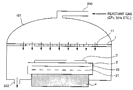
As shown in Fig. 1, in a chamber 101 of a CVD apparatus or an
etching apparatus, a semiconductor wafer 3 to be processed by means of film
deposition or etching is placed. Semiconductor wafer 3 is fixed onto a wafer
holder 2. Wafer holder 2 is attached to a supporter 4. Wafer holder 2
includes an electrostatic chuck electrode 23 for securing semiconductor
wafer 3 by an electrostatic force, and a heater circuit 21 for heating
semiconductor wafer 3. A gas shower unit 1 is placed above semiconductor
wafer 3. Gas shower unit 1 has a plurality of through holes 11 to pass
reactant gas therethrough and includes therein a heater circuit pattern for
heating the reactant gas. The heater circuit pattern is included in gas
shower unit 1 in the form of a conductive layer. Reactant gas for film
deposition or etching gas is introduced from a gas inlet 200 into chamber 101.
The introduced gas passes through a plurality of through holes 11 to be
-11-
CA 02323255 2000-10-17
supplied onto the surface of semiconductor wafer 3. A predetermined film
deposition or etching is done on the surface of semiconductor wafer 3. A
gas discharge outlet 300 is provided for discharging gas from the inside of
chamber 101.
As shown in Fig. 2, in a chamber 102 used for a plasma CVD
apparatus or a plasma etching apparatus, a semiconductor wafer 3 to be
processed by means of film deposition or etching is placed. Semiconductor
wafer 3 is fixed onto a wafer holder 2. Wafer holder 2 is attached onto a
supporter 4. Wafer holder 2 includes a heater circuit 21 for heating
semiconductor wafer 3, a plasma lower electrode 22 for generating plasma in
chamber 102, and an electrostatic chuck electrode 23 for generating an
electrostatic force to secure semiconductor wafer 3. A gas shower unit 1 is
placed above semiconductor wafer 3. Gas shower unit 1 has a plurality of
through holes 11 for passing reactant gas therethrough, and includes
therein a plasma upper electrode opposite plasma lower electrode 22 and a
heater circuit pattern for heating the reactant gas. The heater circuit
pattern and the plasma upper electrode are included in the form of
conductive layer in gas shower unit 1. Gas for film deposition or etching
gas is introduced from a gas inlet 200 into chamber 102, passing through
holes 11 of gas shower unit 1 to be supplied onto the surface of
semiconductor wafer 3. Plasma discharge occurs between the plasma
upper electrode included in gas shower unit 1 and plasma lower electrode 22
included in wafer holder 2. By the gas plasma thus generated, a
predetermined film deposition or etching is performed on the suWace of
semiconductor wafer 3. A gas discharge outlet 300 is provided for
discharging gas from the inside of chamber 102.
Fig. 3 is a perspective view illustrating one embodiment of the gas
shower unit according to the present invention. As shown in Fig. 3, in gas
shower unit 1, a base material 10 of sintered ceramics (hereinafter referred
to as sintered ceramics base material 10) includes therein a conductive layer
where a heater circuit pattern 12 or a plasma upper electrode 14 is formed.
Figs. 4 to G, 9 and 10 respectively show cross sectional structures as
respective embodiments of the gas shower unit according to the present
-12-
CA 02323255 2000-10-17
invention.
Referring to Fig. 4, gas shower unit 1 has a structure in which two
sintered ceramics base materials 10a and lOb are joined. On one sux~ace of
sintered ceramics base material 10a, heater circuit pattern 12 is formed.
Between the one surface of sintered ceramics base matexzal 10a where the
heater circuit pattern 12 is formed and a surface of sintered ceramics base
matex~al 10b, a glass layer or nonoxide ceramics layer 13 is provided to join
sintered ceramics base materials 10a and 10b. A plurality of through holes
11 are formed to pass through sintered ceramics base material 10a, glass
layer or nonoxide ceramics layer 13, and sintered ceramics base material
10b. Heater circuit pattern 12 is formed to avoid through holes 11.
Referring to Fig. 5, conductive paste may be applied between two
ceramics compact pieces to sinter them, thereby producing heater circuit
pattern 12 as a conductive layer within the resultant integrated sintered
ceramics base material 10. In this case, gas shower unit 1 includes no glass
layer or nonoxide ceramics layer as a joint layer.
Referring to Fig. 6, gas shower unit 1 includes therein heater circuit
pattern 12 and plasma upper electrode 14 in the form of conductive layer.
On one surface of sintered ceramics piece 10a, heater circuit pattern 12 is
formed as a conductive layer. Sintered ceramics pieces 10a and lOb are
joined by providing a glass layer or nonoxide ceramics layer 13a between the
one surface of sintered ceramics piece 10a where heater circuit pattern 12 is
formed and sintered ceramics piece 10b. Further, on one sux~ace of a
sintered ceramics piece 10c, plasma upper electrode 14 is formed as a
conductive layer. Between the one surface of sintered ceramics piece lOc
where plasma upper electrode 14 is formed and the other surface of sintered
ceramics piece 10a, a glass layer or nonoxide ceramics layer 13b is formed so
as to join sintered ceramics pieces 10a and 10c. In this way, gas shower
unit 1 having the heater function and the plasma electrode is structured.
It is noted that gas shower unit 1 may include only one conductive
layer sexving both functions of a heater circuit pattern and a plasma upper
electrode. Alternatively, the gas shower unit may be structured to include
therein the plasma upper electrode only.
-13-
CA 02323255 2000-10-17
Fig. 7 is a plan view showing one surface of sintered ceramics base
material 10a where the heater circuit pattern is formed. As shown in Fig. 7,
a plurality of fine through holes 11 are formed in one surface of sintered
ceramics base material 10a. Heater circuit pattern 12 is formed in a zigzag
following a certain pattern, avoiding contact with the locations of through
holes 11. Circular connection terminals 12a and 12b are formed on both
ends of heater circuit pattern 12 for connection to the outside. In addition,
on the one surface of sintered ceramics base material 10a, a groove 15 is
formed for insertion of a temperature sensor as a temperature detecting
unit.
Fig. 8 is a plan view showing one surface of a sintered ceramics base
material where the plasma upper electrode is formed. As shown in Fig. 8, a
plurality of fine through holes 11 are formed in the one surface of sintered
ceramics base material lOc such that the locations of through holes 11
match respective through holes of sintered ceramics base matexzal 10a
shown in Fig. 7. Two through holes 17a and 17b are formed to match, in
location, connection terminals 12a and 12b respectively of the heater circuit
pattern shown in Fig. 7. Plasma upper electrode 14 is formed on the one
surface of sintered ceramics base matexzal lOc to cover almost entire surface
without blocking up openings of through holes 11.
Referxzng to Fig. 9, heater circuit pattern 12 is formed as a
conductive layer on one surface of sintered ceramics piece 10a. Nonoxide
ceramics layer 13a is used to cover the one surface of sintered ceramics piece
10a where heater circuit pattern 12 is fox~xned in order to form a protective
layer for protecting the heater circuit pattern from corrosive gas such as
halogen and the like. In this way, one sintered ceramics piece 10a may be
used to construct gas shower unit 1 including therein heater circuit pattern
12 in the form of a conductive layer.
Alternatively, referring to Fig. 10, heater circuit pattern 12 and
plasma upper electrode 14 may be formed in the form of conductive layers
respectively on one surface and the other sux~'ace of sintered ceramics piece
10a. In this case, nonoxide ceramics layers 13a and 13b covering the
conductive layers respectively are used to form protective layers for
- 14-
CA 02323255 2000-10-17
protecting heater circuit pattern 12 and plasma upper electrode 14 as the
conductive layers from corrosive gas such as halogen and the like. In this
way, one sintered ceramics piece 10a may be used to construct gas shower
unit 1 including therein heater circuit pattern 12 and plasma upper
electrode 14 in the form of conductive layers.
Fig. 11 is a plan view showing, as another embodiment, one surface
of sintered ceramics base material 10a where a heater circuit pattern is
formed. As shown in Fig. 11, connection terminals 12a and 12b are formed
along the same plane on the one surface of sintered ceramics base material
10a to be connected to heater circuit pattern 12. Connection terminals 12a
and 12b extend to a side surface for connection to lines outside the chamber
of the semiconductor manufacturing apparatus. A groove 15 also extends
to the side surface of sintered ceramics base material 10a for inserting a
temperature sensor therein from the outside of the chamber of the
semiconductor manufacturing apparatus. Based on temperature measured
by the temperature sensor, the temperature of the gas shower unit can be
controlled by using a temperature adjustment module provided outside the
semiconductor manufacturing apparatus.
Fig. 12 is a plan view showing, as another embodiment, one surface
of sintered ceramics base material lOc where a plasma upper electrode is
formed. As shown in Fig. 12, a connection terminal 14a is formed along the
same plane on the one surface of sintered ceramics base material lOc to be
connected to plasma upper electrode 14. Connection terminal 14a extends
to a side surface of sintered ceramics base material 10c for connection to
lines outside the chamber of the semiconductor manufacturing apparatus.
A sintered ceramics piece constituting a base material of the gas
shower unit of the present invention can be manufactured by means of a
conventional method. Specifically, a sintering agent is added to ceramics
powder as required, a binder is further added if necessary, and then a
compact piece of that powder mixture is sintered. Since ceramics has heat
resistance as well as corrosion resistance against corrosive gas including
halogen and the like, aluminum nitride, aluminum oxide, silicon nitride and
aluminum oxynitride are preferred. Among them, aluminum nitride is
-15-
CA 02323255 2000-10-17
most preferred because of its heat conductivity and corrosion resistance.
As a method of compacting ceramics powder, any of well-known
sheet forming methods such as doctor blade process, extrusion, press and
the like is used. The compact piece is dried and then undergoes punching
or cutting into a shape which allows the degree of shrinkage after sintering.
Through holes may be made at this stage, or by machining after sintered
pieces are joined.
Binder is removed from the compact piece and thereafter the
compact piece is sintered, preferably at a normal pressure. However, there
is no particular limitation on this pressure. The surface of the sintered
piece may be polished or the sintered piece may be cut if necessary.
However, if the dimension and warp of the sintered piece fall in a
predetermined range, the sintered piece may directly be used as the base
material of the gas shower unit.
In order to form a conductive layer on the surface of the sintered
ceramics piece, paste containing conductive material, for example,
refractory metal such as tungsten, molybdenum and the like or mixture
thereof, or metal or alloy such as silver, silver-palladium, nickel-chromium
and the like is applied by printing on the surface of the sintered piece and
then baked. Between the sintered ceramics piece having the conductive
layer formed thereon and another sintered ceramics piece, a joint element
such as glass, nonoxide ceramics or the like is applied. The ceramics pieces
overlaid on each other are accordingly joined. In this way, the gas shower
unit can be manufactured having the sintered ceramics base material within
which the conductive layer is included.
The manufacturing method discussed above employs so-called post
metalizing method according to which a conductive layer is formed by
applying paste containing conductive material onto a sintered ceramics
piece and then baking it. Alternatively, the co-fire method may be
employed for providing within a sintered ceramics base material a
conductive layer corresponding to a heater circuit pattern or plasma upper
electrode. According to the co-fire method, paste containing refractory
metal such as tungsten, molybdenum and the like or mixture thereof is
-16-
CA 02323255 2000-10-17
applied by printing onto a surface of a ceramics compact piece, another
ceramics compact piece is overlaid thereon to bind them through thermal
compression, the compact pieces are deprived of binder, and then sintering
of the compact ceramics pieces and baking of the conductive paste are
simultaneously performed.
In order to provide within a sintered ceramics base material a
conductive layer serving both of heater and plasma upper electrode
functions, two conductive layers may be formed respectively as a heater
circuit pattern and a plasma upper electrode to manufacture the gas shower
unit as the one having two conductive layers therein. Alternatively, for the
purpose of reducing the size, one conductive layer serving both of heater and
plasma upper electrode functions may be formed.
In order to supply reactant gas uniformly onto the surface of a
semiconductor wafer, preferably through holes each having a diameter of at
least 0.01 mm are formed at a density of not lower than 0.1 holes/cm2,
preferably not lower than 0.5 holes/cm2.
Example 1
5 % by mass of Yttria (Y203) as sintering agent and binder were
added to aluminum nitride powder. They were dispersively mixed and the
resultant mixture was compacted by doctor blade process such that it would
have a thickness of 1.0 mm after sintered. The compact piece was dried
and then underwent punching such that it would have an outer diameter of
350 mm after sintered. 500 through holes were punched out such that they
would each have a diameter of 0.5 mm after sintered. The resultant
compact piece was degreased in nitrogen gas flow at 800°C and sintered
at
1800~C for 4 hours. The upper and lower surfaces of the resultant sintered
piece were polished by using diamond abrasive. By this process, two base
materials of sintered aluminum nitride were produced.
Tungsten powder and sintering agent were kneaded with ethyl
cellulose binder and applied by printing onto one surface of one sintered
aluminum nitride base material. The printed pattern was a linear one with
a line width of 3.0 mm. The linear pattern was shaped in zigzag as shown
in Fig. 7 to avoid the openings of through holes. The sintered aluminum
-17-
CA 02323255 2000-10-17
nitride piece having such a pattern printed thereon was degreased in
nitrogen gas at 800°C and baked in nitrogen gas at 1700 to generate a
conductive layer.
Glass powder was applied by printing onto one surface of another
sintered aluminum nitride base material, and degreased at 500°C. The
sintered aluminum nitxzde base materials were stacked such that the
surfaces respectively having the printed glass powder and the conductive
layer faced each other. The base materials were fixed by a jig made of
molybdenum, and then joined in nitrogen gas at 650°C with a weight
placed
thereon. In this way, the gas shower unit as shown in Fig. 4 was
manufactured that is formed of a sintered aluminum nitride base material
including a heater circuit pattern therein. The gas shower unit was 2.0
mm in thickness.
The gas shower unit thus obtained was incorporated into the CVD
apparatus shown in Fig. 1. A silicon wafer 3 of 300 mm in diameter was
mounted on wafer holder 2 and heated to 700°C. On the other hand, 200 V
was applied to heater circuit pattern 12 of gas shower unit 1 to heat gas
shower unit 1 to 600°C. Then, reactant gas was allowed to pass through
holes 11 to be supplied onto the surface of silicon wafer 3. Temperature
distribution on the surface of silicon wafer 3 measured by a radiation
thermometer was ~0.4°C. Further, a process was conducted for 100 hours
in which a titanium nitride (TiN) elm was formed on the surface of silicon
wafer 3 by using a predetermined reactant gas. In this pexzod, no film was
formed and no film adhered on the sux~'ace of gas shower unit 1 and in
through holes 11. On the surface of silicon wafer 3, no particle of 0.05 ~m
or more in size was generated. After the reaction, power supply to heater
circuit pattern 12 of gas shower unit 1 was stopped, and the temperature of
gas shower unit 1 fell from 600°C to room temperature in 10 minutes.
When voltage of 200V was applied as power supply to heater circuit pattern
12, the temperature of gas shower unit 1 rose from room temperature to
600°C in 6 minutes. The gas shower unit had no crack or the like found
in
temperature increase and decrease.
Example 2
-18-
CA 02323255 2000-10-17
Two base materials of sintered aluminum nitride were produced by
the same method as that in Example 1. A gas shower unit similar to that
in Example 1 was manufactured except that the number of through holes
was 100.
The obtained gas shower unit 1 was incorporated into the CVD
apparatus as shown in Fig. 1. A silicon wafer 3 of 300 mm in diameter was
mounted on wafer holder 2 and heated to 700. 200 V was applied to
heater circuit pattern 12 of gas shower unit 1 to heat gas shower unit 1 to
600. Then, reactant gas was allowed to pass through holes 11 to be
supplied onto the surface of silicon wafer 3. Temperature distribution on
the surface of silicon wafer 3 in this state measured by a radiation
thermometer was t4.0~C. Further, a process was conducted for 100 hours
in which a titanium nitride (Till film was formed on the surface of silicon
wafer 3. In this period, no film was formed and no film adhered on the base
material surface of gas shower unit 1 and in through holes 11. On the
surface of silicon wafer 3, no particle of 0.05 ~,m or more in size was
generated. After the reaction, power supply to heater circuit pattern 12
was stopped, and the temperature of gas shower unit 1 changed from
600°C
to room temperature in 10 minutes. When voltage of 200V was applied as
power supply to heater circuit pattern 12, the temperature of gas shower
unit 1 changed from room temperature to 600°C in 6 minutes.
Example 3
Using the same manufacturing method as that in Example 1, three
base materials of sintered aluminum nitride were produced each having
thickness and diameter respectively of 1 mm and 350 mm and through holes
of the same number.
Tungsten powder and sintering agent were kneaded with binder and
applied by printing onto one surface of one of the base materials of sintered
aluminum nitride. The printed pattern was linear one with line width of
0.5 mm and line interval of 0.5 mm. This linear pattern was shaped in
zigzag avoiding contact with locations of the openings of through holes as
shown in Fig. 7.
Tungsten powder and sintering agent kneaded with binder were also
- 19-
CA 02323255 2000-10-17
applied by pt~inting onto one surface of another one base material of sintered
aluminum nitride. The px~nted pattern was substantially circular one
which did not to block the openings of through holes and accordingly a
plasma upper electrode as shown in Fig. 8 was formed.
The printed patterns respectively on the surfaces of respective two
base materials of sintered aluminum nitride were baked in a similar
manner to that in Example 1 so as to form conductive layers which
respectively form a heater circuit pattern and a plasma upper electrode on
the base materials of sintered aluminum nitride.
The two base materials of sintered aluminum nitride and a
remaining one base material of sintered aluminum nitride were joined in a
similar manner to that in Example 1 by providing glass layer therebetween.
In this way, gas shower unit 1 was manufactured as shown in Fig. G having
therein heater circuit pattern 12 and plasma upper electrode 14. The
obtained gas shower unit had a thickness of 3.0 mm.
Gas shower unit 1 thus manufactured was incorporated into a
plasma CVD apparatus for forming silicon oxide film (Si02 film) as shown in
Fig. 2. A silicon wafer 3 of 300 mm in diameter was mounted on wafer
holder 2 and heated to 300°C. 200 V was applied to heater circuit
pattern
12 of gas shower unit 1 to heat gas shower unit 1 to 600°C. Then,
reactant
gas was allowed to pass through holes 11 to be supplied onto the surface of
silicon wafer 3. Temperature distribution on the sux~'ace of silicon wafer 3
in this state measured by a radiation thermometer was ~0.5°C. Further,
a
process was conducted for 50 hours in which 200 V was also applied to
plasma upper electrode 14 of gas shower unit 1 to generate gas plasma
within chamber 102 and then a silicon oxide film was formed on the surface
of silicon wafer 3. In this period, clogging of through holes occurred which
required cleaning. On the surface of silicon wafer 3, no particle of 0.05 ~.m
or more in size was generated. After the reaction, power supply to heater
circuit pattern 12 and plasma upper electrode 14 was stopped, and the
temperature of gas shower unit 1 fell from 600°C to room temperature in
13
minutes. When voltage of 200V was applied as power supply to heater
circuit pattern 12, the temperature of gas shower unit 1 rose from room
-20-
CA 02323255 2000-10-17
temperature to 600 in 10 minutes.
Example 4
3 % by mass of Yttria (Y20~ as sintering agent and 1 °/ by mass of
calcium oxide (Ca0) as binder were added to aluminum nitride powder.
They were dispersively mixed and the resultant powder mixture was
compacted by doctor blade process such that it would have a thickness of 1.0
mm after sintered. The compact piece was dried and then underwent
punching such that it would have an outer diameter of 350 mm after
sintered. 500 through holes were punched out such that they would each
have a diameter of 0.5 mm after sintered. Tungsten powder and sintering
agent were kneaded with ethyl cellulose binder and applied by printing onto
one surface of the compact piece. The printed pattern was a linear one with
a line width of 2.0 mm. The linear pattern was shaped in zigzag as shown
in Fig. 7 to avoid contact with locations of the openings of through holes.
On the aluminum nitride compact piece having the printed pattern formed
thereon, another aluminum nitride compact piece was overlaid to bind them
through thermal compression. The two aluminum nitride compact pieces
bound by thermal compression were degreased in nitrogen gas flow at 800
and sintered at 1800°C for 4 hours. Accordingly, the printed pattern
and
aluminum nitride were simultaneously sintered. In this way, gas shower
unit 1 as shown in Fig. 5 was manufactured that was formed of base
material of sintered aluminum nitride 10 integrated with heater circuit
pattern 12 provided therein. The thickness of the gas shower unit thus
produced was 2.0 mm.
The resultant gas shower unit 1 was incorporated into the CVD
apparatus as shown in Fig. 1. A silicon wafer 3 of 300 mm in diameter was
mounted on wafer holder 2 and heated to 700°C. On the other hand, 200 V
was applied to heater circuit pattern 12 of gas shower unit 1 to heat gas
shower unit 1 to 600°C. Then, reactant gas was allowed to pass through
holes 11 to be supplied onto the surface of silicon wafer 3. Temperature
distribution on the surface of silicon wafer 3 measured by a radiation
thermometer was t0.5°C. Further, a process was conducted for 100 hours
in which a titanium nitride (TiI~ film was deposited on the surface of silicon
-21-
CA 02323255 2000-10-17
wafer 3. In this period, no film was formed and no film adhered on the
surface of the base material of gas shower unit 1 and in through holes. On
the surface of silicon wafer 3, no particle of 0.05 ~m or more in size was
generated. After the reaction, power supply to heater circuit pattern 12
was stopped, and the temperature of gas shower unit 1 fell from 600°C
to
room temperature in 10 minutes. When voltage of 200V was applied as
power supply to heater circuit pattern 12, the temperature of gas shower
unit 1 rose from room temperature to 600°C in 6 minutes.
Examples 5 to 17
In Examples 5 to 17, through holes were formed by the same method
as that in Example 1 and a polished sintered piece of aluminum nitride was
produced.
Tungsten powder and sintering agent kneaded with ethyl cellulose-
based binder were applied by printing onto one surface of one sintered piece
of aluminum nitride. This was degreased in nitrogen gas at 900°C and
baked in nitrogen gas at 1700°C so as to produce a heater circuit
pattern as
a conductive layer.
On one surface of another sintered piece of aluminum nitride,
powder mixture of nonoxide ceramics and oxide ceramics or oxide ceramics
powder kneaded with ethyl cellulose-based binder, having the composition of
joint layer as shown in Table 2 below, was applied by printing. This was
degreased in nitrogen gas at 900°C. The sintered pieces of aluminum
nitride were stacked such that the surface having the heater circuit pattern
formed thereon faced the surface having the joint layer. The sintered
pieces were fixed by a jig made of carbon and load was applied thereto. In
this state, the sintered pieces were joined by being heated in nitrogen gas at
the joint temperature as shown in Table 2.
In this way, a gas shower unit was manufactured that is formed of
the base material of sintered aluminum nitride including therein the heater
circuit pattern as shown in Fig. 4. The gas shower unit thus produced had
a thickness of 2.0 mm.
This gas shower unit 1 was incorporated into the CVD apparatus
shown in Fig. 1. A silicon wafer 3 of 300 mm in diameter was mounted on
- 22 -
CA 02323255 2000-10-17
wafer holder 2 and heated to 750°C. On the other hand, 200 V was
applied
to heater circuit pattern 12 of gas shower unit 1 to heat gas shower unit 1 to
600. Then, reactant gas was allowed to pass through holes 11 to be
supplied onto the surface of silicon wafer 3. Temperature distribution on
the surface of silicon wafer 3 measured by a radiation thermometer was
~0.5°C. Further, a process was conducted for 100 hours in which a
titanium
nitride (TiI~ film was deposited on the surface of silicon wafer 3 by using a
predetermined reactant gas. In this period, no film was formed and no film
adhered on the surface of gas shower unit 1 and in through holes 11. On
the surface of silicon wafer 3, no particle of 0.05 ~m or more in size was
generated. After the reaction, power supply to heater circuit pattern 12 of
gas shower unit 1 was stopped, and the temperature of gas shower unit 1 fell
from 600°C to room temperature in 10 minutes. When voltage of 200V was
applied as power supply to heater circuit pattern 12, the temperature of gas
shower unit 1 rose from room temperature to 600~C in 6 minutes.
In Examples 1 to 4, no problem occurred when the gas shower units
were continuously used for 1000 hours in a fluorine atmosphere at
700°C.
When the gas shower unit were continuously used for 1000 hours at
750°C,
there was found degradation in one heater out of ten heaters. When the
gas shower units were continuously used for 1000 ours at 800°C,
degradation was found in three out of ten heaters. The reason is
considered to be lowered heater protection effect due to thermal
deterioration of the glass layer.
In Examples 5 and 11, no problem arose when the gas shower units
were successively used for 1000 hours in a fluorine atmosphere at 700
and for 1000 hours at 750°C. However, when the gas shower units were
successively used for 1000 hours at 800°C, deterioration was found in
one
out of ten heaters.
In Examples 6 to 10 and 12 to 17, there was no problem when the
gas shower units were successively used for 1000 hours at any of the
temperatures 700°C, 750°C and 800°C.
Example 18
5 % by mass of Y203 and 2 % by mass of A1203 as sintering agent
-23-
CA 02323255 2000-10-17
were added to silicon nitride powder, polyvinyl alcohol was added thereto as
binder, and they were dispersively mixed by a ball mill using ethanol as
solvent. The powder mixture was spray-dried and then press-formed to
have a shape of 350 mm in diameter 1 mm in thickness after sintered. The
resultant compact piece was degreased in nitrogen gas at 800°C and
sintered at 1550 for 4 hours. The top and bottom surfaces of the
produced sintered piece of silicon nitride were polished by diamond abrasive.
A tungsten heater circuit pattern was formed on one sintered piece
of silicon nitride by the same method as that in Example 1. On another
sintered piece of silicon nitride, a layer of Si02-A1203-based oxide ceramics
having a thermal expansion coefficient of 5.0 x 10'61°C was formed. The
two sintered pieces were stacked and joined by heating them in nitrogen gas
at 1100°C.
Gas shower unit 1 accordingly manufactured was incorporated into
the CVD apparatus shown in Fig. 1. A silicon wafer 3 of 300 mm in
diameter was mounted on wafer holder 2 and heated to 750. On the
other hand, 200 V was applied to heater circuit pattern 12 of gas shower unit
1 to heat gas shower unit 1 to 600°C. Then, reactant gas was allowed to
pass through holes 11 to be supplied onto the surface of silicon wafer 3.
Temperature distribution on the surface of silicon wafer 3 measured by a
radiation thermometer was ~2.0~. Further, a process was conducted for
100 hours in which a titanium nitride (TiI~ film was deposited on the
surface of silicon wafer 3 by using a predetermined reactant gas. In this
period, no film was formed and no film adhered on the surface of gas shower
unit 1 and in through holes 11. On the surface of silicon wafer 3, no
particle of 0.05 ~m or more in size was generated. After the reaction, power
supply to heater circuit pattern 12 of gas shower unit 1 was stopped, and the
temperature of gas shower unit 1 fell from 600°C to room temperature in
20
minutes. When voltage of 200V was applied as power supply to heater
circuit pattern 12, the temperature of gas shower unit 1 rose from room
temperature to 600°C in 15 minutes.
Example 19
2 % by mass of Mg0 was added as sintering agent to aluminum
-24-
CA 02323255 2000-10-17
oxynitride (AIOI~ powder, binder was added thereto, and they were
dispersively mixed. The powder mixture was spray-dried and then press-
formed to have a shape of 350 mm and 1 mm respectively in diameter and
thickness after sintered. The resultant compact piece was degreased in
nitrogen gas flow at 800°C and thereafter sintered at 1770~C for 4
hours.
The top and bottom surfaces of the produced sintered piece of aluminum
oxynitride were polished by diamond abrasive.
A tungsten heater circuit pattern was formed on one sintered piece
of aluminum oxynitride by the same method as that in Example 1. On
another sintered piece of aluminum oxynitride, a layer of Si02-A1203-based
oxide ceramics having a thermal expansion coefficient of 5.0 x 10'sl°C
was
formed. The two sintered pieces were stacked and joined by heating them
in nitrogen gas at 1100°C.
Gas shower unit 1 accordingly produced was incorporated into the
CVD apparatus shown in Fig. 1. A silicon wafer 3 of 300 mm in diameter
was mounted on wafer holder 2 and heated to 750°C. On the other hand,
200 V was applied to heater circuit pattern 12 of gas shower unit 1 to heat
gas shower unit 1 to 600°C. Then, reactant gas was allowed to pass
through holes 11 to be supplied onto the surface of silicon wafer 3.
Temperature distribution on the surface of silicon wafer 3 measured by a
radiation thermometer was t3.0~. Further, a process was performed for
100 hours in which a titanium nitride (TiI~ film was deposited on the
surface of silicon wafer 3 by using a predetermined reactant gas. In this
period, no film was formed and no film adhered on the surface of gas shower
unit 1 and in through holes 11. On the surface of silicon wafer 3, no
particle of 0.05 ~,m or more in size was generated. After the reaction, power
supply to heater circuit pattern 12 of gas shower unit 1 was stopped, and the
temperature of gas shower unit 1 fell from 600°C to room temperature in
20
minutes. When voltage of 200V was applied as power supply to heater
circuit pattern 12, the temperature of gas shower unit 1 rose from room
temperature to 600°C in 15 minutes.
Example 20
One base material of sintered aluminum nitride was produced by the
-25-
CA 02323255 2000-10-17
same method as that in Example 1. Through holes were formed in the base
material of sintered aluminum nitride and a conductive layer of tungsten
was formed in a similar manner to that in Example 1. Paste of aluminum
nitride powder to which 3 % by mass of Yb-Nd-Ca-O-based glass was added
was panted on the suWace of this conductive layer to cover it, and then
baked at 1650°C.
Gas shower unit 1 accordingly manufactured was incorporated into
the CVD apparatus shown in Fig. 1. A silicon wafer 3 of 300 mm in
diameter was mounted on wafer holder 2 and heated to 700°C. On the
other hand, 200 V was applied to heater circuit pattern 12 of gas shower unit
1 to heat gas shower unit 1 to 600°C. Then, reactant gas was allowed to
pass through holes 11 to be supplied onto the surface of silicon wafer 3.
Temperature distribution on the sunace of silicon wafer 3 measured by a
radiation thermometer was ~0.4°C. Further, a process was conducted for
150 hours in which a titanium nitride (TiN) film was deposited on the
surface of silicon wafer 3 by using a predetermined reactant gas. In this
period, no film was formed and no film adhered on the suWace of gas shower
unit 1 and in through holes 11. On the surface of silicon wafer 3, no
particle of 0.05 ~m or more in size was generated. After the reaction, power
supply to heater circuit pattern 12 of gas shower unit 1 was stopped, and the
temperature of gas shower unit 1 fell from G00°C to room temperature in
7
minutes. When voltage of 200V was applied as power supply to heater
circuit pattern 12, the temperature of gas shower unit 1 rose from room
temperature to G00°C in 5 minutes.
Example 21
Five base materials of sintered aluminum nitride were produced by
the same method as that in Example 1. On one base material of sintered
aluminum nitride, a tungsten conductive layer was formed by using the
same method as that in Example 1. Glass layers were provided between
five sintered pieces respectively to join the sintered pieces by the same
method as that in Example 1. In this way, a gas shower unit similar to that
of Example 1 was manufactured.
Gas shower unit 1 thus obtained was incorporated into the CVD
-2G-
CA 02323255 2000-10-17
apparatus shown in Fig. 1. A silicon wafer 3 of 300 mm in diameter was
mounted on wafer holder 2 and heated to 700. On the other hand, 200 V
was applied to heater circuit pattern 12 of gas shower unit 1 to heat gas
shower unit 1 to 600°C. Then, reactant gas was allowed to pass through
holes 11 to be supplied onto the surface of silicon wafer 3. Temperature
distribution on the surface of silicon wafer 3 measured by a radiation
thermometer was t0.6~. Further, a process was conducted for 30 hours in
which a titanium nitride (Till film was deposited on the surface of silicon
wafer 3 by using a predetermined reactant gas. In this period, clogging
was found in through holes 11. Particles were generated on the surface of
silicon wafer 3 and then cleaning became necessary. After this, power
supply to heater circuit pattern 12 of gas shower unit 1 was stopped, and the
temperature of gas shower unit 1 fell from 600 to room temperature in 17
minutes. When voltage of 200V was applied as power supply to heater
circuit pattern 12, the temperature of gas shower unit 1 rose from room
temperature to 600°C in 7 minutes.
Example 22
Two base materials of sintered aluminum nitride were produced by
the same method as that in Example 1. A gas shower unit similar to the
one in Example 1 was manufactured except that the number of through
holes was 30.
Gas shower unit 1 thus obtained was incorporated into the CVD
apparatus shown in Fig. 1. A silicon wafer 3 of 300 mm in diameter was
mounted on wafer holder 2 and heated to 700°C. On the other hand, 200 V
was applied to heater circuit pattern 12 of gas shower unit 1 to heat gas
shower unit 1 to 600°C. Then, reactant gas was allowed to pass through
holes 11 to be supplied onto the surface of silicon wafer 3. Temperature
distribution on the surface of silicon wafer 3 measured by a radiation
thermometer was ~7.0°C. Further, a process was conducted for 100 hours
in which a titanium nitride (Till film was deposited on the surface of silicon
wafer 3. In this period, no clogging was observed in through holes 11.
After this, power supply to heater circuit pattern 12 was stopped,
and the temperature of gas shower unit 1 fell from 600°C to room
-27-
CA 02323255 2000-10-17
temperature in 10 minutes. When voltage of 200V was applied as power
supply to heater circuit pattern 12, the temperature of gas shower unit 1
rose from room temperature to 600°C in 6 minutes.
Example 23
Two base materials of sintered aluminum nitride were produced by
the same method as that in Example 1. A gas shower unit was
manufactured through exactly the same procedure as that in Example 1
except that a conductive layer was formed by applying molybdenum (Mo)
paste onto one base mateizal of sintered aluminum nitride.
Temp er atur a distribution on the sunace of the silicon wafer
measured by the same method as that in Example 1 was ~0.4°C. Similarly
to the process in Example 1, a process of depositing a film was pex~'ormed for
100 hours and no clogging occurred in through holes. It took 6 minutes for
the gas shower unit temperature to izse from room temperature to 600°C
and took 10 minutes to fall from G00°C to room temperature after supply
of
power was stopped.
Example 24
Two base materials of sintered aluminum nitride were produced by
the same manufacturing method as that in Example 1. A gas shower unit
was manufactured by exactly the same method as that in Example 1 except
that paste of silver-palladium (Ag-Pd) was applied to one base material of
sintered aluminum nitride so as to form a conductive layer.
Temperature distribution on the surface of the silicon wafer
measured by the same method as that in Example 1 was ~0.4°C. Similarly
to the process in Example 1, a process of depositing a film was performed for
100 hours and no clogging occurred in through holes. It took 6 minutes for
the gas shower unit temperature to rise from room temperature to 600°C
and took 10 minutes to fall from G00°C to room temperature after supply
of
power was stopped.
Example 25
Two base materials of sintered aluminum nitride were produced by
the same method as that in Example 1. A gas shower unit was
manufactured by exactly the same method as that in Example 1 except that
-28-
CA 02323255 2000-10-17
paste of nickel-chromium (Ni-Cr) was applied to one base material of
sintered aluminum nitride so as to form a conductive layer.
Temperature distribution on the surface of the silicon wafer
measured by the same method as that in Example 1 was t0.4°C. Similarly
to the process in Example 1, a process of depositing a film was penormed for
100 hours and no clogging occurred in through holes. It took 6 minutes for
the gas shower unit temperature to rise from room temperature to 600°C
and took 10 minutes to fall from 600°C to room temperature after supply
of
power was stopped.
Examples 26 to 30
By the same manufacturing method as that in Example 1, one base
material of sintered aluminum nitride and another base material of sintered
aluminum nitride having a tungsten conductive layer formed thereon were
produced. The two sintered materials were joined in nitrogen gas at
700°C
using glass of respective thermal expansion coefficients 2.5 x 10'6/°C,
3 x 10'
6/°C, 5 x 10'6/°C, 7.9 x 10'6/°C and 10 x 10'6/°C
for respective examples. The
target temperature increasing rate was 30 minutes/600°C or less. Crack
after 35 minutes, crack after 6 minutes, no crack within 6 minutes, crack
after 8 minutes, and crack after 80 minutes were observed in respective
examples.
Comparative Example 1
Two base materials of sintered aluminum nitride having through
holes were produced by the same method as that in Example 1. Glass
powder was applied by printing onto one surface of one of the base materials
of sintered aluminum nitride. After the one surface of the sintered
aluminum nitride base material was degreased at 500°C, another sintered
aluminum nitride base material was overlaid thereon. The base materials
were fixed by a jig made of molybdenum, a weight was placed thereon, and
they were joined in nitrogen gas at 650°C. A gas shower unit 1 as shown
in
Fig. 13 was accordingly manufactured. Glass layer 13 as shown in Fig. 13
joined sintered aluminum nitxzde base materials 10a and 10b. A plurality
of through holes 11 were made in gas shower unit 1.
Gas shower unit 1 thus produced was incorporated into the CVD
-29-
CA 02323255 2000-10-17
apparatus as shown in Fig. 1. A silicon wafer 3 of 300 mm in diameter was
mounted on the surface of wafer holder 2 and heated to 700. Reactant
gas was then allowed to pass through holes 11 of gas shower unit 1 to be
supplied onto the surface of silicon wafer 3. Terriperature distribution on
the surface of silicon wafer 3 in this state measured by a radiation
thermometer was t15~. Further, a process was conducted for 100 hours in
which a titanium nitride film was deposited on the surface of silicon wafer 3.
In this period, there was no film observed which adhered on the surface of
the base material of gas shower unit 1 and in through holes 11, and no
clogging was found in through holes.
The temperature of gas shower unit 1 was gradually increased by
the heat radiated from underlying wafer holder 2, and it took 180 minutes
for the temperature to reach 600°C. When supply of power to wafer
holder
2 was stopped, the temperature of gas shower unit 1 fell to room
temperature in 15 minutes.
Comparative Example 2
5 °/ by mass of Yttria (YZOg) as sintering agent and binder were
added to aluminum nitride powder. They were dispersively mixed and the
resultant mixture was press-formed by using a mold such that it would have
an outer diameter of 350 mm and a thickness of 5 mm after sintered. In
this way, two compact pieces of aluminum nitride were produced. Between
these two aluminum nitride compact pieces, a molybdenum wire of 0.5 mm
in diameter was arranged in a spiral shape at a pitch of 10 mm such that the
outer diameter of coil winding was 5 mm. In this state, they were hot-press
sintered at 1850°C. After sintering, through holes each having a
diameter
of 0.5 mm were formed one by one in the resultant base material of sintered
aluminum nitride by using a micro diamond drill, the through holes being
formed to avoid the region where the heater coil was arranged. 50 through
holes were produced in the base material of sintered aluminum nitride
accordingly. A gas shower unit 1 having a heater coil wire 16 in sintered
aluminum nitride base material 10 was manufactured as shown in Fig 14.
Gas shower unit 1 accordingly manufactured was incorporated into
the CVD apparatus as shown in Fig. 1. A silicon wafer 3 of 300 mm in
-30-
CA 02323255 2000-10-17
diameter was mounted on wafer holder 2 and heated to 700°C. On the
other hand, 200 V was applied to heater coil wire 16 of gas shower unit 1 to
heat gas shower unit 1 to 600°C. Then, reactant gas was allowed to pass
through holes 11 to be supplied onto the surface of silicon wafer 3.
Temperature distribution on the surface of silicon wafer 3 measured by a
radiation thermometer was t10°C. Further, a process was conducted for 8
hours in which a titanium nitride film was deposited on the surface of silicon
wafer 3. In this period, films adhered on the surface of the base matexzal of
gas shower unit 1 and in through holes and clogging occurred in through
holes. Further, particles were generated on the surface of silicon wafer 3,
and cleaning became necessary for gas shower unit 1. After this, power
supply to heater coil wire 16 was stopped, and the temperature of gas
shower unit 1 fell from 600°C to room temperature in 180 minutes. When
voltage of 200V was applied as power supply to heater coil wire 16, the
temperature of gas shower unit 1 rose from room temperature to 600°C in
30 minutes.
Comparative Example 3
Six base materials of sintered aluminum nitride having through
holes formed therein were produced by the same method as that in Example
1. On one of the sintered aluminum nitx~de base materials, a conductive
layer of tungsten was formed by the same method as that in Example 1.
The six sintered materials were joined with glass layers interposed
therebetween according to the same method as that in Example 1.
Gas shower unit 1 thus obtained was incorporated into the CVD
apparatus shown in Fig. 1. A silicon wafer 3 of 300 mm in diameter was
mounted on wafer holder 2 and heated to 700°C. On the other hand, 200 V
was applied to a heater circuit patter 12 of gas shower unit 1 to heat gas
shower unit 1 to 600°C. Then, reactant gas was allowed to pass through
holes 11 to be supplied onto the surface of silicon wafer 3. Temperature
distribution on the surface of silicon wafer 3 measured by a radiation
thermometer was ~0.8°C. Further, a process was conducted for 14 hours
in
which a titanium nitride (TiN) film was deposited on the surface of silicon
wafer 3 by using a predetermined reactant gas. In this period, films
-31-
CA 02323255 2000-10-17
adhered on the surface of the base material of gas shower unit 1 and in
through holes and clogging occurred in through holes. Further, particles
were generated on the surface of silicon wafer 3, and cleaning became
necessary for gas shower unit 1. After this, power supply to heater circuit
pattern 12 was stopped, and the temperature of gas shower unit 1 fell from
600 to room temperature in 30 minutes. When voltage of 200V was
applied as power supply to heater circuit pattern 12, the temperature of gas
shower unit 1 rose from room temperature to 600°C in 15 minutes.
The structures of gas shower units according to Examples 1 to 30
and Comparative Examples 1 to 3 as well as respective results are shown in
Table 1. It is noted that, in Table 1, "W posmeta" means that the
conductive layer containing tungsten is produced by the post metalizing
method, "W co-fire" means that the conductive layer containing tungsten is
produced by the co-fire method, and "Mo coil/HP" means that a sintered base
material is produced through hot-press sintering with a molybdenum coil
-32-
wire interposed between compact pieces.
CA 02323255 2000-10-17
~ ~r o m ua ~n o o Wit; cc o Wit; ~r ~r o 0 00
~~~I o~o00~imoor:o00 ' ' ' ' ' X00
u~ ~.c~ u~ u~ ~ u~ u~ '~' u~ u~ u~ u~ ~c~ ~ m ~n ~ ~ u~ ~ u~
~ G~1
;~~ ~ ~~ M ~~ zo,~~~~~~~~~~~ ~ ~~
U
°~q,a; 0 0 0 0 0 0 0 0 0 0 0 0 0 0 0 0 0 0 0 0 0
-d ~ ~ ~~ ~ ~ .3
~ o as U
m v~ v? u~ r~ vi v~ v~ . v~ O
"d O O O [g O O O O O O , .~"i.., ~n O O O O o
a.~w a.. wa.~wwa~a~ zwwa.~wa..~ x ~w
--r c~ m d~ ~ ~ ~ c°~ ~ ~ ~ c~~t ~ ~ ~ ~ ~ c~ ,-'
°' . ~.a'.
w
CA 02323255 2000-10-17
Table 2
Exam Joint La er Joint Tem
1e
40%A1N-X60%(Ca-Al-Si-O) 1600C
6 50%A1N-E-50%(Ca-Al-Si-O) 1600C
7 70%A1N-E-30%(Ca-Al-Si-O) 1600C
8 90%AlN-f-10%(Y-C~-O) 1650C
9 90%A1N-f-10%(Yb-Nd-Ca-O) 1650C
90%A1N-f-10%(Yb-Nd-Ca-O) 1650C
11 97%AlN-I-3%(Yb-Nd-Ca-O) 1650C
12 40%Si N +60%(Ca-Al-Si-O) 1600C
13 50 %Si N -f- 50 % (Ca-Al-Si-O)1600C
14 70%Si N -E-30%(Y-Al-Mg-O) 1600C
90%Si N -f-10%(Y-Al-Mg-O) 1650C
1G 90%A1N-f-10%(Y-Al-Mg-O) 1650C
17 Yb-Nd-Ca-O 1650C
Although the present invention has been described and illustrated in
detail, it is clearly understood that the same is by way of illustration and
5 example only and is not to be taken by way of limitation, the spiizt and
scope
of the present invention being limited only by the terms of the appended
claims.
-34-