Note: Descriptions are shown in the official language in which they were submitted.
CA 02323474 2000-09-11
, 1
Transparent and semitransparent diffractive elements, particularly holograms
and their
making process.
Background of the invention
This invention relates to a improvement of transparent and semitransparent
diffractive
elements and more particularly to a transparent and semitransparent type
holograms and
their making process. These diffractive elements are themselves transparent or
semitransparent in visible (VIS) andlor near infrared (NIR) spectral region
and yet are also
endowed with the characteristics of a reflection type elements being observed
under suitable
angle. It means that reproduction in the transparent or semitransparent
element of the
present invention is effected only within specific reproduction angle range,
while no hologram
is recognised at other ordinary angles. This leads to4 the advantage that
there is no visual
obstruction of the article on which the diffractive element is laminated. Fig.
1 shows the basic
constitution of the transparent or semitransparent diffractive element
according to the present
invention.
State of the art
Demand for holograms has grown not only as the way of the record of sound or
information
but as the elements used in such activities of human beings as advertisement,
security
sector, safety technique, protection of product originality, money counterfeit
protection etc.
It is well known that one of the following replication technologies is usually
used for mass
production of any diffractive elements in suitable polymer materials - hot
embossing, injection
moulding and casting.
Relief microstructure (master copy) is produced by one of the many high
resolution fabrication
technologies, the most commonly used being holographic exposure of suitable
photosensitive
material, including chalcogenides (US 3,825,317), direct writing with focused
laser and e
beam, optical photolithography with subsequent wet or dry etching.
In most cases, a nickel shim or stamper is electroformed or replica is
produced through
casting into epoxy resin. These replicas are used for own mass production of
copies into
polymers using injection moulding (CD fabrication), casting (production of
gratings for
spectrophotometers) or hot embossing, for example into transparent foil (M.T.
Gale: J. of
Imaging Science and Technology 41 (3) (1997) 211).
Transparent polymeric materials such as polyethylene with index of refraction
n = 1.5 - 1.54,
polypropylene n = 1,49, polystyrene 1,6, polyvinyl chloride 1,52 - 1,55,
polyester resin 1.52
1,57 etc. (for more examples see US patent 4856857) or copolymers (for
correction of index
of refraction) can be used for transparent or semitransparent holograms and
other diffractive
elements production. Low refraction index value of these polymers or
copolymers prepared
from them determines their low reflectance (R about 4 %), hence the
holographic effect of
diffractive structure developed in layers of these polymers is insufficient
(US patent
4856857). Under the term "holographic effect" used in the following text we
will understand
CA 02323474 2000-09-11
' . . 2
the phenomenon, that the hologram is very intensive in reflected light at
suitable angle of
observation. Low reflected intensity and thus the drawback of poor brightness
of diffractive
element recorded in the polymer layer is usually passed by forming a thin
metallic film
(generally AI) on the relief forming face of transparent polymeric layer (M.
Miler: Holography -
theoretical and experimental fundamentals and their application, SNTL, Prague
1974 (in
Czech); M.T. Gale: J. of Imaging Science and Technology 41 (3) (1997) 211).
Strong improvement of brightness achieved at the cost of loss of the
transparency is the
main drawback of such technique. Transparency or at least semitransparency of
diffractive
element is required or desired in many applications (for example protective
diffractive
elements on banknotes, identity cards with photo etc.). Some technical
applications of
diffractive elements are directly conditioned by transparency or
semitransparency of created
element ( for example microlense array for CCD cameras, polarising filters
etc.).
It is further known that to preserve (or to decrease only partly) the
transparency of diffractive
element and at the same time to improve holographic effect of the hologram
recorded in the
polymeric layer (further called layer 1), it is necessary to cover layer 1 by
other transparent
layer (further called layer 2) of different material (further called
holographic effect enhancing
material) which has in general different index of refraction n (i.e. higher or
lower ) than
material of the transparent layer 1 (US patent 4856857, US patent 5700550, US
patent
5300764). The higher difference in index of refraction of polymeric bearing
layer 1 and
holographic effect-enhancing layer 2, the higher holographic effect can be
achieved (US
patent 4856857).
It is as well known that very thin layer (with thickness to the limit 20 nm)
of suitable metal
(e.g. Cr, Te, Ge) can be used as such layer 2 deposited on the transparent
layer 1 in which a
hologram has been hot-formed. Such very thin metallic layer being used,
relatively high
transparency is preserved. Relatively strong enhancing of holographic effect
can be achieved
when the index of refraction of deposited metallic layer is either
significantly lower (e.g. Ag n =
0,8; Cu n = 0,7) or significantly higher {e.g. Cr n = 3,3, Mn n = 2,5, Te n =
4,9) than index of
refraction of transparent layer 1 ( n about 1,5), (US patent 4856857). Such
thin metallic layers
are deposited at transparent, diffractive element bearing layer 1 by vacuum
deposition
technique. The drawback of the application of thin metallic layer as
holographic effect
enhancing material is relatively high melting point of these materials and
therefore difficult
evaporating of many of these metals. An additional drawback is high absorption
coefficient of
metals. Already slight deviations in the thickness of evaporated metal layer
implicate
significant deviations in the transmissivity of the system (layer 1 - bearing
diffractive element
+ layer 2 - metal) and moreover upper limit of the permissible thickness is
very low {it
depends on the metal, but in general it must not exceed 20 nm (US patent
4856857)).
According to our measurements evaporation of either 10 nm thick Cr layer or 4
nm thick Ge
layer on the polymeric layer decreases its transmissivity down to about 30 %
(see Fig. 2).
In the present art, oxides of metals (e.g. ZnO, PbO, Fe203, LaZ03, Mg0 etc.),
halogenide
materials (e.g. TICI, CuBr, CIF3, ThF4 etc.) eventually more complex
dielectric materials {e.g.
CA 02323474 2000-09-11
:::::::.:::::::::::::::::::::.:;:> _ . .
.::::::::::.::.::.:::.::::>:,>::::::.:;:::.::.:>::.::::.:>: . . , , .,
...,~...::.::::>:::::.:.-:::::::::::::::::
::>:::.::.:;::.:::;:.:;::o:.::..:::.:..: I 1 . . _ _ . ::....:...:. , . ., .
.. .: . .: . .: . :.) ) , r ) , + : ::. ...: :.::.:::::.:;:::::::
Rl.: .,;.;.:. ..;..::: .:.: . ..:l6NCHE.N )4_ __ _._ 4' _ 4 . ~ .
..::.~::::::.:~ ::.:::-. .. ; .: > .:::::: __-. 243F~_~4 49 f :.:: ..~.
.:::.:;::::.:>:;:;:;:
::: ::: : ~ ::: :~~': ; ..: ::: <: ::::. ~ ~ :. ~ ~ .~ . : ~ . v.~::
:~~:::::::::::::::::
:: ~ .:. . . . .- :, v: :::: ~:::: .:::~ ::
:::::::.::':.:::.::.::.:::.:::.:i::::~'..
:::::.::.:.:::::::Q..:Q:
::.~::::::::::::::::::.::.:.::.::.:::;::.:::>:::.::::... P
T/C:...:.,..:.:..:.._..._...._..._......
3
~Teo.asNbo.ss~. Bi,(Ge0J3, RbHzAsO, att.) are used single or possibly in
several layers
deposited crisS-cross as holographic effect enhancing layers (US patent
485685'n. The
drawback of the appheatlon of these materials is the fact that their index of
rofraation values
. are very close to the index of refraction of transparent polymeric layer 1
(e.g. index of
refraction values ate 1,5 for ThF4, 1,5 for SIOz, 1,6 for Rii03, 1,6 fot
RhH~4s0, ete_) (US
patent 488857). Accordir~ly an ampl>flcation of holographic effect is
relatively low. Many of
these materials require again relatively high temperature for their
evaporation and not least
some of them are quite expensive or hanlly prepareable, what obstructs their
mass
appticatian,
Further tt is icnowrt, that binary chaloopenides of zinc and cadmium as well
as compounds
Sb~S= and PbTe (US patent 4856857), eventually multilayer systems of these
chalcogenides
with oxides or halides (US Patent 5700550) or muklfayer system ZnS and NagAlFs
(US
patern 5300764) can be used as holographic effect enhancing. These materials
are endowed
with satisfactory index of r~efradion values (e.g. 3,0 for SbzSs, 2,fi for
ZnSe, 2,1 for ZnS). But
short wavelength absorption edge of many of these materials (e.g, SbiSs, CdSe,
CdTe,
ZnTe) ties within near IR region only and these materi$Is era characterised by
high values of
_ absorption coefficient in VIS. Similarly with metal layer used as layer 2,
only very thin layers
. of these materials can be used as holographic effect enhancing layer 2 to
achieve at least
sernitransparency of final prndud. Transparency Is again signifrcantty
influenced by
thickness deviations. Additional significant drawback of these materials is
their difficult
vaporization (again similarity with metals) given by their high values of
their milting points
Ta alto - ZnS 1700 °C, beta - ZnS 1020 °C, Zn8e >1100 °C,
ZnTe 1238 °C, CdS 1750 °C,
CdSe > 1350 °C, CdTe 1121 °C, PbTe 917 °C) (Handbook of
Chemistry and t~hysics 64th
Edition 1983184).
In the present art the process according to the scheme given in Fig. 3 is
usually used in the
mass production of lransparent diffracttve etemer>ts. Firstly a diffractive
pattern is made in
' the layer 1, after it a thin dielectric or metallic layer is evaporated
(perpendiarlarty or under
. . specific incidence angle) a subsequently this evaporated layer is
overlapped or laminated by
another polymeric layer (M.T. Gale: Journal of Imaging Science and Tec~noiopy
41 (3)
(1997) 211). As above mentioned materials (metals, their oxides, halides,
binary
chalcogenides of Zn and Cd, SbaS3 and Pb1'e) are used as layer 2 in the
production of
diffractive elements by this way, the method has the same drawbacks, e_g. high
melting
temperatures determine difficult deposition, even small deviations in the
thickness cause
large deviations in the transmissivity, comparable index of refraction of many
of these
materials with index of retraction of polymeric layer 1, eventually full non
tranaparoncy in
VIS.
. Further it is known thst holographic tape (relief phase holograms shaped in
a vinyl tape)
have improved scratch resistance being covered with such materials as waxes,
polymers
and inorganic Compounds, besides others arsenic sulphide can be used (US
patent 8 703
407). In addition the coating enables tapes to be lubricated and enables tapes
to be used in a
:::.::
AMENDED SHEET v»~=v
CA 02323474 2000-09-11
,.....:.,.,.,.:.--..-.".::., - . . .
::.:::::::::.::::.:.::.:>:::;::.::.:;::.::.::.:>:::.::-.::.::.: , ~ . ~.,
:,.",.,::::::::;::::::::::.:::::::::::::::
.......................................
.:::;::.:>::::::.:;::::.:::. f . - _ ..:....::.;....:...,......::.:.:....:-
:::..:...:....: ~ ~ -.~
Rc::.:>:::.:....::-::.:......:....: .:?~:ENCHFI~ 04_ _ __ . 4 _ 4_ _ a ~:...:.
...:: :..::~ .: .. .. : .. : .: ~ -._Z4a~_74 +49 a : >:
.:....::,,:.::.:::.:;::< ::.
v ; <. : <:.,. :. .: :: : : : :. ::.. : ~ ::. . . .. w : , :. : ; :::
~~~~:::::::::::::
~. .: .. r :. .. W : ' : :. .. .: :: :.::::: ~ >:::-::::.: >::.: >::::-::.:
~:::.:
. .>~~4:: ~4. .~Q~Q :. ;:..::.::.::..:.::.:::::. ::::::::. :. ::::::::.::::-
..:.:.:. PCT/C......_ ....: .- ... ..._.. _ ........
H"
liquid gate tape transport mechanism. In order to maintain the same
diffraction efficiency as
an uncoated tape, the minimum depth of this coating must be greater than the
maximum
peak-to-valley depth of any corrugation (US patent 3 703 407)_
Subject matter of !he invention
The present invention does away with the drawbacks of the present-day
techniques of
transparent and semitransparent diffradive elements production.
Transparent and semitransparont diffractive elements, particularly holograms,
consisting at
least of two layers with a different index of refraction, whereof a first
bearing layer (1) is a
transparent polymer or copolymer having index of refraction lower than 1,7 and
on said first
bearing layer is deposited a second to exposuro sensitive holographic effect
enhancing high
retraction index layer (2) constituted by substances based on chalcogenides
with an index of
refraction higher than 1.7 and a melting temperature lower than 900 °C,
characterized in that
the first diffractive pattern is mechanically shaped in the bearing layer (1)
andlor in the the
high refraction index layer (2) and at laser one further second diffractive
pattern is formed in
the high refraction index layer (2), constituted by substances based on
chalcogenides
comprising at least one of the elements from the group sulphur, selenium,
tellurium, the said
chalcogenide based substances being selected from the group of binary, ternary
and even
more complex chalcopenide and/or chalcvhalogenide systems, containing, fn
addition to S or
Se or Te, as a more electropositive element some of the elements Cu, Ag, Au,
Ng, B, AI,
Ga, In, TI, Si, Ge, Sn, Pb, N, P, As, Sb, Bi.
..;. Chalcogenides based matters can contain further transient metal andlor at
least one rare
earth element, e.g. Pr, Eu, Dy.
Transparent or semitransparent diffractive element can further consists of
other layers e.g.
protective layer, adhesive layer, fragile layer, anchor layer. Protective
layer protects layer 2
or layer t against environmental effect or against undesirable effect of
consecutive e~osure
by tN light and improves reshstivity of the final product. The layer can
either be permanent
part of the hologram or of the diffiactive element or can be removable.
Adhesive layer
allows unrepeatable or repeatable anchoring of the hologram or other
diffractive element on
protected article, printed document etc. The function of fragile Isyer is to
adhere the upper
layer and the lower layer and yet effect destruction of diffractive element
during peeling for
the purpose of tor8ery. Anchor Layer is used to improve adhesivity of
diffrectiye element to
the base supportirtg sheet or to releasable sheet in the case of application
as seal, sticker,
Isbel ate.
Transparent layer 1 can be inseparable part of Some larger product, in such
case the high
refraction index layer ~ can be for example sprayed on the layer 1.
Procedure of transparent diffradive elements production consists of the
formation of the first
diffractive patem in a bearing Isyer 1 and subsequent deposition of high
refraction index
.~ f
layer 2, which is formed with a chalcogenido based matters of differont
compositions. The
deposition of dffterent chalooge~ide based matter3 can be consecutive or
simultaneous and
AMENDED SHEET
CA 02323474 2000-09-11
...... . .... .................................................
:::::::::::::::::::::
.. ...". ..._.. .. . _ . .
.::.:>:::::.::::.::::.:::::::;:::;::::.::.:::::::.:::::: . . r.
nnror,:::.:::::.::::::>:;.:-::::::::::::<:_
:::.:::.:>:>:::::::::::::.~.:~.:;:;::' . ._ _ ,
.:....:...:...:....:....::.:...:'....:'..:...: w' -. . ~ ~ :.. . .. ..: ::::
RC::.::::.::.:::.::::.:>:'::.:':. ..::..::IIEI~CHhN U4 4 _ 4 _ .0 . :.:
...:... .: :.:: ... . . .. : .. : .: :a_ 2.. 2455274 +4,i F' : . .... .
::.:::::::.:::.::'.::.:
~ :::, :. : ':. ::: . . . _ _ _ .. . <:':: :.. ~ :: ~ . , .., .. .: . : : :
:::~Ea~~~:~:::::::::::::::::
'.: :. .~ : ~. : . : ' :: .i .: :'::::::::i::-:~:::ni::.:i::::::::.:
~~..;~D~.:~~i~.. :.:'.::.::::::::::::::::::.::::::....::::::.~:._:._::::. P
T/C......._..._.:.:_.~ ._ _ .......
S
than the second diffractive patterns are formed in the said to exposure
sensitive high
refraction index layer 2.
Alternative way of transparent and semitransparent diffractive elements
production is firstly
to deposit high refraction index layer 2 on bearing layer 1 and only after
that to originate a
required the first diffractive pattern into high refraction index layers at
elevated temperature
for example using hot embossing technique. If the depth of diffractive pattern
is greater than
the thickness of high refraction index layer 2 (very common situation) ,
pradicsfly identical
product (Fig. 1) is obtained as when the previous procedure is used. If the
ernbossinp depths
are lower than thickness of high refraction index layer, the layer 1 operates
as carrier of high
refraction index layer 2 only. After that the second diffractive patterns are
formed in the said
to exposure sensitive high refraction index layer 2.
Hmh refraction index layer can be deposited on a prev'rously coloured layer 1
and thus
through the combination of their colours (colour of layer 2 depending on the
composition and
thickness used a requirod colour effect of transparent or semitransparent
diffractive element
can be achieved.
High refraction index layer 2 can be deposited either a1 low pressure e.g.
using vacuum
evaporation, sputtering or chemical vapour deposition (CllO) technique or at
normal
pressure as solution of chalcogenida based matters using e.g. spraying,
painting or spin
' coating method.
2.o The composition of high refraction index layer 2 loaned with some
chalcopenide based
matters can be modified by exposure or annealing induced diffusion of metals
and/or by
halogens andlor oxygen, which are implanted into layer 2 by interaction of the
layer 2 with
halogen vapours or oxygen or by air hydrolysis.
The sensation of the first diffractive pattern shaped mechanically in layer 1
andlor Isyer 2 is
modified by second diffractive pattern formed in layer 2 by exposure andlor
annealing andlor
by selective etching.
Exposure with radiation of suitable wavelength and intensity (values depend on
the particular
composition of high refraction index layer (2), e-beam, ions, X ray radiation
etc.) w
annealing originates structural changes in high refraction index layer or it
originates even
3U changes in its chemical composition (e.g. diffusion of metal, which 1s in
direct contact with
high refraction index layer, hydrolysis, oxidation). Thereby a change of the
value of index of
refraction of layer 2 takes place (d usually increases) and thus the
difference between values
of index of refraction of bearing layer t and high refraction index layer 2 Is
modified. It
results in a different optical perception of the product. A chemical reaction
induced by
33 exposuro or by annealing, e.g. with surrounding atmosphere, can result in
the transformation
of chalcogenide material into fully different compound (e.g. oxide); the
product of such
reaction must again satisfy the condition, that its index of refraction is
higher than 1,7.
Local exposure through the mask or holographic exposure or local anttealinp
can pn~duee a
rtcord of the further second diffradive pattern into the high refraction index
layer 2; the
4tf record can be either amplitude (based on different absorption ooeffideM of
exposed and
::':.....:...:.::<:.::.:...:::.....:.::;:::....::::::.~::::.:::::: AMENDED S E
CA 02323474 2000-09-11
................................................. ~ . ~
::.::::::::::::::.::::::::::::.
.,.......:.::..-.:.::.:z.~..t,.:.:::~..., . ~ . . . . .
::>::.::::::.:::>::.:::::::.:::.:::.::.:::.:;::.:::.:.._.:.:.~: r n
~~~::~~:::_::;::;:;:::::.::;::::_::::::::::
;::.:::.::::::::::.::::.::.::.: .. . _ 4_ U ..:....:.:....;....:.......:-
...:....,,..: :: ) 2 ~43.~5274-~ +4J P :::::::::.,::.::
2('............................ .. _fv,(.HEfv U4 4 .. ....
:~:: ~ :w : .:lo-' : ': :~ ::: : . '' ': ::::::::::'::
:: .:. .:. . . :: ::::::.~: :.:::.:: .::::.:::::::.~:::::: :.:::.~:::.~ -
::::::::: ::::.::.::.:>:::::::.::~:::_
C _~ Q _ :: :..:: :..... PCT/C....._ .._ . _ . _ _
Ss
unexposed part of layer 2j or phase type based on either different values of
index of
refraction of exposed and unexposed parts of layer 2 or based on different
thickness of
exposed and unexposed parts of the layer 2 (differoM thickness can be aohieved
not only
directly during exposure but also by consecutive etching of layer 2 by using
well-known
S methods); even here can be used the phenomenon of local photoinduced
diffusion.
hydrolysis, oxidation etc. and the matter of high refection index layer 2 can,
in the place of
local exposure or annealing change its chemical oompositlon: resulting record
in the high
refraction index layer 2 can partly modify visual perception of the hologram
and in addition it
can be seen in view-through.
As index of refraction values of majority of chalcogenides exceed the value n
= 2,
application of chalcogenides layers as holographic effect enhancing layer 2
deposited on the
transparent polymeric layers 1 with n < 1,7 results generally in a signtflcant
visual perception.
The transparency of final hologram or other diffractive element can be
influenced through
the thickness of layer 2.
Another important adverttage of chalcogenide materials is the fact, that they
can be
synthesised in many systems in amorphous state and their glass forming regions
are
rolatively wide. Being amorphous, these materials have not only very low
scattering losses,
but the possibility to prepare even nonstochiometric compounds takes place,
t3radual mutual
~'~.:.:..,~'~.;:,,~~..:::: AMENDED SHEET ..::::
::::~.:~::::<::::::...::::::<;:::::::::::::::::::::::::::. >°~.
.:';:..~::.:::..:>:.;..r... ,::..T :.::,:.:~:.:::::.;::':,v>
CA 02323474 2000-09-11
6
substitution of elements (not only S, Se and Te) in the composition of
amorphous
chalcogenides causes continuous changes in their index of refraction and
reflectivity. Thus
enhancement of holographic effect can be "tailored".
As a result of gradual mutual substitution of elements in the composition of
amorphous
chalcogenides arise gradual changes of their optical gap E9 °' values
(e.g. As4oS~ E9 ~ = 2,37
eV, As4aS~Seza 2,07 eV, As4oSe~ 1,8 eV) followed by gradual changes in the
position of
short wavelength absorption edge. Thus the colour (for given thickness) of
layer 2 can be
changed as well and transparent and semitransparent systems of different
colours endowed
with high holographic effect can be produced. So even colourless polymeric
layers 1 can be
used for production of transparent or semitransparent diffractive elements of
required colour
using one (or more) chalcogenide based layer of suitable composition as a
layer 2. Thus
composition and thickness of chalcogenide layer 2 influence significantly the
transparency of
final product (hologram) (Fig. 4) and reflectivity (Fig. 5) and thus intensity
of holographic
perception (it increases with the reflectivity of layer 2).
Amorphous chalcogenides are mainly as thin layers photosensitive to exposure
with radiation
of suitable intensity and vawelength (given by composition of the layer), e-
beam, ions etc.
This property enables us to provide an supplementary correction of index of
refraction,
reflectivity and transmissivity of high refraction index thin layer using
exposure induced
structural changes (Fig. 6), by exposure induced reaction of photosensitive
chalcogenide
layer with metal (e.g. Ag) (Fig. 6) or with gas (O2, air humidity) induced
transformation into
different chemical substance, which must satisfy the condition that n > 1.7.
Similar effect can
be achieved by annealing.
If exposure or annealing are local only, procedures mentioned in the previous
paragraph can
result in the formation of an image (including holographic one) in the high
refraction index
layer, which can partly modify visual perception of the hologram and in
addition it can be seen
in view-through. Sectional views of structures developed using photoinduced
structural
changes and photoinduced metal diffusion are presented in Fig. 7 and 8.
Further advantage of above mentioned chalcogenides are their low melting
temperatures
(usually 100 - 300 °C). They can be therefore deposited by worldwide
commonly used
vacuum evaporation method. As the values of absorption coefficient in the
region behind
short vawelength absorption edge are low, even possible small deviation in the
thickness
influences much less the holographic effect enhancing than when thin metallic
layers are
used. Large areas of chalcogenide layers can be formed relatively easily using
corresponding
vacuum evaporation equipment. The thickness of the chalcogenide layer 2 can be
adjusted
by synchronising the evaporation rate with the feed speed of transparent
bearing layer 1.
Further advantage of amorphous chalcogenides is the fact, that mass production
of
chalcogenides of many compositions exist worldwide and they are thus
immediately
commercially available at affordable price.
CA 02323474 2000-09-11
7
Brief description of the drawings
Fig. 1 Sectional view of the diffractive element of the present invention, 1 -
transparent bearing
polymeric layer with n, < 1,7, 2 - high refraction index chalcogenide based
layer with n2 > 1,7
Fig. 2 Optical transmissivity T and reflectivity R of holograms produced by
deposition of thin
high diffractive index layer 2 formed by Cr or Ge on polyethylene layer 1 with
hot embossed
diffractive pattern
Fig. 3 Sectional views of sequence creation of transparent diffractive element
based on the
possibility of creation a diffractive pattern in bearing layer 1 and
exploiting of the difference in
index of refraction of layers number 1 and 2.
Fig. 4 Optical transmissivity of holograms produced by deposition of thin high
diffractive index
layer 2 formed by selected chalcogenide materials on polyethylene layer 1 with
hot embossed
diffractive pattern
- Fig. 5 Reflectivity of holograms produced by deposition of thin high
diffractive index layer 2
formed by selected chalcogenide materials on polyethylene layer 1 with hot
embossed
diffractive pattern
Fig. 6 Changes in optical transmissivity T of holograms created by
photoexposure and by
diffusion of Ag according to the techniques described in example 2 and 3.
Fig. 7 Sectional views of sequential steps of creation of transparent hologram
or other
diffractive element based on the possibility of creation of a diffractive
pattern in bearing layer
1, exploiting the difference in index of refraction of layers number 1 and 2
and the
photosensitivity of high refraction index chalcogenide layer 2.
Fig. 8. Sectional views of sequential steps of creation of transparent
hologram or other
diffractive element based on the possibility of creation a diffractive pattern
in bearing layer 1,
exploiting the difference in the index of refraction of layers number 1 and 2
and 5 (n~, n2 n5)
and the photoinduced diffusion of metal 4 into chalcogenide layer 2 leading to
origin metal
doped high refraction index chalcogenide layer 5.
Fig. 9. Sectional view of possible final product - transparent hologram
transfer sheet, which
once being stuck on the protected article can not be peeled off without its
destruction.
Examples of design
Following examples are given for better understanding of the present
invention. Transparent
polyethyleneterephthalate foil ( n = 1,58) with thickness 50 N.rn or
polycarbonate foil (n = 1,59)
with thickness 60 p.m were employed as layer 1 satisfying condition n < 1,7.
Diffractive
patterns were stamped into these layers using Ni shim and hot embossing
method.
Holograms and other diffractive elements, which were characterised by very low
holographic
effect, were further treated by some of the following processes given in
examples 1 to 6.
Application of thin chalcogenide layer as holographic effect enhancing, high
refraction index
layer 2 (Fig. 1) is the common vein in all these examples. The possibility to
modify hologram
or another diffractive element prepared by technique given in example 1 using
well known
phenomenon of photoinduced changes of the structure and properties of
chalcogenides
CA 02323474 2000-09-11
8
used as high refraction index layer 2 is demonstrated in examples 2 - 4.
Example 7 is
demonstration of relief pattern production by stamping or pressing the pattern
into system
polymeric layer 1 - chalcogenide high refraction index layer 2 created in
advance. All methods
of fabrication of holograms or other diffractive elements fabrication given in
Examples 1 - 7
can be used for production of more complicated final products, sectional view
of one of them
is given in Fig. 9. Example of one simpler application of transparent
holograms of the present
invention is given in the Example 8.
Exarnpte 1
Thin layers (d = 10 - 500 nm) of Ge~Sb~oS~ composition (n = 2,25) were
deposited by
vacuum evaporation method (deposition rate 1 nm/sec; pressure 5.10 Pa) on
bearing layer 1
from the side of relief pattern fabricated beforehand in layer 1. In all cases
sufficient
' ~ holographic effect has been achieved as a result of a greater reflected
light intensity.
Relatively high transparency of prepared system has been preserved.
Reflectivity (Fig. 5
curves 1,2) and transmissivity (Fig. 4 curves 2, 5 and Fig. 6 curve for d = 30
nm) of obtained
structures depend on the thickness of deposited high refraction index layer 2.
Thicker layers
(of the order hundreds nanometers) being used, spectral dependence of the
optical
transmissivity and reflectivity was influenced strongly by interference
phenomena, as
vawelength of VIS and NIR radiation is comparable with thickness of high
refraction index
layer 2.
Similar results were obtained when other chalcogenide materials, e.g.
GeZOSb25Se~ (n =
3,11), As~Ge2oSe~ (n = 2,95), (Aso,~So,s,)~Te,o (n = 2,3) were applied as
layer 2. Results of
application of further chalcogenide based systems AgBAs~,9Se55,~, GeZOSb~oS~o,
As4oS4oSe2o.
AsZOSe4oTe4o as layers 2 satisfying condition n > 1,7 are given in Fig. 4 - 6.
Similar results
were achieved when other binary (e.g. Se~Te~o, Ge~Ss~), ternary (e.g.
(ASp,33S0,67)9515) or
even more complicated (e.g. As4oS4oSe,oGe~o) chalcogenides were applied as
layer 2. Thin
layers of more complicated systems can be prepared either by vacuum
evaporation of bulk
samples of the same composition or by simultaneous evaporation of more simple
chalcogenides from two boats (e.g. As4oS~, Ge33S6~, As4oSe~ etc.). Enhancement
of
holographic effect has been achieved as well when chalcogenide layers were
deposited
sequentially, e.g. two different holographic effect enhancing layers were
deposited
sequentially. Thin layers of some chalcogenides (mainly of sulphides, e.g.
Ge33Ss~) are
relatively unstable in the air and can be hydrolysed, thus oxygen can be built
in their structure.
Even thus hydrolysed layers operate as holographic effect enhancing layers
Example 2
Thin layer As42S~ with thickness 100 nm was deposited by technique presented
in example 1
on the carrying layer 1. Thus a significant holographic enhancing effect was
achieved and the
hologram recorded in carrying layer 1 was clearly visible under suitable angle
of observation.
The system prepared by this way was modified using above described phenomenon
or'
CA 02323474 2000-09-11
9
photoinduced structural change in high refraction index layer 2 (where
exposed, the layer is
transformed into a state marked as number 3 in Fig. 7). Exposition of the
system from the
index of refraction layer 2 side by UV lamp (I = 18 mWlcm2) for 300 sec caused
a changed
optical transimissivity of, the system (Fig. 6) accompanied with increase of
index of refraction
value for about 0,1 and thus holographic effect was enhanced as well. Local
exposure
through the mask caused only local changes in the transmissivity and index of
refraction
(layer 3 in Fig.7) and thus a negative picture (exposed parts are less
transparent) of used
mask was developed in AS42SSg layer, which can be seen in view-through and
modifies the
optical perception of the hologram recorded in the layer 1 when this is
observed in reflection.
Similar results were achieved when after deposition of As4zS~ layer, still
before its exposure,
the system layer 1 - layer 2 was treated in iodine vapours, what transformed
composition of
layer 2 into As-S-I (real composition depends on the temperature and
concentration of IZ).
Even without subsequent exposure chalcohalide As-S-I layer had an enhanced
holographic
effect.
Example 3
Thin Ge3oSb,oSso layer with thickness 30 nm and subsequently 10 nm thin Ag
layer (layer 4 in
Fig. 8) were deposited by technique presented in example 1 on carrying layer
1. Consecutive
300 sec exposure with Xe lamp (I = 20 mW/cm2) induced diffusion of Ag into
Ge3oSb~oSso
layer, which was local only when exposition was provided through the mask (new
composition
layer Ag-Ge3oSb~oSso, marked as layer 5 in Fig 8). New Ag-Ge~oSb,oSso layer
has generally a
higher value of index of refraction than Ge~oSb~oS~o layer, final value
depending on the
amount of diffused silver. Excessive, unreacted Ag was striped by dipping in
diluted HN03
(1:1 ) and thus the picture of the mask was recorded into original layer 2.
This picture can be
seen in view-through and modifies optical perception of the hologram recorded
in the layer 1
when this is observed in reflection.
Example 4
Final product fabricated in example 3 was further immersed in 0,02 moll) KOH
solvent, in
which only high refraction index layer 2 is partly soluble. Layer 5 is
resistant against this
solvent. Thus a relief picture is formed in chalcogenide layer which can be
seen in view-
through and which again modifies optical perception of the hologram recorded
in the layer 1
when this is observed in reflection.
Example 5
Thin layer (d = 40 nm) of GeZa,eGa,o,zSs4.aPro,ss was deposited by vacuum
evaporation method
(deposition rate 1 nm/sec, pressure 5.10 Pa) on the bearing layer 1 from the
side of relief
pattern fabricated beforehand in layer 1. Application of these materials as a
high refraction
index layer resulted again in the enhancement of the holographic effect, e.g.
hologram
recorded in carrying layer 1 was well seen when observed under specific angle.
CA 02323474 2000-09-11
Example 6
Thin As4oSso layer was deposited using spin coating method at normal pressure
on the
polycarbonate bearing layer 1 from the side of relief pattern fabricated
beforehand in layer 1.
5 Starting solution As~oSso in n-propylamine was used in concentration 0,8
molll. Thicknesses of
prepared layers were in range 0,5 - 2 Vim. Deposition of As~oSso layer again
led to partial
improvement of optical perception of the hologram recorded in the layer 1 when
this was
observed in reflection.
Similar results were achieved when solutions of As~Ss~ or As4oSso in n-
propylamine or
10 triethylamine were used either for spin coating deposition or these
solvents were only painted
on bearing layer 1. ,
Example 7
Thin As3sSss layer (d = 30 nm) was deposited by vacuum evaporation method on
polycarbonate bearing layer 1. Relief structure was stamped into this bilayer
from the side of
high refraction index layer 2 by hot embossing at temperature about 150
°C. After a couple of
minutes at this temperature, the whole system was cooled down and only after
that thrust
released. The product had similar properties as when As3sSss layer of
identical thickness was
used to prepare hologram by the technique described in Example 1. An identical
result was
achieved when As3sSss layer was deposited on layer 1 by CVD method.
Example 8
Thin layers (d = 20 nm) of Ge~oSb~oSso composition (n = 2,25) was deposited by
vacuum
evaporation method (deposition rate 1 nm/sec, pressure 5.10" Pa) on bearing
layer 1 from
the side of relief pattern beforehand fabricated in layer 1. Obtained hologram
was set on
document with text and photo (which had to be protected by applicated
transparent hologram)
and sealed with the document into 175 ~m thick polyester foil provided with
fusible paste.
With regard to high transparency of the hologram (45% - 85 % in spectral
region 400 - 750
nm, see Fig. 4 curve 5) were both, text and photo, very well readable and at
the same time
with regard to high reflection (24-15%, Fig. 5 curve 2) the hologram formed in
the bearing
layer 1 was very well seen being observed under specific angle.
Similar results (with different level of transparency and holographic
effectiveness depending
on the composition and thickness of layer 2) were obtained when other
holograms endowed
with enhanced holographic effect caused by application of chalcogenide thin
layer 2 prepared
by methods presented in examples 1 - 7 were used as counterfeit protecting
elements.
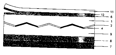
Example of one diffractive structure which can be prepared according to the
present invention
is given in Fig. 3 ( including processing) and an example of one possible
multilayer hologram
is presented in Fig. 9, where 6 stands for protecting layer which protects a
high refraction
index layer 2 or bearing layer 1 against environmental effect or against
undesirable effect or
CA 02323474 2000-09-11
11
consecutive exposure by UV light and improves resistivity of the final
product, 7 stands for
adhesive layer which enables either unrepeatable or repeatable anchoring of
the hologram or
other diffractive element on the protected article, 8 stands for fragile layer
which ensures
good adherence of two layers to each other and which depreciates itself during
any attempt
to peel off and thus causes irreversible deformation and destruction of the
diffractive
element, 9 stands for the anchor layer, which is usually used to improve
adherence of
adhesive layer 7 to high refraction index layer 2 or to the bearing layer 1,
10 stands for
adhesive layer providing clutching of hologram to the carrier 11 before its
own application.
Industrial exploitation
The present invention is applicable for fabrication ; of transparent and
semitransparent
diffractive elements and more particularly to a transparent and
semitransparent type
holograms. Besides of technical applications (e.g. record of picture or
information) these
products can be used in such activities of human beings as advertisement,
security sector,
safety technique, protection of product originality, money counterfeit
protection etc.