Note: Descriptions are shown in the official language in which they were submitted.
CA 02323610 2002-07-10
1
CIRCUIT AND METHOD FOR ELIMINATING
SURFACE CURRENTS ON METALS
Background of the Invention
7. Field of the Invention
The field of the endeavor of the invention relates to ground planes for
antennas and in particular to a method of reducing surface currents induced
by the antenna on the ground plane. Related subject matter may be found in
U.S. Patent No. 6,262,495 and the priority document to which it refers: U.S.
60/079,953 filed March 30, 1998.
2. Description of the Prior Art
A ground plane is a common feature of most radio frequency and
microwave antennas. It is comprised of a conductive surface lying below the
antenna and often performs a useful function by direcfiing most of the
radiation
into one hemisphere in which the antenna is located. Frequently, the ground
plane is present by necessity rather than by intent as in the case of a metal-
skinned aircraft. For many types of antennas, the ground plane degrades
antenna performance andlor dictates the antenna design itself. The most
obvious constraint is that the tangent electric field on the conductive
surface
must be zero, so that electromagnetic waves experience a 180° phase
shift
on reflection. This often imposes a minimum height of about a quarter
wavelength on the antenna. Furthermore, RF surface currents can propagate
freely along the metal surface of the ground plane. These surface
CA 02323610 2000-09-14
WO 99/50929 PCT/US99/06884
2
currents result in lost power due to radiation from edges or other
discontinuities, and interference between nearby antennas on the aircraft. In
phased arrays, surface currents are particularly problematic, contributing to
coupling between antenna elements and causing blind angles.
What is needed is some type of method or design which provides a
metallic surface which forbids RF current propagation and reflects
electromagnetic waves with zero phase shift.
What is further needed is some type of method or apparatus whereby
surface currents on ground planes associated with antennas can be
o suppressed to provide more efficient antennas, reduce coupling between
elements in a phased array, and reduce interference between nearby
antennas on aircraft.
Further, what is needed is a reflector which lacks edge currents that
radiate power into the back hemisphere of the antenna.
~5 What is needed is also ground plane in which a non-shifted phase of
the reflected waves enable smaller antennas to be realized, since the
radiating elements can be located very near the surface of the ground plane
without being shorted out by it.
CA 02323610 2002-07-10
3
Brief Summary of the Invention
The invention relates to an apparatus for reducing electromagnetically
induced surface currents in a ground plane comprising a plurality of elements.
Each element is a resonant circuit. Each cf the elements is interconnected
with each other to form an array. Each resonant circuit has an exposed
surface. The corresponding plurality of exposed surfaces of the plurality of
elements define the ground plane.
Each of the elements electrically functions as an LC resonant circuit.
Each of the elements has a subplurality of adjacent elements and is
capacitively coupled to each of the adjacent elements. Each of the plurality
of
elements is inductively coupled together in Common.
In the illustrated embodiment, the array of elements comprises a
corresponding plurality of separate conductive patches forming a surface. A
common conductive back plane is separated by a predetermined distance
from the surface of the patches. The plurality of patches form a common
surface. Each of the plurality of patches is coupled by a conductive line to
the
separated back plane. The apparatus further comprises a dielectric material
disposed between the back plane and the surface defined by the plurality of
elements.
In the illustrated embodiment, the dielectric material is a dielectric
sheet. The plurality of patches are conductive patches formed on a first
surface of the dielectric sheet and the back plane is a continuous conductive
surface disposed on an opposing surface of the dielectric sheet. The lines
connecting the patches to the back plane are metalizations formed in vias
defined through the dielectric sheet. The patches are hexagonal metalizations
defined on the first surface of the dielectric sheet.
The plurality of resonant elements are parameterized to substantially
block surface current propagation in the apparatus within a predetermined
CA 02323610 2000-09-14
WO 99/50929 PCT/US99/06884
frequency band gap. In particular, the plurality of elements are
parameterized to reflect electromagnetic radiation from the apparatus with a
zero phase shift at a frequency within a frequency band gap.
The apparatus further comprises an antenna disposed above or inside
the surface of resonant elements. In particular the antenna is comprised of a
radiative element disposed parallel to the surface of the resonant elements,
which act as a ground plane for the antenna.
In one embodiment the antenna is a wire antenna. In another
embodiment the antenna is a patch antenna. The patch antenna may be
substituted in position for one or more of the resonant elements and is
disposed in the surface of the resonant elements.
In another embodiment the plurality of elements comprise at least a
first and second set of elements. The first set of elements are disposed in a
first defined plane which comprises the ground plane. The second set of
~5 elements is disposed in a second defined plane. The second defined plane is
disposed above and spaced apart from the first ground plane. The arrays
formed by the first and second sets of elements each form an overlapping
mosaic, wherein each element of the second set overlaps and is spaced apart
from at least one of the elements in the first set of elements. In other words
2o the basic ground plane array has superimposed over it patches which are
also connected to the back plane, but which form a second plane of metallic
patches over the first plane of metallic patches.
In still another embodiment, the first and second set of elements each
comprise in turn one or more corresponding subsets of elements. Each
25 subset of the first set of elements are stacked over each other and each
subset of the second set of elements are stacked over each other. The
subset of the first set of elements are spaced apart from and adjacent to at
least one subset of the second elements, so that two or more layers of
CA 02323610 2004-02-06
alternating overlapping arrays of the first and second set of elements is
provided. In other words, the double layered ground plane discussed above
can be replicated an arbitrary number of times by vertically disposing
alternating layers of the overlapping patches to form tiers of patches. The
5 planes of patches can be added singly to comprise an odd number of planes
or pairwise to provide an even number of planes.
A dielectric material can be disposed between each plane of patches
and may either be the same type of dielectric material between each layer or
the material may be selectively chosen to provide a graded plurality of layers
of different types of dielectric materials.
In accordance with one aspect of the invention, there is provided a
method of reducing surface currents in a conductive surface comprising the
steps of providing the surface with a two dimensional array of a plurality of
resonant elements. Each resonant element is coupled with each other and
parameterized by geometry and materials to collectively exhibit a frequency
band gap in which surface propagation is substantially reduced.
Electromagnetic energy is radiated from a source disposed above the surface
of resonant elements at a frequency within the frequency band gap so that
electromagnetic radiation reflected from the surface has a zero phase shift at
a frequency within the frequency band gap.
The surface which is provided is a plurality of conductive elements
forming a periodic or nearly periodic array. Each element of the array has a
subplurality of adjacent elements to which it is capacitively coupled. Each of
the plurality of elements is inductively coupled in common with each other. In
particular, the resonant array of elements which is provided is a plurality of
conductive patches defining the periodic or nearly periodic array on a first
surface and a continuous conductive second surface separated by a
predetermined distance from the first surface. Each of the conductive patches
of the first surface is inductively coupled to the continuous conductive
second
surface.
The step of radiating electromagnetic energy from a source may
comprise radiating electromagnetic energy from an antenna disposed parallel
CA 02323610 2004-02-06
6
and adjacent to the surface of the array of elements, or radiating
electromagnetic energy from an antenna disposed in the surface of the array
of resonant elements.
In accordance with another aspect of the invention, there is provided
an apparatus for reducing electromagnetically induced surface currents at a
frequency having a free space wavelength, ~,, and in a ground plane
comprising a plurality of distributed elements collectively forming a periodic
two-dimensional mesh with a periodicity, a, each distributed element being a
distributed resonant circuit, each of the distributed elements being
interconnected with each other to form an array and each distributed resonant
circuit having a surface disposed in a defined plane, wherein each distributed
element is substantially equally electromagnetically coupled to each adjacent
distributed element, regardless of location within the array, and regardless
of
the direction of the element-to-element orientation within the array, the
corresponding plurality of surfaces of the plurality of elements defining the
ground plane, and wherein the periodicity of the elements is much less than
the free space wavelength (a«~,).
In accordance with another aspect of the invention, there is provided a
method of reducing surface currents in a conductive ground plane comprising
providing the conductive surface with a two dimensional array of a plurality
of
resonant distributed elements, each resonant distributed element being coupled
with each other and parameterized by geometry and materials to collectively
exhibit a frequency band gap in which surface propagation is substantially
reduced, regardless of the direction of the surface propagation in the two-
dimensional array, and wherein each distributed element is substantially
equally
electromagnetically coupled to each adjacent distributed element, regardless
of
location within the array, and regardless of the direction of the element-to-
element orientation within the array, and radiating electromagnetic energy
from
a source disposed above the surface of resonant distributed elements at a
frequency within the frequency band gap so that electromagnetic radiation
reflected from the surface has a zero phase shift at a frequency within the
frequency band gap.
CA 02323610 2004-02-06
6a
In accordance with another aspect of the invention, there is provided
an apparatus comprising a conductive back plane, a first set of conductive
patches aligned in a first plane with at least some of the first set of
patches
electrically connected to the back plane, and a second set of conductive
patches aligned in a second plane between the first plane and the conductive
back plane such that at least a portion of each conductive patch of the second
set is positioned between the conductive back plane and at least a portion of
at least one conductive patch of the first set with at least some of the
second
set of patches electrically connected to the back plane, the first set of
conductive patches and the second set of conductive patches forming a
plurality of distributed resonant elements.
In accordance with another aspect of the invention, there is provided a
ground plane mesh comprising a metallic back plane, a set of symmetrically
shaped metallic patches aligned in a first plane, the set of metallic patches
including any number of connected patches connected to the metallic back
plane through patch vias attached to centers of the any number of connected
patches, and a set of symmetrically shaped metallic plates aligned in a
second plane between the first plane and the metallic back plane such that at
least a portion of each metallic plate is positioned between the metallic back
plane and at least a portion of at least one metallic patch, the set of
metallic
plates including any number of connected plates connected to the metallic
back plane through plate vias attached to centers of the connected plates.
In accordance with another aspect of the invention, there is provided
an antenna comprising a radiative element aligned in an antenna plane, a
high impedance ground plane meshing including a plurality of distributed
resonant elements formed by conductive interconnected grounded patches
positioned within at least two planes substantially parallel to the antenna
plane.
In accordance with another aspect of the invention, there is provided
an apparatus comprising a conductive back plane, a plurality of conductive
patches forming a plurality of distributed resonant elements connected to the
CA 02323610 2004-02-06
6b
back plane and aligned within at least two planes substantially parallel to
the
conductive back plane, the patches positioned such that portions of patches in
one of the at least two planes are positioned between the conductive back
plane and at least a portion of at least one patch in another plane of the at
least two planes.
In accordance with another aspect of the invention, there is provided
an apparatus comprising a conductive back plane in a first plane, a plurality
of
conductive patches connected to the back plane and aligned in a second
plane and having a geometry arranged and configured to define a means with
a surface wave intensity frequency response across the apparatus having a
bandgap at frequencies greater than a lower frequency of an Ultra High
Frequency (UHF) range.
In accordance with another aspect of the invention, there is provided
an apparatus comprising a conductive back plane in a first plane, a plurality
of
conductive patches connected to the back plane and aligned in a second
plane and having a geometry arranged and configured to define a means for
suppressing surface currents in a surface defined by the conductive patches
at frequencies greater than a lower frequency of an Ultra High Frequency
(UHF) range.
The invention can be better visualized by now turning to the following
drawings wherein like elements are referenced by like numerals.
Brief Description of the Drawings
Fig. 1 is a circuit diagram equivalent of the ground plane mesh of the
invention showing the ground plane metal sheet covered by a thin two
dimensional layer of protruding elements, which are capacitively connected to
each other and inductively connected to the back metal surface. The
periodicity, a, of the metal elements on the opposing surface and the
thickness, t, of the ground plane mesh are much smaller than the free space
wavelength.
CA 02323610 2004-02-06
6c
Fig. 2(a) is the side cross-sectional view of the ground plane mesh 24
of the invention.
Fig. 2(b) is a top plan view of an actual finro dimensional capacitive of
ground plane structure of the ground plane mesh of the invention
incorporating the distributed inductance and capacitance of Fig. 1 (a).
Fig. 3(a) is a diagram illustrating a technique for measuring surface
waves modes on a ground plane mesh. The illustrated embodiment shows a
CA 02323610 2000-09-14
WO 99/50929 PCT/US99/06884
7
vertical monopole antenna probe, which transmits surface waves across the
ground plane, and a similar antenna for receiving the surtace waves.
Fig. 3b is a diagram illustrating another technique for measuring
surface waves across a ground plane mesh using monopole antenna probes
which are horizontally oriented.
Fig. 3c is a diagram illustrating a technique for measuring the reflection
phase of the ground plane mesh. Plane waves are transmitted from a horn
antenna, reflected by the ground plane, and received by a second horn
antenna.
Fig. 4(a) is a graph of the transmission intensity versus frequency
using the surface wave measurement technique shown in Fig. 3a. The band
edge is shown at about 28 GHz. Above that frequency, surface currents do
not propagate.
Fig. 4(b) is a graph of the transmission versus frequency for a
~5 conventional continuous metal sheet acting as a ground plane.
Fig. 5(a) is the polar radiation pattern of a monopole antenna mounted
on the ground plane mesh of the invention operating below the band edge at
a frequency of 26.5 GHz. The pattern shows many lobes and significant
radiation to the back hemisphere due to surface currents.
2o Fig. 5(b) is a polar radiation pattern of the same monopole shown in
Fig. 5(a) operating at a frequency of 35.4 GHz. The radiation of the back
hemisphere is reduced by 30 dB and the pattern shows no blind angles
associated with multi-path currents on the ground plane and exhibits only
smooth main lobes.
CA 02323610 2000-09-14
WO 99/50929 PCT/US99/06884
8
Fig. 5(c} is a polar radiation pattern of a similar monopole under
ordinary metal ground plane at 26.5 GHz.
Fig. 5(d) shows the polar radiation pattern of the monopole of Fig. 5(c)
at 35.4 GHz.
Fig. 6 is a graph showing the phase of the reflected waves measured
with respect to an ordinary metal surface of the ground plane mesh of the
present invention as a function of frequency. It is depicted that the phase
changes with the frequency and passes through a zero at about 35 GHz.
Fig. 7(a) is a graph of the surface wave transmission intensity as a
1o function of frequency over the ground plane mesh of the invention. The band
gap is clearly visible covering a range of 11 GHz to 17 GHz.
Fig. 7(b) is a graph of the phase shift of waves reflected from the
ground plane mesh of the invention shown as a function of frequency. Within
the band gap, waves are reflected in phase. Outside the band gap, waves
~5 are reflected out of phase as with ordinary continuous metal ground plane
sheets.
Fig. 8(a} is a diagrammatic depiction of a horizontal wire antenna lying
flat against a metal surface. This antenna will not radiate well due to
destructive interference from the waves that are reflected from the metal
2o surface since it is effectively shorted out by the metal surface or a
canceling
image formed in it.
Fig. 8(b) is a diagrammatic cross-sectional depiction of the same
horizontal wire antenna using the ground plane mesh of the invention. Due to
the favorable phase shift properties of the ground plane mesh, the antenna of
25 Fig. 8(b) is not shorted out and radiates well.
CA 02323610 2000-09-14
WO 99/50929 PCT/US99106884
9
Fig. 9(a) is a graph of the transmission as a function of frequency
showing the S11 return loss for the horizontal wire antenna above the metal
ground plane of Fig. 8(a). Return loss is more than minus 3 dB (50%)
indicating that the antenna rotates poorly.
Fig. 9(b) is the S11 return Toss from the same antenna above the
ground plane mesh of the invention as shown in Fig. 8(b). Below the tower
band edge, the antenna performs similarly to the antenna on the ordinary
ground plane sheet. Above the band edge, the return loss is around -10 dB
(10%) indicating good antenna pertormance.
Fig. 10{a) is the polar radiation graph of the antenna pattern for the
horizontal wire antenna of Fig. 8(a).
Fig. 10(b) is the polar radiation pattern of the horizontal antenna of
Fig. 8(b). The radiation level is about 8 dB more than on the metal ground
plane in Fig. 10(a) indicating much better antenna performance.
~5 Fig. 11(a) is a diagrammatic cross-section depiction of a patch antenna
above the conventional continuous metal ground plane.
Fig. 11 (b) is a diagrammatic side cross-sectional view of the same
patch antenna of Fig. 11 (a) but incorporated into the ground plane mesh of
the invention.
2o Fig. 12 is the S11 measurement of both patch antennas of Figs. 11(a)
and 11 (b) indicating that they have similar return loss and similar radiation
band widths. The antenna of Fig. 11 (a) is shown in dotted outline while the
antenna of Fig. 11 (b) is shown in solid outline.
Fig. 13(a) is a polar radiation pattern of the conventional patch antenna
25 of Fig. 11 (a). The pattern shows significant radiation of the backward
CA 02323610 2000-09-14
WO 99/50929 PCT/US99/06884
l0
hemisphere and the radiation pattern of the forward hemisphere is
characterized by ripples. Both of these effects are caused by surtace
currents on the conventional metal ground plane. The E plane graph is
shown in solid outline and the H plane graph in dotted.
Fig. 13(b) is the polar radiation pattern of the patch antenna of
Fig. 11 (b). This antenna has less backward radiation than the antenna of
Fig. 11 (a). The pattern is much more symmetrical and does not have ripples
in the front hemisphere. These improvements are due to the suppression of
surface currents by the ground plane mesh.
Fig. 14(a) is the side cross-sectional view of an alternate embodiment
of the ground plane mesh in which the top metal patches form two
overlapping layers, separated by a thin dielectric spacer. This increases the
capacitance between adjacent elements, lowering the frequency.
Fig. 14(b) is a top plan view of the structure shown in Fig. 14a. The
15 top layer of metal patches are shown overlapping the second layer below.
Fig. 15(a) is a graph of the surface wave transmission intensity versus
frequency on the structure depicted in Fig. 14(a) and Fig. 14(b). The band
gap can be seen to cover the frequency range of 2.2 GHz to 2.5 GHz.
Fig. 15(b) is a graph of the reflection phase of the structure depicted in
2o Fig. 14(a) and Fig. 14(b). The reflection phase crosses through zero at a
frequency within the band gap.
The invention can be better understood by considering the illustrated
embodiments are set forth in the following detailed description. The
illustrated embodiments provided by example only and it is not intended to
25 limit the invention which is defined by the following claims.
CA 02323610 2000-09-14
WO 99!50929 PCT/US99/06884
Detailed Description of the Preferred Embodiments
A two dimensional periodic pattern of capacitive and inductive
elements defined in the surtace of a metal sheet are provided by a plurality
of
conductive patches each connected to a conductive back plane sheet
between which an insulating dielectric is disposed. The elements acts to
suppress surface currents in the surface defined by them. In particular, the
array forms a ground plane mesh for use in combination with an antenna.
The performance of a ground plane mesh is characterized by a frequency
o band within which no substantial surface currents are able to propagate
along
the ground plane mesh. Use of such a ground plane in aircraft or other
metallic vehicles thereby prevents radiation from the antenna from
propagating across the metallic skin of the aircraft or vehicle. This
eliminates
surface currents on the ground plane thereby reducing power loss and
~5 unwanted coupling between neighboring antennae.
The invention is comprised of the continuous metal sheet 30 spaced
apart from and covered with a thin, two-dimensional pattern of protruding
metal elements 10 schematically denoted in Fig. 1 by dotted box 10. Each
element 10 is capacitively coupled to its neighbors and inductively coupled to
2o the metal sheet. Turn, for example, to the schematic diagram of Fig. 1 in
which elements 10 are schematically shown as being capacitively coupled to
each other by virtual capacitors 12 and inductively coupled to the sheet 30 by
virtual inductors 14. Elements 10 are provided in the form of a thin mesh
which thus acts as a two dimensional network of parallel resonant circuits,
25 which dramatically alter the surface impedance of mesh 24 collectively
comprised of the array of elements 10.
CA 02323610 2000-09-14
WO 99/50929 PCT/US99/06884
12
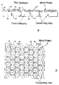
Turn now to the schematic diagrams of Fig. 2(a). Fig. 2(a) is a side
cross-sectional view of a printed circuit board in diagrammatic form. Circuit
board 24 is made of conventional insulating material 26. The back surface 28
of board 24 is provided with a continuous metal sheet 30, such as a sheet of
copper cladding. Front surface 32 of board 24 is patterned with a two
dimensional triangular lattice of hexagonal metal patches 34 each of which is
coupled to rear plate 30 by means of a metal via connector 36. Clearly, the
dimensions can be arbitrarily varied according to the application in a manner
consistent with the teachings of the invention.
In effect, circuit board 24 is a two dimensional frequency filter
preventing RF currents from running along metal surface 30. Even though
patches 34 are arranged in a triangular lattice, it must be understood that
the
invention is not limited to this geometry nor need it be exactly periodic. The
more important parameters are the inductance and capacitance of the
~5 individual elements on the surface. Hence, it must be explicitly understood
that many other geometries and non-periodic patterns may be employed
consistent with the teachings of the inventions with respect to the inductance
and capacitance of each element.
Fig. 2(b) is a top plan view of ground plane mesh 24 of Fig. 2(a) .
2o Each element 34 is provided in the form of hexagon connected at its center
with metal via 36. Hexagonal elements 34 form a triangular lattice across the
surface of mesh 24.
Consider now the operation of ground plane mesh 24 when a wave is
launched at one end of its surface using either a monopole antenna probe
25 and received with a similar antenna at its opposing end as diagrammatically
shown in the top plan view of Figs. 3a and 3b for vertical and horizontal
CA 02323610 2000-09-14
WO 99/50929 PCT/US99/06884
13
monopole antennas respectively. A strong transmission indicates coupling to
a surface mode in ground plane mesh 24.
Fig. 4(a) is a graph showing the transmission amplitude in dBs as a
function of frequency in GHz measured in the test configuration of Fig. 3(a).
Lower band edge 54 is clearly shown in the experimental results depicted in
4(a) at about 28 GHz where the transmission amplitude drops sharply by 30
dB. Above the lower band edge 54, the surface currents are blocked by the
pattern of parallel resonant circuits on the top surtace of ground plane mesh
24. The upper band edge cannot be seen in the depiction of Fig. 4(a) since
the measurement apparatus was limited to 50 GHz in its range.
Compare the transmission performance of the invention of Fig. 4(a)
with that of a conventional plane metal sheet as shown in Fig. 4(b). Within
the band gap, namely, the frequency range between the lower and upper
band edges, transmission across the structure of the invention is 20 dB less
than over ordinary metal sheet. Thus, a comparison of Figs. 4(a) and (b)
provide valid evidence for the suppression of surface current propagation in
the ground plane mesh 24 of the invention.
Consider now the effects of ground plane mesh 24 on a small
monopole antenna. In this test a coaxial cable is inserted through the rear
2o side of ground plane mesh 24 with the center pin of the coaxial cable
extending 2 mm beyond the front side of ground plane mesh 24 to thus serve
as a monopole antenna. The outer conductor of the coaxial cable was
connected to the continuous metal backside sheet 30 on the rear side of
ground plane mesh 24. The antenna pattern as measured in an anechoic
chamber as a function of angle is shown Figs. 5(a) and 5(b) which are polar
plots of the antenna pattern below and above the band edge, respectively.
Below the band edge as shown in Fig. 5(a) the monopole antenna radiates in
CA 02323610 2000-09-14
WO 99/50929 PCT/US99/06884
14
ail directions including into the back hemisphere between 90° and
270°. The
polar pattern shows the azimuthal distribution of the antenna gain with the
radial distance from the center of the graph being the transmission intensity
in
dB. The front hemisphere would thus be the angles between 90° and
270°
through 0° which would be the forward direction. The back hemisphere is
between 90° and 270° through 180° which would be the rear
facing direction.
The backward radiation of Fig. 5(a) is due to currents that propagate
along the ground plane and radiate power from the edges. The pattern also
contains many lobes due to surtace currents forming standing waves on the
ground plane. Above the band edge, the back plane currents are eliminated
as dramatically shown in Fig. 5(b). The resulting antenna pattern is smooth
and antenna rejection in the rear hemisphere is greater than 30 dB. Since the
surtace currents cannot propagate to the edges, the finite size and capacity
of
ground plane that was actually used appears as it if were infinite.
15 For comparison purposes, the same polar plots are shown in Figs. 5(c)
and 5(d) at the same frequencies but for a conventional metal ground plane
or solid metal sheet. As expected, Fig. 5(c) and Fig. 5(d) both show many
lobes and significant radiation into the back hemisphere.
Several conclusions can be drawn from the measurements described
2o above. First, radio frequency surtace currents are often present in a real
antenna environment and they have a significant impact on the antenna
radiation pattern. The ground plane mesh 24 of the invention substantially
reduces RF surtace wave propagation and achieves a corresponding
improvement in the antenna pattern. Although the demonstration above
25 involved a simple monopole, the results suggest that improvement of the
invention is realized in many types of antennas. Ground plane mesh 24 of
the invention can improve the efficiency of patch antennas which tend to lose
CA 02323610 2000-09-14
WO 99/50929 PCT/US99/06884
IS
significant power to surface waves. In phased arrays, the structure of the
invention can reduce blind angle effects and coupling between elements. On
aircraft, interference between nearby antennas can be reduced by using
guard rings having the two dimensional geometry of the ground plane
structure of the invention. In wireless telephony a surtace devised according
to the invention could be used to direct electromagnetic radiation away from
the user. Most importantly, antenna designs that were previously impractical
because of the deficiencies of a conventional metal ground plane now
become feasible with the ground plane mesh 24.
A second important property of the invention is that it reflects an
electromagnetic wave with a different phase than ordinary metal surfaces.
The phase of reflection can be tested by launching a plane wave toward the
surface using a horn antenna, and measuring the phase of the wave
received by a second horn antenna. The phase of the reflected wave is
~ 5 shown in Fig. 6. Below the band gap at 28 GHz, the phase of the reflected
wave is the same as with an ordinary metal surtace indicating a phase shift of
180° on reflection. Near the band edge, at 28 GHz, the phase shift
passes
through the value 90° while at 35 GHz the reflected wave has a zero
phase
shift. A ground plane with a zero phase shift would not have an electric field
2o node at its surface, but rather an antinode. The antenna could then be
placed very near the surface of ground plane mesh 24 without being shorted
out.
A phase shift that varies with the frequency near the band edge at 28
GHz can be associated with an equivalent time group delay. It is natural to
25 discuss what thickness of dielectric would be associated with the group
delay
of the monopole antenna illustrated in Figs. 5(a) and (b). The equivalent
thickness, considering the dielectric constant of material 26 at e=2.2, is
equal
CA 02323610 2000-09-14
WO 99/50929 PGT/US99/06884
16
to three times the actual thickness of ground plane mesh 24. .Thus, the phase
shift is not simply due to the thickness of ground plane mesh 24, but rather
is
an energy storage affect of the resonant circuit on the surtace of ground
plane
mesh 24. Alternatively, it can be viewed as an enhanced effective dielectric
constant due to the resonant nature of the material.
The invention can be used to improve the properties of antennas such
as the simple monopole antenna by replacing the conventional metal ground
plane with ground plane mesh 24. Elimination of radiation in the back
hemisphere and smoothing of the antenna pattern can be expected from
monopole antennas and antennas of other designs. By increasing the
capacitance and inductance, it must be understood that structures fabricated
according to the teachings of the present invention can operate not only at
the microwave frequencies discussed in connection with the illustrated
embodiment, but also operated at ultra high frequencies (UHF) or lower.
~5 By increasing the capacitance and inductance in the parallel resonant
circuits comprising ground plane mesh 24, the frequency of the lower band
edge can be reduced. The surface current transmission across the structure
is shown in Fig. 7(a) in which the band gap is clearly visible between 11 and
17 GHz. Fig. 7(b) shows the phase shift that occurs for electromagnetic
2o waves that are reflected from a surface provided with this capacitance and
inductance. At low frequencies, the reflection phase is 180° indicating
the
reflected wave is out of phase with the incident wave. In this low frequency
range, the surface thus resembles an ordinary continuous metal ground plane
sheet. As the frequency is increased beyond the lower band edge 54, the
25 waves are reflected in phase. Within the band gap shown in shaded zone in
the right portion of Fig. 7(b) the waves are reflected in phase. Thus within
the
band gap an antenna placed near such a structure would experience
CA 02323610 2000-09-14
WO 99/50929 PCTNS99/06884
17
constructive interference from the reflected waves and would not be shorted
out. The phase of the reflection crosses zero within the band gap and
eventually approaches -180° for frequencies beyond the upper band edge
56.
Ground plane mesh 24 of the invention thus allows the production of
low profile antennas which were not possible on ordinary metal ground
planes. Fig. 8(a) shows a prior art horizontal wire antenna 48 lying flat
against or spaced slightly above a conventional metal ground plane 60 as
might occur in the skin of the aircraft. Fig. 8(b) shows the same antenna 58
disposed above a ground plane mesh 24 of the invention. The S11 return
loss of the antenna of Fig. 8(a) is shown in the graph of 9(a) wherein
transmission is graphed against frequency. The S11 return loss is a
measurement of the power reflected from the antenna back toward the
source. This antenna reflects more than -3 dB or 50% of the power back into
the microwave source thus providing a very poor radiation performance. Poor
~5 radiation performance understandably arises because of the unfavorable
phase shift of the metal surtace of ground plane 60 which causes destructive
interference with the direct radiation from antenna 58 and the radiation
reflected from metal surface 60.
Fig. 9(b) shows the S11 return loss of the same antenna 58 with
2o ground plane mesh 24. Below the band edge 54 antenna 58 also pertorms
poorly resembling configuration of the antenna above a conventional metal
ground plane shown in Figs. 8(a) and 9(a). Above band edge 54,
electromagnetic waves are reflected from the surface of ground plane mesh
24 in-phase thus reinforcing the direct radiation. Antenna 58 performs well
25 with a return loss of about -10 dB (10%).
The polar radiation patterns of antenna 58 in the two ground plane
configurations of Figs. 8(a) and 8(b) are shown in Figs. 10(a) and 10(b),
CA 02323610 2000-09-14
WO 99/50929 PCT/US99/06884
18
respectively. Measurements were taken at 13 GHz and plotted on the same
scale. Wire antenna 58 on ground plane mesh 24 has about 8 dB more gain
than on the conventional metal ground plane thus agreeing with the S11
measurement.
Similarly, Figs. 11 (a) and 11 (b) are side cross-sections of diagrammatic
depictions of patch antennas 62 mounted in Fig. 11 (a) above an ordinary
metal ground plane surtace 60 and in Fig. 11 (b) above ground plane mesh
24. The antenna return loss measured for the antenna configurations of
Figs. 11 (a) and 11 (b) are shown in the graph of Fig. 12. Both configurations
have similar return losses and bandwidths. Fig. 13(a) shows polar radiation
pattern of patch antenna 62 on metal surface 60 at 13.5 GHz where the return
loss of both antennas is equal. The pattern has significant radiation in the
backward hemisphere as well as ripples in the forward hemisphere. Both of
these effects are caused by surface currents on the ground plane.
Fig. 13(b) shows a polar radiation pattern for patch antenna 62 with
ground plane mesh 24. The pattern is smoother and more symmetric and
has less radiation in the backward direction. The antenna also has about 2
dB more gain more than when used with conventional ground plane.
Fig. 14(a) is the side cross-sectional view of an alternate embodiment
20 of ground plane mesh 24 in which the top metal patches 62 are disposed
above and overlapping plates 34 in mesh 24 and separated from plates 34 by
a thin dielectric spacer 70 . Fig. 14(b) is a top plan view of the structure
shown in Fig. 14{a). The top layer of metal patches are shown overlapping
the second layer below. This increases the capacitance between adjacent
25 elements, thereby lowering the frequency. Conducting vias 72 connect some
or all of metal patches 62 to a solid metal sheet 30, which is separated from
the multiple layers of metal patches 62 and plates 34 by a second dielectric
CA 02323610 2000-09-14
WO 99/50929 PCT/US99/06884
19
layer 26. Additional layers of metal patches 62 and dielectric~sheets 70 can
be vertically added in addition to that shown in Fig. 14(a) as desired to
realize
a desired capacitance.
The electromagnetic characteristics of the ground plane mesh 24 of
Figs. 14(a) and 14(b) is depicted in the graphs of Figs. 15(a) and 15(b). Fig.
15(a) is a graph of the surface wave transmission intensity versus frequency
on the structure depicted in Figs. 14 (a) and 14(b). The band gap can be
seen to cover the frequency range of 2.2 GHz to 2.5 GHz. Fig. 15(b) is a
graph of the reflection phase of the structure depicted in Figs. 14(a) and
14(b). The reflection phase crosses through zero at a frequency within the
band gap.
Thus, it can be understood that the frequency of operation of ground
plane mesh 24 can be tuned by adjusting the geometry. Low profile antennas
on ground plane mesh 24 demonstratively perform better than similar
~5 antennas on solid metal ground planes. While the illustrated embodiment has
shown only comparative use of a vertical monopole or horizontal wire and a
patch antenna, other antenna designs could be employed in a similar manner.
Both antenna configurations take advantage of the surface wave suppression,
while the horizontal wire antenna benefits from the reflection of phase
2o property of the surface of ground plane mesh 24 more than a patch antenna
and provides thus a new antenna geometry that would not otherwise be
possible.
In summary, it can be now realized that ground plane mesh 24 of the
invention:
25 (1) is comprised of a metal ground plane incorporating a thin two
dimensional arrangement of metal elements;
CA 02323610 2000-09-14
WO 99/50929 PCT/US99/06884
(2) each element is capacitively coupled to nearby-elements and
inductively coupled to the ground plane of the back sheet 30;
(3) mesh 24 forms a two dimensional network of parallel resonant
circuits;
5 (4) parallel resonant circuits block surface current propagation on
ground plane mesh 24; and
(5) the resonant nature of ground plane mesh 24 alters the phase
electromagnetic waves that are reflected from its surface.
Ground plane mesh 24 blocks the propagation of RF electric currents
along its surface.
Many alterations and modifications may be made by those having
ordinary skill in the art without departing from the spirit and scope of the
invention. Therefore, it must be understood that the illustrated embodiment
has been set forth only for the purposes of example and that it should not be
~5 taken as limiting the invention as defined by the following claims.
The words used in this specification to describe the invention and its
various embodiments are to be understood not only in the sense of their
commonly defined meanings, but to include by special definition in this
specification structure, material or acts beyond the scope of the commonly
2o defined meanings. Thus if an element can be understood in the context of
this specification as including more than one meaning, then its use in a claim
must be understood as being generic to ail possible meanings supported by
the specification and by the word itself.
The definitions of the words or elements of the following claims are,
therefore, defined in this specification to include not only the combination
of
elements which are literally set forth, but all equivalent structure, material
or
CA 02323610 2000-09-14
WO 99/50929 PCT/US99/06884
21
acts for performing substantially the same function in substantially the same
way to obtain substantially the same result. In this sense it is therefore
contemplated that an equivalent substitution of two or more elements may be
made for any one of the elements in the claims below or that a single element
may be substituted for two or more elements in a claim.
Insubstantial changes from the claimed subject matter as viewed by a
person with ordinary skill in the art, now known or later devised, are
expressly
contemplated as being equivalently within the scope of the claims. Therefore,
obvious substitutions now or later known to one with ordinary skill in the art
1o are defined to be within the scope of the defined elements.
The claims are thus to be understood to include what is specifically
illustrated and described above, what is conceptionally equivalent, what can
be obviously substituted and also what essentially incorporates the essential
idea of the invention.