Note: Descriptions are shown in the official language in which they were submitted.
CA 02323644 2000-10-18
Connector having shuntable and configurable
contacts.
The present invention relates to a connector having
s shuntable and configurable contacts. More particularly,
the invention finds use in the field of "shunt"
connectors, to allow connectors to selectively
interconnect fixed tracks of a printed board integrated
in the connector. These connectors have contacts, for
io instance connected to individual tracks of a printed
board, which contacts may be selectively connected with
each other to provide connection between fixed tracks.
The invention particularly is particularly suitable for
connectors used in aeronautic applications, particularly
is on aircraft engines. A connector according to the
invention has the advantage that it can be used in
difficult external conditions, particularly at high
temperature (of the order of 150°C).
In prior art, connectors are known which have
Zo contacts, typically fitted on printed boards. A printed
board has fixed tracks typically engraved in a board
substrate. In order to connect two tracks together when
desired, if the pattern of the printed board does not
allow to do so, each track has to be provided, at a
2s desired point, with a contact and connection has to be
ensured between these contacts. For instance, a prior
art connector is known which has such contacts that
first ends of these contacts may, for example, be in
contact each with a track of the printed board, and that
3o second ends of these contacts are free on a rear surface
of the connector.
CA 02323644 2000-10-18
2
In prior art, two free ends of contacts disposed
within the same connector are interconnected, shorted,
by usi ng a conducti ve el ement to be put i n contact wi th
the two contacts. Particularly, in document EP-A-0 576
s 365, a connector is known which has conductors, so that
each conductor may be put in contact with another by
means of a u-shaped bar. u-shaped bars are typically
disposed in a cover to be fitted on the connector.
Depending on the arrangement of the bars, short circuits
io between conductors can be obtained or prevented. Hence,
the number of covers to be provi ded shal l correspond to
the possible combinations of connections between
conductors. Each cover provides a specific lay-out of u-
shaped bars.
is From the principle of document EP-A-0 576 365,
covers are also known which have conductive elements, so
that these conductive elements are put or not in contact
with each other, as a function of the height of a wall
separating two adjacent conductive elements. zn this
2o document, the provided configuration of short circuits
is defined by the respective heights of the cover walls.
Hence, the number of covers to be provided, with
different wall height arrangements shall correspond to
the possible combinations of connections between
Zs conductors.
This solution involves a problem. while it has an
easy implementation, the different covers being easily
mounted, it involves at each new configuration, the
complex process of removing the cover, detaching the
3o conductive elements therefrom, disposing them in a new
appropriate cover, and fitting this new cover on the
connector. This solution involves many individual
elements, which may get lost during a configuration
change of the connector and of connections.
3s The invention has the object to obviate the above
problems by providing a connector which has configurable
contacts. The solution proposed by the invention
CA 02323644 2000-10-18
3
provides a connector which has conductive means for
shorting the different contacts together. The interest
of the invention lies in that it provides a system which
allows to displace these conductive means between a
s first position in which they are in contact, and a
second position in which they are not in contact. To
this end, a connector according to the invention
includes power contacts having, at different heights, an
insulating surface and a conductive surface.
to Also, the connector includes contacts to be
powered, each provided with a sliding and conductive
socket to come or not into contact with an insulating
surface, or with a conductive surface of a power contact
of the connector. The invention also allows to connect a
is power contact with several contacts to be powered.
Further, a contact to be powered may be selectively put
in contact with a power contact independently of the
connections established between this power contact and
other contacts to be powered. This allows to change one
Zo connection only, without having to reestablish all the
others.
Furthermore, a connector according to the invention
may also be configurable to be adapted to different
types of complementary connectors. Depending on the
2s posi ti on of sockets al ong contact axes , a contact has a
more or less long contact end to be connected with a
complementary contact of a complementary connector. In
fact, the sliding socket is movable between a high
position and a low position. In the high position, it
3o completely hides the contact along which it slides. In
said high position, it is mechanically joined to the
insulating portion of the power contact. Thereby, the
contact is inaccessible to connection with a
complementary connector, and it is not powered.
3s Conversely, in the low position, the socket exposes a
free contact end . The free contact end may be connected
with a complementary connector. Also, in this low
CA 02323644 2000-10-18
4
position, the socket ensures connection with a
conductive portion of the power contact.
Finally, the shape of sockets is such as to allow
them to interlock mechanically with projections of the
s insulating or conductive surfaces of power contacts.
these interlocks help to retain the configurable
connections. The conductive and insulating surfaces of
power contacts may be obtained by crimping sleeves
thereon, i.e. plugging them in with a much higher force
io than by manual insertion.
Hence, the invention relates to a connector which
has a body, at 1 east one powe r contact and at 1 east one
contact to be powered, each of the contacts having a
fi rst end fi tted i n the body, characteri zed i n that the
is power contact has an insulating surface and a conductive
surface, and in that the contact to be powered has a
conductive socket, sliding along the contact to be
powered, between a first position in which the socket is
in contact with the insulating surface, and a second
2o position in which the socket ensures connection with the
conductive surface, so that the connection obtained in
the second position is conductive and allows powering of
the contact to be powered by the power contact.
The invention will be understood more clearly by
2s reading the following description and by analyzing the
accompanying figures. The latter are only shown by way
of example and do not intend to limit the invention in
any manner. The figures show:
- Figure 1: a sectional view of a first embodiment
30 of a connector according to the invention;
- Figure 2: a sectional view of a second embodiment
of a connector according to the invention;
- Figure 3: a top partial view of a connector
according to the invention;
3s - Fi gure 4: a top vi ew of a connector accordi ng to
the invention;
- Figure 5: a sectional view of an improvement of a
CA 02323644 2000-10-18
s
connector according to the invention;
- Figure 6: a top view in three different levels of
an embodiment of a connector according to the invention.
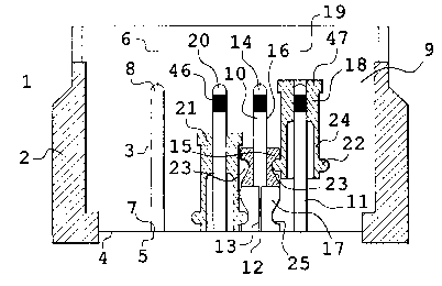
Figure 1 shows a connector 1 according to the
s invention. The connector 1 comprises a body 2, wherein
contacts are di sposed . A contact 3 i s mounted i n a rear
insulator 4 of the body 2. The rear insulator 4 has a
receiving hole 5 for accommodating the contact 3. As a
whole, the contact 3 has a shape elongating along an
io axis 6. The axis 6 is preferably orthogonal to a plane
formed by the rear insulator 4. The contact 3 has a
first end 7 and a second free end 8, the first end 7
bei ng i nserted i n the hol a 5 . The contact 3 i s di sposed
inside the body 2 so that a portion of the contact 3
is protrudes i n a cavi ty 9 of the body 2 . A depth of thi s
cavity 9 is preferably greater than a length of the
protruding portion of the contact 3. Therefore, the end
8 of the contact 3 does not project out of the body 2.
gy its end 7, the contact 3 may be connected to a track
Zo of a printed board, particularly by soldering.
The connector 1 comprises a power contact 10 and a
contact to be powered 11. The contacts 10 and 11 are of
the same type as the contact 3. The contact to be
powered 11 is situated in the proximity, in the
2s immediate vicinity of the power contact 10. Here,
immediate vicinity means that no contact is interposed
between two adjacent contacts. The power contact 10 is
fitted in a receiving hole 12 of the rear insulator 4.
The powe r contact 10 has an end 13 , 1 i ke the end 7 , and
3o an end 14, 1 i ke the end 8 . The end 13 i s fi tted i n the
hole 12. This end 13 is connected to a power source (not
shown) or to a track of a printed board (not shown)
whereon the connector is fitted.
The end 14 is free inside the cavity 9. In a
3s preferred embodiment of a connector according to the
invention, the power contact 10 is selectively
connected, or not, with one or more contacts to be
CA 02323644 2000-10-18
6
powered. For this purpose, the contact 10 has an
insulating surface 15. In a preferred embodiment of the
invention, the insulating surface 15 is obtained by
fitting an insulating sleeve around the power contact
s lO.
The insulating surface 15 is situated between the
ends 13 and 14, so that a first conductive surface 16
may be defined, in the upper portion, between the
i nsul ati ng surface 15 and the end 14, and that a second
io conductive surface 17 may be defined in the lower
portion between the insulating surface 15 and the end
13. In this preferred embodiment, the conductive surface
17 is obtained by fitting a sleeve around the power
contact 10. For instance, the conductive sleeve 17 may
is have a symmetrically inverted shape with respect to that
of the insulating sleeve 15. Then, the sleeves 15 and 17
are crimped around the power contact 10. They may
preferably be force-fitted around the contact.
Typically, the conductive sleeve 17 abuts against the
ao rear insulator 4. The respective positions of the
sleeves 15 and 17 may as well be inverted.
zn one variant, the free end 14 of the power
contact 10 may be arranged to be connected to a
complementary contact of a complementary connector.
2s The contact to be powered 11 has a socket 18
sliding along a protruding part of the contact to be
powered 11. The socket 18 slides along an axis 19 of the
contact to be powered 11, such as the axis 6. The
contact to be powered 11 is shown with the socket 18 in
3o the high position. Another contact to be powered 20,
like the contact to be powered 11, has a socket 21, like
the socket 18. The contact to be powered 20 is shown
with the socket 21 the low position.
The socket 18 may ensure conductive connection
3s between the contact to be powered 11 and the power
contact 10. zn a first embodiment, shown in figure 1,
the socket 18 is made of a conductive material ensuring,
CA 02323644 2000-10-18
7
on the one hand, electric connection with the contact to
be powered 11. The socket 18 i s mounted i n contact wi th
the contact to be powered 11. On the other hand, in
order to ensure conductive connection with the power.
s contact 10, the socket 18 has a projection 22 to come in
contact with the power contact 10. This projection 22
is, for instance, a shoulder on the periphery of the
socket 18.
Depending on the position of the socket 18 along
io the axis 19, the projection 22 rests against different
portions of the power contact 10. Particularly, in a
high position, the projection 22 rests against the
insulating surface 15 of the power contact 10. In a low
position, the projection 22 comes in contact with the
is conductive surface 17 of the power contact 10.
In the first embodiment, as shown in figure 1, the
insulating surface 15 is a cylindrical sleeve fitted
around the power contact 10. It particularly has an
undercut 23. This undercut 23 is adapted to receive and
2o retain the projection 22. In this embodiment, the
projection 22 is formed on a tongue 24 of the socket 18.
The latter may consist of a tube having at least two
slits. Thus, when the socket 18 passes from the high
posi ti on to the 1 ow posi ti on , the tongue 24 i s sl i ghtl y
2s deflected so that the projection 22 may slide along an
outer wall of the insulating sleeve 15. Then, when the
socket 18 reaches its low position, the projection 22 is
released and engages in the first undercut 23 or in the
second complementary undercut 25 of the conductive
3o sleeve 17. The projections might be inverted: they may
be provided in the sleeves of the power contact, whereas
undercuts may be provided in the socket of the contact
to be powered.
A second embodiment of a connector according to the
3s invention is shown in figure 2. A connector 100 has a
contact to be powered 111, surrounded by a socket 118 to
come into contact with a power contact 110. In this
CA 02323644 2000-10-18
8
embodiment, the socket 118 is made of an insulating
material.
In order to ensure conductive connection between
the contact to be powered 111 and the power contact 110,
s the socket 118 has a conductive blade 122. This
conductive blade 122 is fitted in the insulating body of
the socket 118 in such a manner that it has a first bend
27 to come into contact with the power contact 110,
particularly in undercuts thereof, and a second bend 28
to to come into contact with the contact to be powered 111.
As hereinbefore, in this embodiment the insulating
surface is an insulating sleeve 15 fitted around the
power contact 110. This sleeve 15 has a complementary
undercut for holding the bend 27 therein. A conductive
is surface i s adj acent to the i nsul ati ng su rface 15 , and
consists of a conductive sleeve 17. The bend 28 comes in
direct contact with the contact to be powered 111,
whereby it is in permanent contact therewith, whereas
the bend 27 is alternatively in contact with the
Zo insulating sleeve 15 or with the conductive sleeve 17.
As a variant, the sleeve 15 or 17 is conductive, but the
depth of the undercuts is such that it can push or not
the bend 28 against the contact to be powered 111.
connector cap may be also provided to protect the
Zs connector from dirt or short-circuit risks.
In one variant, there might be provided a power
contact 10 which is encircled, over a limited height
only, by a circular insulating layer which is situated
at half height between the two ends 13 and 14. zn such
3o an embodiment, a conductive connection ensured by a
socket surrounding a contact to be powered would be
achieved by direct contact with the power contact 10
whereas insulation would be achieved by contact with the
insulating layer. Nevertheless, in this case, no
3s mechanical restraint would be possible.
Typically, the connector 1 comprises several
contacts to be powered 11 arranged around several power
CA 02323644 2000-10-18
9
contacts 10. ,4 preferred embodiment of this type of
connector consists in minimizing the number of power
contacts 10 and maxi mi zi ng the number of contacts to be
powered 11. Hence, advantages are obtained from an
s optimized arrangement of contacts to be powered around
power contacts. Thus, a geometrical arrangement of
contacts to be powered 11 around power contacts 10 is
preferred. Particularly, in a preferred embodiment, a
set of contacts to be powered is disposed in such a
to manner that each contact to be powered is at the same
distance from the central power contact designed to
power said set of contacts to be powered. Further, in
order to minimize the space required by contacts to be
powered around the power contact, contacts to be powered
is are disposed equilaterally around said central power
contact.
In a prefe r red embodi ment , as shown i n fi gu re 3 , a
power contact 29, like the power contact 10, is
surrounded by six contacts to be powered 30 - 35, like
2o the contact to be powered 11. these contacts to be
powered 30 - 35 form a set 36. Each of these contacts to
be powered 30 - 35 is encircled by its respective socket
37 - 42.
If the sockets are of the same type as the ones of
2s figure 2, i.e. insulating sockets, these sockets 37 - 42
have a hexagonal section. Thus, a face 43 of a socket 38
comes to rest against a portion of the power contact 29.
Two faces 44 and 45, adjacent to the face 43 come
into contact with the adjacent faces of the sockets 37
3o and 39 respectively. The sockets of the set 36 have
identical shapes and are disposed in the same manner
relative to the contact of the power contact 29.
zn this embodiment a center distance between an
axis of a power contact and an axis of a contact to be
3s powered is of the order of 3 millimeters. Also, a
diameter of a power contact or of a contact to be
powered is of the order of 1 millimeter. A power contact
CA 02323644 2000-10-18
i s typi cal 1 y su r rounded by a maxi mum of si x contacts to
be powered . zn fact , i t i s di ffi cul t to provi de sockets
with a smaller inside diameter to come in contact with a
closer power contact.
s In this embodiment of a hexagonal socket, a
honeycomb arrangement of sockets, and of contacts, is
achieved. This arrangement allows the contacts to be
assembled together with no interstices therebetween.
Furthermore, if a stress is exerted on an edge of a
to contact, then the structure of the whole set of contacts
joined together remains unchanged. The hexagonal
arrangement of six contacts to be powered around a
central power contact ensures a high contact positioning
and retaining accuracy.
is In the variant, this arrangement also allows to
ensure a better exposure of contacts for connection with
a complementary connector.
The contacts disposed in the connector 1 according
to the i nventi on al so have a gui di ng mark 46, typi cal 1 y
2o situated in a portion of the contact in the proximity of
the free end, like the end 8. The power contact 10 also
has a guiding mark in this free portion. The interest in
providing such a mark 46 lies in that it allows to
visually identify powered contacts in a quick and easy
as manner. zn fact, when the socket 18 is in the high
position, the mark 46 is invisible, as it is hidden by
the socket. Conversely, when the socket 18 is in the low
position, the mark 46 is visible. this mark may be a
_.., .
3o Hence, a connector according to the invention may
be configured as desired. Each contact to be powered may
be set either in a powered state or in an non-powered
state relative to a power contact, with no effect of
this selection on powering of the adjacent contacts to
3s be powered, nor on poweri ng of contacts i n general . the
sockets of each contact to be powered are easily
disalaced in an individual and independent manner. Each
CA 02323644 2000-10-18
11
socket has a gripping area 47, allowing it to be
gri pped, for i nstance by hand, to move the sockets i nto
a selected position. In one preferred embodiment,
sockets, like 18, 21 or 118 may be displaced manually.
s This manual displacement does not hinder in any manner
position lock, thanks to the presence of protrusions and
undercuts.
Figure 4 shows a connector having six power
contacts like the contact 10. These contacts are
to represented in gray. In this embodiment, each power
contact is surrounded by a maximum of six contacts to be
powered. In fact, two power contacts, like the contacts
48 and 49 may be adjacent, but in this case these two
power contacts 48 and 49 are not electrically
is interconnected. Power contacts have the function of
relays for connecting together distant contacts to be
powered. As a rule, a contact to be powered is in
contact with one power contact only. Nevertheless, a
contact to be powered 50, situated between two power
2o contacts 51 and 52 might be arranged to be connected
either alternatively or simultaneously with two contacts
to be powered 51 and 52. In this case, a socket
enci rcl i ng sai d contact to be powered 50 woul d have two
flexible conductive tongues (not shown).
2s In an improvement of the invention, configurable
contacts may be provided for connectors having different
center distances between contacts of a connector. In a
first case, there may be provided sockets having
conductive blades which may come from the contact of a
3o power contact more or less distant from the contact
around whi ch the socket i s fi tted . In a second case, as
shown in figure 5, a printed board 63 is provided
having, for instance, a power contact 54 and two
contacts to be powered 55 and 56 on both sides of the
3s power contact 54. The contacts to be powered 55 and 56
are provided with the sockets 57, 58 respectively, like
the socket 18. Further, the printed board 53 has a hole
CA 02323644 2000-10-18
12
59 so that this hole 59 is connected to the contact to
be powered 55 by a conductive track 60 of the printed
board 53. This track 60 may be situated on one of the
two surfaces of the printed board 53.
s The interest of this improvement shown in figure 5
lies in that it allows reception of a contact 61 of a
second printed board 62 into the hole 59. Holes like the
hole 59 of the printed board 53 may have a random
arrangement, because these holes are then connected to
to the contacts 54, 55 and/or 56 so that the arrangement of
these contacts corresponds to the hexagonal arrangement
as shown in the other figures. This allows selective
connection of contacts disposed on a second printed
board 62 i n whi ch center di stances between contacts are
is not equally distributed.
Typically, the printed board 53 is of the
multilayer type, to provide as many tracks as possible
between holes like the hole 59 and contacts like the
contacts 54, 55 and 66. In figure 6, a printed board 63,
20 like the printed board 53 has four groups of contacts.
Each group of contacts includes a power contact and at
least one contact to be powered. For instance, the
printed board 63 includes a first group 64, including a
power contact 66 and three contacts to be powered 66, 67
2s and 68 respectively. Furthermore, the printed board 63
includes a second group 69, so that the contacts of
these group 69 are not adjacent to the contacts of the
group 64.
The printed board 63 has several conductive holes
30 70 like the hole 59. In the example shown in figure 6,
the printed board 63 has conductive tracks, on a first
surface 71 and on a second surface 72, each connecting a
contact of a group with a conductive hole, like the hole
70. For instance, on the surface 71, a track 73 connects
3s the hole 74, like the hole 70, to the contact to be
powered 75 of the group 69. In another i nstance, on the
surface 72, a track 76 connects a conductive hole 77,
CA 02323644 2000-10-18
13
like the hole 70, to a contact to be powered 68 of the
group 64. In this case, the track 73 intersects the
track 76 but, since they are on two different surfaces,
71 and 72 respectively, they are not in contact.
The interest of the invention which proposes
a multilayer printed board, is to allow the provision of
a number of tracks following different paths, and being
allowed to intersect, thanks to the fact that they are
not situated on the same plane.