Note: Descriptions are shown in the official language in which they were submitted.
CA 02324135 2005-02-10
74935-27
- 1 -
APPARATUS FOR TESTING BARE-CHIP LSI MOUNTING BOARD
BACKGROUND OF THE INVENTION
1. Field of the Invention
The present invention relates to an apparatus for
performing functional tests on LSI mounted on a board and
particularly, to a test apparatus for a bare-chip LSI
mounting board to perform a high-speed test in a short time.
2. Description of the Related Art
It has been hitherto difficult to perform a
functional test at an actual speed on a bare-chip LSI alone.
Therefore, it has been generally adopted to perform the
functional test after a bare-chip LSI is mounted on a board
and also SMT (surface mount technology) parts such as RAM,
capacitors and resistors are mounted on the board. However,
in this case, a conduction failure of the bare-chip LSI to
the board, functional defects of the bare-chip LSI itself,
or the like are found at the final stage of the
manufacturing process, and thus the loss in productivity is
increased. That is, even when the test failure is caused by
the defect of the bare-chip LSI itself, a print board and
other SMT parts which have been already mounted must be
wasted.
SUMMARY OF THE INVENTION
Embodiments of the present invention have an
object to provide a bare-chip LSI mounting board testing
apparatus which can find a conduction failure, functional
defects, or the like at such an early stage that a bare-chip
LSI is mounted on a board before SMT parts such as RAM,
capacitors and resistors are mounted, thereby reducing the
loss in productivity.
CA 02324135 2005-02-10
74935-27
- 2 -
According to the present invention, there is
provided a bare-chip LSI mounting board test apparatus
comprising: at least one tester board comprising equivalent
parts corresponding to mount parts other than a bare-chip
LSI to be mounted on a board, said bare-chip LSI being
mounted on said board at a mount place other than mount
places of said mount parts, probes connected to respective
equivalent parts of said tester board, a fixing portion for
fixing said tester board and said board to be opposite each
other, a driving portion for driving said fixing portion to
bring said probes into contact with pads located at the
mount places of said mount parts on said board, whereby a
quasi-mount state of said mount parts to said board is
built, and a controller for transmitting a test signal to
said bare-chip LSI on said board under a contact state of
said probes with said pads.
In embodiments of the invention, SMT parts having
no leads, SMT parts having no leads and parts such as RAM,
capacitors and resistors having leads, or parts such as RAM,
capacitors and resistors having leads can be used as the
mount parts.
In this case, as a preferable embodiment of the
present invention, the tester boards have the respective
equivalent parts mounted thereon in the same arrangement as
the SMT parts, and the pair of tester boards are arranged so
that the probes are arranged so as to be brought into
contact with and detached from the respective pads on both
surfaces of the board. Further, the controller of the high-
speed tester transmits the test signal through the tester
boards to the bare-chip LSI of the board.
CA 02324135 2005-02-10
74935-27
- 2a -
BRIEF DESCRIPTION OF THE DRAWINGS
Fig. 1 is a diagram showing a first embodiment of
the present invention;
Fig. 2 is a diagram showing the overall
construction of a test apparatus of the embodiment of the
present invention;
Fig. 3 is a cross-sectional view of the test
apparatus;
Fig. 4 is a cross-sectional view showing the
construction of a tester board and a connection method
between the tester board and a print board;
CA 02324135 2000-10-24
-3-
and
Fig. 5 is a cross-sectional vie showing the state of a probe contact
portion of the tester board before contact and after contact.
DFTATL FD DESCR.TPTT()N (7F THF PRFFFRRFT) FMRnT)TMFNT
A preferred embodiment according to the present invention will be
described with reference to the accompanying drawings.
Fig. 1 is a diagram showing a first embodiment of the present
invention.
In Fig. 1, controller 1 of a test apparatus transmits a test signal to
fixture portions 21 and 22. Fixture portions 21 and 22 are arranged so as to
sandwich print board 4 (a board which an examination is carried out) having
bare-chip LSI 3 mounted thereon therebetween from upper and lower sides of
the bare-chip LSI 3.
At the stage that the bare-chip LSI 3 is mounted on the print board 4,
equivalent parts 5 to 7 corresponding to SMT parts such as RAM, capacitors
and resistors to be mounted on the print board 4 are provided in the fixture
portions 21 and 22, and the fixture portions 21 and 22 are arranged so as to
face the print board 4. The equivalent parts 5 to 7 are RAM, capacitors and
resistors respectively. Fine probe (for example, probe pins) 8 connected to
the
respective equivalent parts of the tester board 2 which correspond to the SMT
parts to be mounted on the print board 4 are brought into contact with pads 9
located at places where the SMT parts will be mounted on the print board 4 to
thereby build a quasi-mount state of the SMT parts, and under this state a
test signal is transmitted from the controller 1 of the tester apparatus to
the
bare-chip LSI 3 to perform a high-speed test.
CA 02324135 2000-10-24
-4-
In this case, according to this embodiment, each fixture portion has
the respective equivalent parts 5 to 7 mounted thereon in the same
arrangement as the SMT parts. Particularly, the fixture portions 21 and 22
are arranged so as to sandwich the respective pads 9 formed on both the
surfaces of the print board 4 therebetween from the upper and lower sides and
so that the probes 8 can be brought into contact with and detached from the
pads 9. By operating these probes 8 at an high frequency, the controller 1
transmits the test signal through the fixture portions 21 and 22 to the bare-
chip LSI 3 of the print board 4.
As described above, before the SMT parts such as RAM, capacitors
and resistors are mounted on the print board 4, a functional test at an actual
speed can be performed on LSI alone at the stage that only the LSI is mounted
on the print board 4. Therefore, defective products can be found at an early
stage, so that the yield can be increased and the production cost can be
lowered.
Fig. 2 is a diagram showing the overall construction of the test
apparatus of this embodiment of the present invention, and Fig. 3 is a cross-
sectional view of the test apparatus. Fig. 4 is a cross-sectional view showing
the construction of the tester board and a connection method of connecting the
tester board and the print board, and Fig. 5 is a cross-sectional view showing
the state of the probe contact portion of the tester board after contact and
before contact.
As shown in Figs. 2 and 3, the print board 4 on which the bare-chip
LSI 3 is mounted is fixed to a print board-fixing table 14. The print board
fixing table 14 is opened so that the pads of the print board 4 are exposed.
The
CA 02324135 2000-10-24
-5-
fixture portions 21 and 22 are arranged from the upper and lower sides of the
print board-fixing table 14 so as to face the print board-fixing table 14 to
which the print board 4 is fixed, and the two fixture portions 21 and 22 are
driven by fixture driving portion 10 so as to be movable in the up-and-down
direction.
As shown in Figs. 4 and 5, the fixture portion 21 comprises tester
board 21b, probe holding plate 21c and housing portion 21a to which the tester
board 21b and the probe holding plate 21c are secured. Likewise, the fixture
portion 22 comprises tester board 22b, probe holding plate 22c and housing
portion 22a to which the tester board 22b and the probe holding plate 22c are
secured.
The tester boards 21b, 22b and the probe holding plates 21c, 22c are
secured to the confronting side to the print board 4 in fixture portions 21,
22.
Since the print board-fixing table 14 is opened as described above, the tester
boards 21b, 22b and the probe holding plates 21c, 22c can be arranged so as to
face the print board 4 from the upper and lower sides thereof as described
above. On each one surface of the tester board 21b, 22b (the opposite surface
to the confronting side to the print board 4) is mounted equivalent parts such
as RAM 5, capacitors 6 and resistors 7 corresponding to RAM, capacitors and
resistors which will be mounted on the print board 4. On the each other
surface of the tester board 21b, 22b (the surface confronting to the print
board
4) is mounted probe pins 8 for connecting to the pads 9 of the print board 4.
The probe pins 8 and the equivalent parts are electrically connected to one
another through through-holes of the tester boards 21b, 22b by soldering or
the like. The probe holding plates 21c, 22c hold the probes 8.
CA 02324135 2000-10-24
-6-
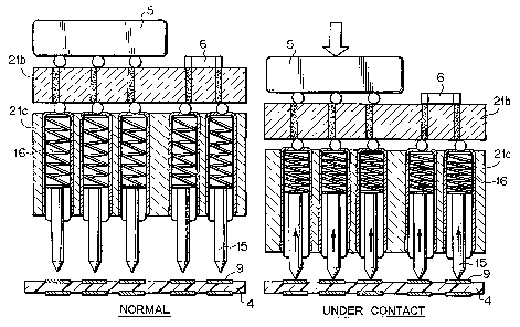
As shown in Fig. 5, each of the probe pins 8 has coil spring 16 and
probe terminal 15 which is pressed by the coil spring 16, and the fixture
portions 21 and 22 arranged at the upper and lower sides of the print board 4
are moved downwardly or upwardly, whereby these probe terminals 15 abut
against the pads 9 of the print board 4. When the probe terminals 15 abut
against the pads 9 of the print board 4 and are further pressed, the probe
terminals 15 are retracted into the probe pins and are pressed against the
pads 9 under fixed pressure by the coil spring 16. As described above, the
equivalent parts such as the RAM 5, the capacitors 6, the resistors 7 and the
print board 4 are electrically connected to one another, and the bare-chip LSI
and the mount parts such as the RAM 5, the capacitors 6 and the resistors 7
are arranged as if they are actually boarded on the print board 4.
Further, under the state that the equivalent parts such as the RAM 5,
the capacitor 6, the resistor 7 and the print board 4 are electrically
connected
to one another, the test signal is transmitted from the controller 1 to the
print
board 4 to perform the high-speed test, thereby examining the bare-chip LSI 3
as to whether the bare-chip LSI 3 can operate normally.
After the examination, the fixture portions 21 and 22 are moved in the
up-and-down direction of the print board 4, and the print board 4 is detached
from the print board- fixing table 14. If the bare-chip LSI 3 operates
normally,
the SMT parts such as RAM, capacitors and resistors are actually mounted on
the print board 4. If the bare-chip LSI 3 does not operate normally, the print
board 4 having the bare-chip LSI 3 concerned is wasted, or it is exchanged by
another one, and the test is carried out again.
Power source portion 11 serves as a power source for the controller 1,
CA 02324135 2000-10-24
_7_
and also serves as a driving power for the fixture driving portion 10.
In the above embodiment, two tester boards are confronted on both
surfaces of the print board. In the case of one surface mounting board, one
tester board may be confronted on the one surface of the print board.
As described above, according to the present invention, at the stage
that the bare-chip LSI is mounted on the print board, the tester boards on
which the equivalent parts corresponding to the SMT parts such as R,AM,
capacitors and resistors to be mounted on the print board are confronted to
the print board from the upper and lower sides of the print board, and the
probes of the respective equivalent parts of the tester boards corresponding
to
the SMT parts are brought into contact with the pads located at the SMT part
mount places on the print board to construct the SMT part quasi-mount state
for the print board. Under this state, the test signal is transmitted from the
controller of the high-speed tester to the bare-chip LSI to perform the high
speed test.
Accordingly, the following effects can be achieved:
A first effect resides in that the functional test at the actual speed of
the bare-chip LSI alone can be performed under the state that only the bare-
chip LSI is secured to the print board. This is because the SMT parts to be
originally mounted on the print board under test are mounted at the fixture
portion side of the high-speed tester and the probes which can operate at a
high frequency and very short time are brought into contact with the print
board to perform the same high-speed operation as the actual operation of the
apparatus.
A second effect resides in that the functional defects can be found at
CA 02324135 2000-10-24
_8_
an early stage and thus the loss of repair can be reduced. This is because the
functional defects which have been hitherto found by the examination of the
apparatus at the final stage can be found at an early stage of the board
manufacturing process with the same high-speed operation test as the actual
apparatus, so that the failure cost of defective boards can be reduced.