Note: Descriptions are shown in the official language in which they were submitted.
1
CA 02324570 2000-10-26 -,
a
BERG2506 PATENT
C2285
WAVEGUIDES AND BACKPLANE SYSTEMS
Field of the Invention
This invention relates to waveguides and backplane systems. More particularly,
the invention relates to broadband microwave modem waveguide backplane
systems.
Background of the Invention
The need for increased system bandwidth for broadband data transmission rates
in telecommunications and data communications backplane systems has led to
several general
technical solutions. A first solution has been to increase the density of
moderate speed parallel
bus structures. Another solution has focused on relatively less dense, high
data rate differential
pair channels. These solutions have yielded still another solution - the all
cable backplanes
that are currently used in some data communications applications. Each of
these solutions,
however, suffers from bandwidth limitations imposed by conductor and printed
circuit board
(PCB) or cable dielectric losses.
The Shannon-Hartley Theorem provides that, for any given broadband data
transmission system protocol, there is usually a linear relationship between
the desired system
data rate (in Gigabits/sec) and the required system 3dB bandwidth (in
Gigahertz). For
example, using fiber channel protocol, the available data rate is
approximately four times the
3 dB system bandwidth. It should be understood that bandwidth considerations
related to
attenuation are usually referenced to the so-called "3dB bandwidth."
Traditional broadband data transmission with bandwidth requirements on the
CA 02324570 2000-10-26
~..J
' BERG2506 - 2 - PATENT
C2285
order of Gigahertz generally use a data modulated microwave carrier in a
"pipe" waveguide
as the physical data channel because such waveguides have lower attenuation
than comparable
cables or PCB's. This type' of data channel can be thought of as a "broadband
microwave
modem" data transmission system in comparison to the broadband digital data
transmission
commonly used on PCB backplane systems. The present invention extends
conventional, air-
filled, rectangular waveguides to a backplane system. These waveguides are
described in
detail below.
Another type of microwave waveguide structure that can be used as a
backplane data channel is the non-radiative dielectric (NRD) waveguide
operating in the
transverse electric 1,0 (TE 1,0) mode. The TE 1,0 NRD waveguide structure can
be
incorporated into a PCB type backplane bus system. This embodiment is also
described in
detail in below. Such broadband microwave modem waveguide backplane systems
have
superior bandwidth and bandwidth-density characteristics relative to the
lowest loss
conventional PCB or cable backplane systems.
1 S An additional advantage of the microwave modem data transmission system
is that the data rate per modulated symbol rate can be multiplied many fold by
data
compression techniques and enhanced :modulation techniques such as K-bit
quadrature
amplitude modulation (QAM), where K=16, 32, 64, etc. It should be understood
that, with
modems (such as telephone modems, for example), the data rate can be increased
almost a
hundred-fold over the physical bandwidth limits of so-called "twisted pair"
telephone lines.
Waveguides have the best transmission characteristics among many
transmission lines, because they have no electromagnetic radiation and
relatively low
attenuation. Waveguides, however, are impractical for circuit boards and
packages for two
major reasons. First, the size is typically too large for a transmission line
to be embedded in
circuit boards. Second, waveguides must be surrounded by metal wails. Vertical
metal wails
cannot be manufactured easily by lamination techniques, a standard fabrication
technique for
circuit boards or packages. Thus, there is a need in the art for a broadband
microwave modem
waveguide backplane systems for laminated printed circuit boards.
CA 02324570 2000-10-26
a '..,J
' BERG2506 - 3 - PATENT
C2285
Summary of the Invention
A waveguide according to the present invention comprises a first conductive
channel disposed along a waveguide axis, and a second conductive channel
disposed generally
parallel to the first channel. A gap is defined between the first and second
channels along the
S waveguide axis. The gap has a gap width that allows propagation along the
waveguide axis
of electromagnetic waves in a TE n,0 mode, wherein n is an odd number, but
suppresses
electromagnetic waves in a TE m,0 mode, wherein m is an even number.
Each channel can have an upper broadwall, a lower broadwall opposite and
generally parallel to the upper broadwall, and a sidewall generally
perpendicular to and
connected to the broadwalls. The upper broadwall of the first channel and the
upper broadwall
of the second channel are generally coplanar, and the gap is defined between
the upper
broadwall of the first channel and the upper broadwall of the second channel.
Similarly, the
lower broadwall of the first channel and the lower broadwall of the second
channel are
generally coplanar, and a second gap is defined between the lower broadwall of
the first
channel and the lower broadwall of the second channel. Thus, the first channel
can have a
generally C-shaped, or generally I-shaped cross-section along the waveguide
axis; and can be
formed by bending a sheet electrically conductive material.
~.
In another aspect of the invention, an NRD waveguide having a gap in its
conductor for mode suppression, comprises an upper conductive plate and a
lower conductive
plate, with a dielectric channel disposed along a waveguide axis between the
conductive
plates. A second channel is disposed along the waveguide axis adjacent to the
dielectric
channel between the conductive plates. The upper conductive plate has a gap
along the
waveguide axis above the dielectric channel. The gap has a gap width that
allows propagation
along the waveguide axis of electromagnetic waves in an odd longitudinal
magnetic mode,
but suppresses electromagnetic waves in an even longitudinal magnetic mode.
A backplane system according to the invention comprises a substrate, such as
a printed circuit board or multilayer board, with a waveguide connected
thereto. The
waveguide can be a non-radiative dielectric waveguide, or an air-filled
rectangularwaveguide.
According to one aspect of the invention, the waveguide has a gap therein for
preventing
propagation of a lower order mode into a higher order mode.
CA 02324570 2000-10-26
i
BERG2506 - 4 - PATENT
C2285
The backplane system includes at least one transmitter connected to the
waveguide for sending an electrical signal along the waveguide, and at least
one receiver
connected to the waveguide for accepting the electrical signal. The
transmitter and the receiver
can be transceivers, such as broadband microwave modems.
Brief Description of the Drawings
The foregoing summary, as well as the following detailed description of the
preferred embodiments, is better understood when read in conjunction with the
appended
drawings. For the purpose of illustrating the invention, there is shown in
the' drawings an
embodiment that is presently preferred, it being understood, however, that the
invention is not
limited to the specific methods and instrumentalities disclosed.
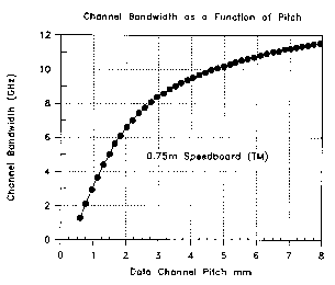
Figure 1 shows a plot of channel bandwidth vs. data channel pitch for a 0.75m
"SPEEDBOARD" backplane.
Figure 2 shows a plot of bandwidth density vs. data channel pitch for a 0.75m
"SPEEDBOARD" backplane.
Figure 3 shows plots ofbandwidth vs. bandwidth density/layer for a 0.5 m FR-
4 backplane, and 1 m and 0.75m "SPEEIjBOARD" backplanes.
Figure 4 shows a schematic of a backplane system in accordance with the
present invention.
Figure 5 depicts a closed, extruded, conducting pipe, rectangular waveguide.
Figure 6 depicts the current flows for the TE 1,0 mode in a closed, extruded,
conducting pipe, rectangular waveguide.
Figure 7A depicts a split rectangular waveguide according to the present
invention.
Figure 7B depicts an air-filled waveguide backplane system according to the
present invention.
Figure 8 shows a plot of attenuation vs. frequency in a rectangular waveguide.
Figure 9 shows plots of the bandwidth and bandwidth density characteristics
of various waveguide backplane systems.
Figure 10 provides the attenuation versus frequency characteristics of
CA 02324570 2000-10-26
Vii; '..J
BERG2506 - 5 - PATENT
C2285
conventional laminated waveguides using various materials.
Figure 11 provides the attentuation versus frequency characteristics of a
backplane system accordirig to the present invention.
Figure 12 provides the attenuation versus frequency characteristics of another
backplane system according to the present invention.
Figure 13A depicts a non-radiative dielectric (NRD.) waveguide.
Figure 13B shows a plot of the field patterns for the odd mode in the
waveguide of Figure 13A.
Figure 14 shows a dispersion plot for the TE 1,0 mode in an NRD waveguide.
Figure 1 SA depicts an NRD waveguide backplane system.
Figure 15B depicts an NRD waveguide backplane system according to the
present invention.
Figure 16 shows a plot of inter-waveguide crosstalk vs. frequency for the
waveguide system of Figure 13A.
Detailed Description of Preferred Embodiments
Example of a Conventional Svstem~ Broadside Coupled Differential Pair PCB Bac
lane
The attenuation {A) of a broadside coupled PCB conductor pair data channel
has two components: a square root of frequency (f) term due to conductor
losses, and a linear
term in frequency arising from dielectric losses. Thus,
A = (A,*SQRT(fj + AZ*f )*L*(8.686 db/neper) (1)
where
~ _ (~*wo*P)°.s ~ (w/p)*p*Zo (2)
and
AZ = ~*DF*(po*E °)°.s, (3)
The data channel pitch is p, w is the trace width, p is the resistivity of the
PCB traces, and s
and DF are the permittivity and dissipation factor of the PCB dielectric,
respectively. For
CA 02324570 2000-10-26
'
BERG2506 - 6 - PATENT
C2285
scaling, w/p is held constant at -0.5 or less and Zo is held constant by
making the layer spacing
between traces, h, proportional to p where h/p = 0.2. The solution of Equation
( 1 ) for A = 3dB
yields the 3dB bandwidth'of the data channel for a specific backplane length,
L.
"SPEEDBOARD," which is manufactured and distributed by Gore, is an
example of a low loss, "TEFLON' laminate. Figure 1 shows a plot of the
bandwidth per
channel for a 0.75m "SPEEDBOARD" backplane as a function of data channel
pitch. As the
data channel pitch, p, decreases, the channel bandwidth also decreases due to
increasing
conductor losses relative to the dielectric losses. For a highly parallel (i.
e., small data channel
pitch) backplane, it is desirable that the density of the parallel channels
increase faster than
the corresponding drop in channel bandwidth. Consequently, the bandwidth
density per
channel layer, B W/p, is of primary concern. It is also desirable that the
total system bandwidth
increase as the density of the parallel channels increases. Figure 2 shows a
plot of bandwidth
density vs. data channel pitch for a 0.75m "SPEEDBOARD" backplane. It can be
seen from
Figure 2, however, that the bandwidth-density reaches a maximum at a channel
pitch of
approximately 1.2 mm. Any change in channel pitch beyond this maximum.results
'in a
decrease in bandwidth density and, consequently, a decrease in system
performance. The
maximum in bandwidth density occurs when the conductor and dielectric losses
are
approximately equal.
The backplane connector performance can be characterized in terms of the
bandwidth vs. bandwidth-density plane, or "phase plane" representation. Plots
of bandwidth
vs. bandwidth density/layer for a O.Sm FR-4 backplane, and for l.Om and 0.75m
"SPEEDBOARD" backplanes are shown in Figure 3, where channel pitch is the
independent
variable. FR-4 is another well-known PCB material, which is a glass reinforced
epoxy resin.
It is evident that, for a given bandwidth density, there are two possible
solutions for channel
bandwidth, i.e., a dense low bandwidth "parallel" solution, and a high
bandwidth "serial"
solution. The limits on bandwidth-density for even high performance PCBs
should be clear
to those of skill in the art.
Backplane Svstem
Figure 4 shows a schematic of a backplane system B in accordance with the
CA 02324570 2000-10-26
~.J
BERG2506 - 7 - PATENT
C2285
present invention. Backplane system B includes a substrate S, such as a
multilayer board
(MLB) or a printed circuit board (PCB). A waveguide W mounts to substrate S,
either on an
outer surface thereof, or as a layer in an inner portion of an MLB (not
shown).
Waveguide W transports electrical signals between one or more transmitters
T and one or more receivers R. Transmitters T and receivers R could be
transceivers and,
preferably, broad band microwave modems.
Preferably, backplane system B uses waveguides having certain characteristics.
The preferred waveguides will now be described.
Air Filled Rectangular WaveQUide Backplane System
Figure 5 depicts a closed, extruded, conducting pipe, rectangular waveguide
10. Waveguide 10 is generally rectangular in cross-section and is disposed
along a waveguide
axis 12 (shown as the z-axis in Figure 5). Waveguide 10 has an upper broadwall
14 disposed
along waveguide axis 12, and a lower broadwall 16 opposite and generally
parallel to upper
broadwall 14. Waveguide 10 has a pair of sidewalls 18A, 188, each of which.is
generally
perpendicular to and connected to broadwalls 12 and 14. Waveguide 10 has a
width a and a
height b. Height b is typically less than width a. The fabrication of such a
waveguide for
backplane applications can be both difficult and expensive.
Figure 6 depicts the'current flows for the TE 1,0 mode in walls 14 and 188 of
waveguide 10. It can be seen from Figure 6 that the maximum current is in the
vicinity of the
edges 20A, 208 of waveguide 10, and that the current in the middle of upper
broadwall 14 is
only longitudinal (i.e., along waveguide axis 12).
According to the present invention, a longitudinal gap is introduced in the
broadwalls so that the current and field patterns for the TE 1,0 mode are
unaffected thereby.
As shown in Figure 7A, a waveguide 100 of the present invention includes a
pair of
conductive channels 102A,102B. First channel 102A is disposed along a
waveguide axis 110.
Second channe1102B is disposed generally parallel to first channel 102A to
define a gap 112
between first channel 102A and second channel 1028.
Gap 112 allows propagation along waveguide axis 110 of electromagnetic
waves in a TE n,0 mode, where n is an odd integer, but suppresses the
propagation of
CA 02324570 2000-10-26
BERG2506 - 8 - PATENT
C2285
electromagnetic waves in a TE n,0 mode, where n is an even integer. Waveguide
100
suppresses the TE n,0 modes for even values of n because gap 112 is at the
position of
maximum transverse current for those modes. Consequently, those modes cannot
propagate
in wave guide 100. Consequently, waves can continue to be propagated in the TE
1,0 mode,
for example, until enough energy builds up to allow the propagation of waves
in the TE 3,0
mode. Because the TE n,0 modes are suppressed for even values of n, waveguide
100 is a
broadband waveguide.
Waveguide 100 has a width a and height b. To ensure suppression of the TE
n,0 modes for even values of n, the height b of waveguide 100 is defined to be
about O.Sa or
less. The data channel pitch p is approximately equal to a. The dimensions of
waveguide 100
can be set for individual applications based on the frequency or frequencies
of interest. Gap
112 can have any width, as long as an interruption of current occurs.
Preferably, gap 112
extends along the entire length of waveguide 100.
As shown in Figure 7A, each channel 102A, 102B has an upper broadwall
104A, 104B, a lower broadwall 106A, 106B opposite and generally parallel to
its upper
broadwall 104A,104B, and a sidewall 108A,108B generally perpendicular to and
connected
to broadwalls 104, 106. Upper broadv~rall 104A of first channell02A and upper
broadwall
104B of second channel 102B are generally coplanar. Gap 112 is defined between
upper
broadwall 104A of first channel 102A and upper broadwall 104B of the second
channel 102B.
Similarly, lower broadwall 106A of first channel 102A and lower broadwall 106B
of second
channel 102B are generally coplanar, with a second gap 114 defined
therebetween. Sidewall
108A of first channel 102A is opposite and generally parallel to sidewall 108B
of second
channel 102B. Side wails 108A and 108B are disposed opposite one another to
form
boundaries of waveguide 100.
An array of waveguides 100 can then be used to form a backplane system120
as shown in Figure 7B. Backplane system 120 can be constructed using a
plurality of
generally "I" shaped conductive channels 103 or "C" shaped conductive channels
102.
Preferably, the conductive channels are made from a conductive material, such
as copper,
which can be fabricated by extrusion or by bending a sheet of conductive
material. The
conductive channels can then be laminated (by gluing, for example), between
two substrates
CA 02324570 2000-10-26
/ v...~
BERG2506 - 9 - PATENT
C2285
118A,118B, which, in a preferred embodiment, are printed circuit boards
(PCBs). The PCBs
could have, for example, conventional circuit traces (not shown) thereon.
Unlike the conventional. systems described above; the attenuation in a
waveguide 110 of present invention is less than 0.2 dB/meter and is not the
limiting factor on
bandwidth for backplane systems on the order of one meter long. Instead, the
bandwidth
limiting factor is mode conversion from a low order mode to the next higher
mode caused by
discontinuities or, irregularities along the waveguide. (Implicit in the
following analysis of
waveguide systems is the assumption of single, upper-sideband modulation with
or without
carrier suppression.)
Figure 8 is a plot of attenuation vs. frequency in a rectangular waveguide 100
according to the present invention. It can be seen from Figure 8 that the
lowest operating
frequency, f~, that avoids severe attenuation near cutoff is approximately
twice the TE 1,0
cutoff frequency, fc, or
fc < f~ s 2*(c/2a) = c/a (4).
The cutofffrequency for the TE 3,0 made, which is the next higher mode because
of gap 112,
is three times the TE 1,0 cutoff frequency or
~" = 3*(c/2a) =1.5*fo (5).
The bandwidth, BW, based on the upper sideband limit, is then (~"-f~), which,
on substitution
for c, the speed of light, is
BW = 150 (Ghz*mm)/p, (6)
where p, the data channel pitch, has been substituted for a, the waveguide
width. Again, b/p
is defined to be less than 0.5 to suppress TE O,n modes. The bandwidth
density, BWD, is
simply the bandwith divided by the pitch or
CA 02324570 2000-10-26
,......%
BERG-2506 -10 - PATENT
C2285
BWD = BW/p = 150 / p*p (Ghz/mm) (7).
Then the relationship between BW and BWD is
BW = (150*BWD)°.s (Ghz) (8),
A plot of this relationship, corresponding to a frequency range of, for
example,
about 20 GHz to about 50 GHz, is shown relative to the bandwidth vs bandwidth
density
performance of a "SPEEDBOARD" backplane in Figure 9. It can be seen from
Figure 9 that
the bandwidth and bandwidth-density range obtainable with the rectangular TE
1,0 mode
backplane system is approximately twice that of the "SPEEDBOARD" system.
Figures 10-12 also demonstrate the improvement that the present invention can
have over conventional systems. Figure 10 provides the attenuation versus
frequency
characteristics of conventional laminated waveguides using various materials.
Figure 11
provides the attentuation versus frequency characteristics of a backplane
system according to
the present invention, specifically a 0.312" by 0.857" slotted waveguide using
a 0.094"
diameter copper tubing probe with Sh l 8 penetration at ~I 0.4 GHz. Figure 12
provides the
attenuation versus frequency characteristics of another backplane system
according to the
present invention, this time using a doorknob-type antenna.
These figures demonstrate that the waveguides of the present invention have
greater relative bandwidth than conventional systems.
Although described in this section as an "air filled" waveguide, the present
invention could use filler material in lieu of air. The filler material could
be any suitable
dielectric material.
NonRadiative Dielectric (NRDI Wavesuide Bac lane System
Figure 13A shows a conventional TE mode NRD waveguide 20. Waveguide
20 is derived from a rectangular waveguide (such as waveguide 10 described
above), partially
filled with a dielectric material 22, with the sidewalls removed. As shown,
waveguide 20
includes an upper conductive plate 24U, and a lower conductive plate 24L
disposed opposite
CA 02324570 2000-10-26
BERG2506 -11- PATENT
C2285
and generally parallel to upper plate 24U. Dielectric channel 22 is disposed
along a waveguide
axis 30 (shown as the z-axis in Figure 13A) between conductive plates 24U and
24L. A
second channel 26 is disposed along waveguide axis 30 adjacent to dielectric
channel 22. U.S.
Patent Number 5,473,296, incorporated herein by reference, describes the
manufacture of
NRD waveguides.
Waveguide 20 can support both an even and an odd longitudinal magnetic
mode (relative to the symmetry of the magnetic field in the direction of
propagation). The
even mode has a cutoff frequency, while the odd mode does not. The field
patterns in
waveguide 20 for the desired odd mode are shown in Figure 13B. The fields in
dielectric 22
are similar to those of the TE 1,0 mode in rectangular waveguide 10 described
above, and vary
as Ey ~ cos(lot) and HZ ~ sin(lac). Outside of dielectric 22, however, the
fields decay
exponentially with x, i. e., exp(-Tx), because of the reactive loading of the
air spaces on the left
and right faces 22L, 22R of dielectric 22.
The dispersion characteristic of this mode for a "TEFLON" guide is shown in
Figure 14, where Beta and F are the normalized propagation constant and
normalized
frequency, respectively. That is,
Beta = a~i/2 (9)
and
F = (a~/2c)(Dr-1)~.s, ( 10)
where c is the speed of light, and Dr is the relative dielectric constant of
dielectric 22. The
range of operation is for values of f between 1 and 2 where there is only
moderate dispersion.
Since the fields outside of dielectric 22 decay exponentially, two or more NRD
waveguides 30 can be laminated between substrates 24U, 24L, such as ground
plane PCBs,
to form a periodic multiple bus structure as illustrated in Figure 15A. The
first order
consequence of the coupling of the fields external to dielectric 22 is some
level of crosstalk
between the dielectric waveguides 30. This coupling decreases with increasing
pitch, p, and
frequency, F, as illustrated in Figure 16. Therefore, the acceptable crosstalk
levels determine
the minimum waveguide pitch pm;".
CA 02324570 2000-10-26
a
BERG2506 -12 - PATENT
C2285
According to the present invention, and as shown in Figure 1 SB, a
longitudinal
gap can be used to prevent the excitation and subsequent propagation of the
higher order even
mode, which has a transverse current maximum in the top and bottom ground
plane structures
at x = 0. Figure 15B depicts an NRD waveguide backplane system 120 of the
present
invention. Waveguide backplane system 120 includes an upper conductive plate
124U, and
a lower conductive plate 124L disposed opposite and generally parallel to
upper plate 124U.
Preferably, plates 124U and 124L are made from a suitable conducting material,
such as a
copper alloy, and are grounded.
A dielectric channel 122 is disposed along a waveguide axis 130 between
conductive plates 124U and 124L. Gaps 128 in the conductive plates are formed
along
waveguide axis 130. Preferably, gaps 128 are disposed near the middle of each
dielectric
channel 122. An air-filled channel 126 is disposed along waveguide axis 130
adjacent to
dielectric channel 122. In a preferred embodiment, waveguide 120 can include a
plurality of
dielectric channels 122 separated by air-filled channels 126. Dielectric
channels 122 could be
made from any suitable material.
The bandwidth of the TE 1,0 mode NRD waveguide is dependent on the losses
in dielectric and the conducting ground planes. For the case where b ~ a/2,
and the
approximation to the eigenvalue
k ~ (ce~/c)(Dr- 1 )° .s ~ 2/a, ( 11 )
holds, the attenuation has two components: a linear term in frequency
proportional to the
dielectric loss tangent, and a 3/2 power term in frequency due to losses in
the conducting
ground planes. For an attenuation of this form
a = (ai)(~l.s + (ax)f (12)
the bandwidth-length product, BW*L, based on the upper side-band 3 dB point is
BW*L ~ (0.345/ai) I (1/2)(a, lai)(f°)°.s + 1 (13)
CA 02324570 2000-10-26
u' ~J
BERG2506 -13 - PATENT
C2285
where BW/f~ < 1, and f~ is the nominal Garner frequency. Preferably, pitch p
is a multiple of
width a. Then, from (3), fo is proportional to l/p. Also, bandwidth density
BWD = BW/p.
Plots of the bandwidth end bandwidth density characteristics for a "TEFLON'
NRD
waveguide, and for a Quartz NRD guide having Dr = 4 and a loss tangent of
0.0001. are shown
in Figure 9. For these plots p = 3a. Thus, like the characteristics of
rectangular waveguide
100, NRD waveguide 120 offers increased bandwidth and, more importantly, an
open ended
bandwidth density characteristic relative to the parabolically closed
bandwidth performance
of conventional PCB backplanes.
Thus, there have been disclosed broadband microwave modem waveguide
backplane systems for laminated printed circuit boards. Those skilled in the
art will appreciate
that numerous changes and modifications may be made to the preferred
embodiments of the
invention and that such changes and modifications may be made without
departing from the
spirit of the invention. For example, Figure 9 also includes a reference point
for a minimum
performance, mufti-mode fiber optic system which marks the lower boundary of
fiber optic
systems potential bandwidth performance. It is anticipated that the microwave
modem
waveguides of the present invention can provide a bridge in bandwidth
performance between
conventional PCB backplanes and future fiber optic backplane systems. It is
therefore
intended that the appended claims cover all such equivalent variations as fall
within the true
spirit and scope of the invention.