Note: Descriptions are shown in the official language in which they were submitted.
CA 02324675 2000-10-26
A SDBSTRATS FOR I~OUHTING AN OPTICAL COMPONgNT, A 1~T80D FOR
PRODUCING Tip SAID, AND AN OPTICAL I~ODULS USING THg SAID
BACKGROUND OF THS INVENTION
This invention relates to a substrate which is mountable
with an optical component such as optical semiconductor device
and optical device including optical fiber and lens, a method
for producing such a substrate, and an optical module using such
a substrate.
In recent years, there has been the demand for larger
capacity and more functions of optical communication systems
and, accordingly, miniaturization, higher integration and lower
production costs have been required for optical devices such as
optical transmitters and optical receivers. Particularly, in
order to reduce the assembling cost of optical devices,
attention has been given to the technique for mounting optical
components such as optical semiconductor devices, optical fibers
and lenses on a single substrate, in particular, to the so-
called passive alignment technique such as an optical hybrid
mounting technique, and an alignment-free mounting technique
using a silicone platform.
According to the above techniques, an optical axis
adjustment and an optical coupling can be established without an
aligning operation only by mounting optical components on the
substrate with respect to a positioning groove formed in the
1
CA 02324675 2000-10-26
substrate or mounting optical components in mounting grooves
formed in the substrate. This enables a significant reduction
in the assembling costs. In order to mount optical components
without aligning operation, the optical component mounting
grooves formed in the substrate are required to have highly
precise dimensions of top opening width and depth. Further, the
relative positional relationship between the grooves is required
to be precise in the order of sub-micrometers or less than one
millionth of a meter.
However, there has been the big problem that a plurality of
grooves whose respective depths are different from each other
cannot be simultaneously made by a single etching operation for
the following reasons.
Generally, in the case where a groove is made in a
substrate made of a silicon monocrystal by an etching, there
will occur an undercut 100 below the non-patterned photoresist
layer 200 as shown in FIG. 8. More specifically, in the case
that a V-shaped groove is formed in a substrate made of a
silicon monocrystal having a (100) surface as a principle
surface by anisotropic etching using an alkaline solution
(etching solution: KOH (43 vol%) solution, solution temperature
60°C ) , an undercut occurs in proportion to the depth of etching
as can be seen from a graph of FIG. 9.
The undercut amount represented by the vertical axis in
FIG. 9 means a difference between a designed pattern width and
2
CA 02324675 2000-10-26
r~.
an actual top opening width (V-shaped groove width) of a V-
shaped groove after etching. It will be seen from FIG. 8 that
the undercut amount (2L) is calculated by subtracting a designed
width (DW) of the patterned hole from an actual width (AW) of
the V-shaped groove, that is, 2L = AW - DW. To make a groove
having a depth of 800 ucn, for example, it is necessary to apply
etching for approximately 50 hours , and an undercut of about 30
um occurs during this etching. It means that in the case of
making a groove having a final depth of 30 dun, the designed
pattern width should be at 0 um. This is to say that a groove
having a width of 30um or smaller cannot be practically made.
The occurrence of undercuts will make it impossible to form a
plurality of grooves having different depths in a single
substrate by a single etching.
Further, in the case of making a plurality of grooves
having trapezoidal cross sections and different depths to their
bottom surfaces, it has been difficult to simultaneously form
them by a single etching.
In view of this problem, a substrate for mounting an
optical component (hereinafter, referred to as "optical
component mounting substrate") which is formed with different
depth grooves has been conventionally produced by steps shown in
FIGS. 10A to 10E. In order to facilitate the description, in
these figures, forming of two V-shaped grooves in a substrate
will be described.
3
CA 02324675 2000-10-26
First, as shown in FIG. 10A, a protection film 52 made of a
silicon oxide or a silicon nitride is formed on the entire top
surface of a substrate 51 made of a silicon monocrystal. The
protection film 52 is resistant to an etching solution for
etching the substrate 51. Further, a photoresist film 53 is
formed on the entire top surface of the protection film 52.
Patterning is applied to the photoresist film 53 by
_ photolithography using a photomask for part of a V-shaped groove
to be formed in a first etching. Thereafter, the part of the
protection film 52 which corresponds to the V-shaped groove is
also removed by a silicon oxide etching solution.
Subsequently, as shown in FIG. 10B, a V-shaped groove 54 is
formed by etching the surface part where the substrate 51 is
exposed using an etching solution containing sodium hydroxide
(NaOH), potassium hydroxide (KOH), tetramethylammonium hydroxide
(TMAH), etc.
Subsequently, as shown in FIG. 10C, a protection film 55
made of a silicon oxide or a silicon nitride is formed on the
entire top surface of the substrate 51 including the V-shaped
groove 54 after the protection film 52 is entirely removed, and
a photoresist film 56 is formed on the entire top surface of the
protection film 55. A photomask for a V-shaped groove to be
formed in a second etching is positioned with reference to a
marker provided on the substrate 51 to position the photomask,
and patterning is applied to the photoresist film 56 by
4
CA 02324675 2000-10-26
photolithography. Thereafter, the part of the protection film
55 which corresponds to the groove to be formed by the second
etching is removed.
Subsequently, as shown in FIG. 10D, a groove 57 is formed
by the same procedure as the V-shaped groove 54, and the
protection film 55 is finally removed to produce an optical
component mounting substrate Jl formed with the grooves as shown
in FIG. 10E.
In the above-mentioned conventional method, it will be
apparent that high-precision patterning cannot be accomplished
for the second formed photoresist film 56 and protection film 55
because of the presence of the V-shaped groove 54 formed in the
first etching. In view of this problem, Japanese Unexamined
Patent Publication No. 3-132031 proposes making of a plurality
of V-shaped grooves having different depths by applying
patterning only to the top flat surface of the substrate.
However, this proposal cannot successfully eliminate the
likelihood that the position of a second-placed photomask is
different from that of a first-placed photomask, which causes
undesired displacement of V-shaped grooves having different
depths.
Specifically, a reference marker is provided at a specified
position of the substrate, e.g., at an end of the substrate. In
the first and second etchings, the photomask is arranged over
the substrate by positioning a marker provided on the photomask
CA 02324675 2000-10-26
with respect to the reference marker on the substrate. The
photoresist film or protection film is likely to have an
irregular thickness around the previously-formed groove, which
makes it difficult to distinguish the marker provided on the
substrate. Further, an exposure device, e.g., a contact-type
exposure device, is usually incapable of positioning in the
order of sub-microns.
Even if the above problems could be cleared, the substrate
is liable to be warped due to a heat history since the
positioning marker provided on the substrate have been subjected
to various heat treatment processes. This warping causes shift
of the positioning marker.
It will be seen to be extremely difficult to make the
marker provided on the photomask agree with the marker provided
on the substrate. Accordingly, in the above-mentioned
conventional method, the greater the number of grooves having
different depths becomes, the greater the number of placing
photomask becomes, which consequently accumulates displacements
of markers, and finally results in the unacceptable disagreement
among grooves.
SnI~IARY OF TIC I1~1VBNTION
It is an object of the present invention to provide a
substrate for mounting an optical component, a method for
producing an optical component mounting substrate, and an
6
CA 02324675 2000-10-26
optical module which are free from the problems residing in the
prior art.
According to the invention, a substrate for mounting an
optical component is formed with a first groove and a second
groove at least. The second groove has a depth greater than the
first groove. The first groove and the second groove have a
relationship with each other represented by the following
- equation,
(2Dsin9)/R s C
where D denotes a depth of the first groove, 8 denotes an angle
between a horizontal plane and a slanted surface of the first
groove (0°<8<90°), R - F/E (E denotes an etching rate of a
slanted surface of the first groove, F denotes an etching rate
of a bottom surface of the groove, C denotes a top opening width
of the groove.
The first groove and the second grooves are formed by
forming a protection film on an entire top surface of the
substrate, forming pattern holes corresponding to the first and
second grooves in the protection film by a single mask having
holes corresponding to the first and second grooves, forming a
protection seal on a pattern hole corresponding to one of the
first and second grooves, applying anisotropic etching to the
substrate through the not-sealed pattern hole to thereby form
the other of the first and second grooves, removing the
protection seal, forming another protection seal on the groove
7
CA 02324675 2006-06-15
formed by anisotropic etching, applying anisotropic etching to
the substrate through the seal-removed pattern hole to thereby
form the remaining one of the first and second grooves, and
removing the protection film and the another protection seal
from the substrate.
The inventive substrate is mounted with an optical component
to produce an inventive optical module.
Thus, an optical component mounting substrate formed with a
plurality of grooves having different sizes and depths can be
formed to have highly precisely dimensions. Further, optical
devices can be accurately mounted on the substrate, thereby
enabling production of an optical module having an excellent
performance.
Accordingly, in one aspect the present invention resides in
a substrate for mounting an optical component, comprising:
a first groove formed in a top surface of the substrate;
a second groove formed in the top surface of the substrate,
the second groove having a depth greater than the first groove;
the first groove and the second groove having a
relationship with each other represented by the following
equation,
(2DsinA) /R >_ C
where D denotes a depth of the second groove, 8 denotes an angle
between a horizontal plane and a slanted surface of the second
groove (0°<6<90°), R = F/E and E denotes an etching rate of the
8
CA 02324675 2006-06-15
slanted surface of the second groove, F denotes an etching rate
of a bottom surface of the second groove, C denotes a top
opening width of the first groove;
wherein the first and second grooves are formed by:
forming a protection film on substantially the entirety of
the top surface of the substrate;
forming pattern holes corresponding to the first and second
grooves in the protection film by a single mask having holes
corresponding to the first and second grooves;
forming a first protection seal on a pattern hole
corresponding to one of the first and second grooves;
applying anisotropic etching to the substrate through the
not-sealed pattern hole to thereby form the other of the first
and second grooves;
removing the first protection seal;
forming a second protection seal on the groove formed by
anisotropic etching;
applying anisotropic etching to the substrate through the
seal-removed pattern hole to thereby form the remaining one of
the first and second grooves; and
removing the protection film and the second protection seal
from the substrate.
In another aspect, the present invention resides in a method
for producing a substrate having at least a first groove and a
8a
CA 02324675 2006-06-15
second groove whose depth is greater than that of the first
groove, comprising the steps:
forming a protection film on an entire top surface of the
substrate;
forming pattern holes corresponding to the first and second
grooves to be formed in the protection film by a single mask
having holes corresponding to the first and second grooves to be
formed;
forming a first protection seal on a pattern hole
corresponding to one of the first and second grooves;
applying anisotropic etching to the substrate through the
not-sealed pattern hole to thereby form the other of the first
and second grooves;
removing the first protection seal;
forming a second protection seal on the groove formed by
anisotropic etching;
applying anisotropic etching to the substrate through the
seal-removed pattern hole to thereby form the remaining one of
the first and second grooves; and
removing the protection film and the second protection seal
from the substrate.
In a further aspect, the present invention resides in an
optical module comprising:
a substrate including:
8b
CA 02324675 2006-06-15
a first groove formed in a top surface of the
substrate;
a second groove formed in the top surface of the
substrate, the second groove having a depth greater than
the first groove;
the first groove and the second groove having a
relationship with each other represented by the following
equation,
(2Dsin9) /R >_ C
where D denotes a depth of the second groove, A denotes
an angle between a horizontal plane and a slanted surface
of the second groove (0°<6<90°), R = F/E and E denotes an
etching rate of the slanted surface of the second groove, F
denotes an etching rate of a bottom surface of the second
groove, C denotes a top opening width of the first groove;
wherein the first and second grooves are formed by:
forming a protection film on substantially the
entirety of the top surface of the substrate;
forming pattern holes corresponding to the first and
second grooves in the protection film by a single mask
having holes corresponding to the first and second grooves;
forming a first protection seal on a pattern hole
corresponding to one of the first and second grooves;
8c
CA 02324675 2006-06-15
applying anisotropic etching to the substrate through
the not-sealed pattern hole to thereby form the other of
the first and second grooves;
removing the first protection seal;
forming a second protection seal on the groove formed
by anisotropic etching;
applying anisotropic etching to the substrate through
the seal-removed pattern hole to thereby form the remaining
one of the first and second grooves; and
removing the protection film and the second protection
seal from the substrate; and
an optical component mounted on the second groove.
These and other objects, features and advantages of the
present invention will become more apparent upon a reading of
the following detailed description and accompanying drawings.
BRIEF DESCRIPTION OF THE DRAWINGS
FIG. 1 is a plan view showing a part of an optical component
mounting substrate according to an embodiment of the invention;
FIGS. 2A to 2E are sectional views showing an optical
component mounting substrate production method according to the
embodiment of the invention;
8d
CA 02324675 2000-10-26
FIG. 3 is a plan view showing a part of an optical
component mounting substrate according to another embodiment of
the invention;
FIG. 4 is a plan view showing an optical component mounting
substrate according to still another embodiment of the
invention;
FIGS. 5A and 5B are plan views showing photomask patterns
for forming protection seals in the production of the optical
component mounting substrate of FIG. 4, respectively;
FIG. 6A is a plan view showing an optical component
mounting substrate according to further embodiment of the
invention;
FIG. 6B is a sectional view taken along the line 6B-6B in
FIG. 6A;
FIG. 6C is a sectional view taken along the line 6C-6C in
FIG. 6A;
FIG. 6D is a plan view showing a photomask for the
substrate of FIG. 6A;
FIG. 7 is a plan view showing an optical module according
to still further embodiment of the invention, using the optical
component mounting substrate shown in FIG. l;
FIG. 8 is a sectional diagram showing a relationship
between the undercut amount and the pattern width in a V-shaped
groove;
9
CA 02324675 2000-10-26
A
FIG. 9 is a graph showing a relationship between the
undercut amount and the depth of etching in anisotropic etching
of a silicon monocrystal; and
FIGS. 10A to 10E are sectional views showing a conventional
method for producing an optical component mounting substrate.
D$TAILSD DESCRIPTION OF THB PRSFBRRSD S~DIMBNT OF TH8
INVENTION
Inventors of this invention have performed trial and error
to produce an optical component mounting substrate having
grooves whose depths are different from one another at a reduced
cost and accurately. Finally, they have found out tie fact that
to maintain the displacement of a plurality of grooves within 1
lun or smaller, the plurality of grooves having the relationship
defined by Equation ( 1 ) may be formed by a single etching, but
the plurality of grooves having the relationship defined by
Equation (2) must be formed by separate etchings:
(2Dsin9)/R < C (1)
(2Dsin6)/R Z C (2)
wherein D denotes a depth of the deepest one among the plurality
of grooves, A denotes an angle between a horizontal plane and a
slanted surface of the deepest groove (0°<9<90°), R - F/E (E
denotes an etching rate of the slanted surface of the deepest
groove, F denotes an etching rate of the bottom surface of the
deepest groove, and C denotes a top opening width of another one
CA 02324675 2000-10-26
among the plurality of grooves. In the case of a silicon
monocrystal substrate having a (100) surface as a principle
surface, E denotes an etching rate of {111} surface, and F
denotes an etching rate of (100) surface.
Further, the inventor has invented the novel method which
can reduce the number of photomask placements even if a
plurality of etching operations are required. Specifically,
after patterning of a plurality of grooves having a different
depths is executed by a single photomask, etching-resistant seal
is formed on groove forming areas except those where arbitrary
grooves are to be formed in a first etching operation.
Thereafter, the arbitrary grooves are formed by the first
etching operation, and then the following steps (A) and (B) are
performed at least once:
(A) Step of forming etching-resistant seals on the
already formed grooves and/ or groove forming areas except those
where arbitrary grooves are to be formed in next etching
operation; and
(B) Step of forming the remaining one or more V-shaped
grooves by anisotropic etching.
Next, preferred embodiments of the invention mill be
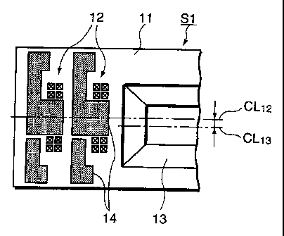
described. Referring to FIG. 1, an optical component mounting
substrate S1 according to an embodiment of the invention
includes a substrate 11 made of a silicon monocrystal to which
anisotropic etching is applicable, small and shallow V-shaped
11
CA 02324675 2000-10-26
grooves 12 formed in the substrate 11 and having a width of,
e.g., 10 um used as positioning markers when optical
semiconductor devices (not shown) such as light emitters and
light detectors are mounted, and a wider and deeper V-shaped
groove 13 formed in the substrate 11 and having a width of,
e.g., 1520 um for mounting a fiber stub, a lens, or the like as
an optical waveguide for optical coupling with the optical
semiconductor devices, and electrode patterns 14 provided on the
substrate 1l for electrically connecting the optical
semiconductor devices with external circuits.
The positioning V-shaped groove 12 and the optical
component mounting V-shaped groove 13 have the following
relationship:
(2Dsin9)/R Z C
wherein D denotes a depth of the V-shaped groove 13 , 8 denotes
an angle between a horizontal plane and a slanted surface of the
V-shaped groove 13 (0°<9<90°), R = F/E (E denotes an
etching rate
of the slanted surface of the V-shaped groove 13, F denotes an
etching rate of the bottom surface of the V-shaped groove 13,
and C denotes a top opening width of the V-shaped groove 12.
The displacement of the center line CL1, of the V-shaped groove
13 with respect to the center line CL12 of the V-shaped groove 12
is equal or smaller than 1 ~.un.
Comparing to a conventional optical component mounting
substrate provided with an electrode marker which is formed at
12
CA 02324675 2000-10-26
the same time as forming an electrode pattern, the inventive
optical component mounting substrate Sl is formed with the V-
shaped grooves 12 serving as reference marker. Accordingly, the
edge of the marker has a satisfactory linearity and can be
highly precisely detected.
With reference to FIGS. 2A to 2E, an exemplary production
method of producing the optical component mounting substrate
- shown in FIG. 1 will be described.
First, as shown in FIG. 2A, a protection film 22 made of a
silicon oxide or a silicon nitride is formed on an entire top
surface of the substrate 11 made of a silicon monocrystal, and a
photoresist film 23 is successively formed on the protection
film 22. Subsequently, the photoresist film 23 is patterned by
photolithography using a photomask formed with openings for the
V-shaped grooves 12 to be formed in a first etching operation
and an opening for the V-shaped groove 13 to be formed in a
second etching operation.
Subsequently, as shown in FIG. 2B, the protection film 22
is patterned by a silicon oxide etching solution, thereby
forming a hole 12a corresponding to the V-shaped groove 12 and a
hole 13a corresponding to the V-shaped groove l3. Thereafter,
an etching-resistant seal 24 made of a silicon oxide or a
silicon nitride is formed over the hole 13a to protect only the
area of the substrate 11 that corresponds to the V-shaped groove
13 to be formed in the second etching.
13
CA 02324675 2000-10-26
Subsequently, as shown in FIG. 2C, anisotropic etching is
applied to an exposed part of the substrate 11 in the hole 12a
using an etching solution containing a sodium hydroxide
solution, a potassium hydroxide solution or the like, thereby
forming a V-shaped groove 25. In this way, the first etching
is performed.
Subsequently, as shown in FIG. 2D, a protection seal 27
made of silicon oxide or silicon nitride is formed on the formed
over the V-shaped groove 12, and the protection seal 26 is
removed. An exposed part of the substrate 11 in the hole 13a is
removed by the same way as the V-shaped groove 12 is formed. In
this way, the second etching is accomplished.
By removing the protection film 22, finally, the optical
component mounting substrate Sl formed with the V-shaped grooves
12 and l3 is produced as shown in FIG. 2E.
According to an actually performed example where V-shaped
grooves having a top opening width of 10 um and a V-shaped
groove having a top opening width of 1520 pm are formed in a
substrate made of silicon monocrystal by the above-described
inventive production method, etching was applied for 39 hours to
form the deeper V-shaped groove 13, an undercut amount during
this etching was 21 um and an actual measurement value of a
relative displacement was 0.6 um.
It should be noted that if the V-shaped groove 12 and the
V-shaped groove 13 has the following relationship:
14
CA 02324675 2000-10-26
(2Dsin8)/R < C
it may be possible to form the V-shaped groove 12 and the V-
shaped groove 13 in the first etching without forming the
protection seal 24.
Also, it may be preferable to form the shallow V-shaped
groove 12 prior to the forming of the deep V-shaped groove 13
because the protection seal for the shallow V-shaped groove 12
can be more precisely formed, with the result that the V-shaped
grooves 12 and 13 can be highly precisely formed.
Next, an optical component mounting substrate according to
another embodiment of the invention will be described. As shown
in FIG. 3, an optical component mounting substrate S2 includes a
small and shallow V-shaped groove 32 having a width of, e.g., 25
pm for ensuring an optical path at an optically coupled portion,
and a larger and deeper V-shaped groove 33 continuous with the
V-shaped groove 32, having a width of, e.g., 1520 ~.un and used to
mount a fiber stub as an optical waveguide. The V-shaped
groove 32 and the V-shaped groove 33 have the same relationship
as the foregoing embodiment, that is:
(2Dsin8)/R z C.
Also, the optical component mounting substrate S2 is
produced in the method similar to the foregoing embodiment, that
is, the method shown in FIG. 2. In this embodiment, the canter
line CL3z of the V-shaped groove 32 and the center line CL;, of
CA 02324675 2000-10-26
the V-shaped groove 33 can be aligned within a desired allowance
of 1 dun or smaller .
Next, an optical component mounting substrate according to
still another embodiment of the invention is described with
reference to FIG. 4. An optical component mounting substrate S3
shown in FIG. 4 is formed with V-shaped grooves 42 serving as
positioning marker, V-shaped grooves 43 for mounting optical
fiber, and V-shaped grooves 44 and 45 for mounting optical
devices constituting a lens system for optical coupling. The
group of V-shaped grooves 42 and 43 and the group of V-shaped
grooves 44 and 45 have the same relationship as the foregoing
embodiments, that is:
(2Dsin6)/R Z C.
Also, the optical component mounting substrate S3 is produced in
the method similar to the foregoing embodiment, that is, the
method shown in FIG. 2. In this embodiment, the respective
center lines CL,~, CL,,3, CL", CL,s of the V-shaped grooves 42 to
45 can be aligned within the allowable range of 1 dun or smaller.
Accordingly, optical devices such as optical fiber, ball lens,
isolator and filter can be aligned accurately without requiring
active adjustment of optical axes.
FIGS. 5A and 5B show photomasks used to form protection
seals, wherein FIG. 5A shows a photomask used to form a
protection seal for the V-shaped grooves 42, 43, and FIG. 5B
16
CA 02324675 2000-10-26
shows a photomask used to form a protection seal for the V-
shaped grooves 44, 45.
First, pattern holes for the V-shaped grooves 42 to 45 are
formed in a photoresist film by a single photomask, and then
formed in a protection film. The V-shaped grooves 42 and 43
are formed in the first etching while protecting the pattern
holes for the V-shaped grooves 44 and 45 by protection seals
which are formed by using the photomask of FIG. 5B. Further, in
the second etching, the V-shaped grooves 44 and 45 are formed
while protecting the pattern holes for the V-shaped grooves 42
and 43 by protection seals which are formed by using the
photomask of FIG. 5A.
FIGS. 6A to 6C show an optical component mounting substrate
according to further embodiment of the invention. An optical
component mounting substrate S4 includes a groove 92 for
mounting a photodiode for monitoring, a groove 93 for mounting a
semiconductor laser, and a V-shaped groove 94 for mounting an
optical fiber. The grooves 92 and 93 have a trapezoid shape
while the groove 94 has a v-shape. Also, the groove 92, the
groove 93, and the groove 94 have the same relationship with one
another as the foregoing embodiments, that is:
(2Dsin9)/R a C.
Also, the optical component mounting substrate S4 is produced in
the method similar to the foregoing embodiment, that is, the
method shown in FIG. 2. In this embodiment, however,
17
CA 02324675 2000-10-26
anisotropic etching is performed three times. Specifically, a
first etching is performed for forming the V-shaped groove 94, a
second etching is performed for forming the groove 93, and a
third etching is performed for forming the groove 92.
FIG. 6D shows a photomask for forming pattern holes
corresponding to the grooves 92 to 94 in a photoresist film in
the initial stage.
The precision in the depth of the grooves 92, 93 and the
precision of their positions with respect to the V-shaped groove
94 are required to be in the order of sub-microns because these
grooves are used for positioning the optical coupling system
with respect to height direction and horizontal direction. The
optical component mounting substrate S4 produced by the
inventive method can satisfy this requirement because the
respective center lines CLg2, CL93, CL9, of the grooves 92 to 94
are aligned within the allowable range of 1 ~.un or smaller.
An optical coupling system free from an active adjustment
of optical axes can be realized only by mounting a semiconductor
laser, a photodiode for monitoring in the grooves 93 and 92
having different depths and widths from the V-shaped groove 94
for mounting an optical fiber.
An optical module according to still further embodiment of
the invention will be described with reference to FIG. 7. The
optical module shown in FIG. 7 is assembled as follows. First,
using the substrate S1 described with reference to FIG. 1, a
18
CA 02324675 2000-10-26
semiconductor laser 101 and a photodiode for monitoring 102 are
soldered and fixed by means of a mounting device such as flip-
chip bonder while observing positioning markers. At this time,
an Au-Sn alloy solder provided on the electrodes 14 are used as
the fixing solder. Further, a collimating lens 103 or the like
is mounted in the deeper groove 13 for mounting an optical
component. As described above, since the positioning markers 12
and the deeper V-shaped groove 13 are so formed as to have a
highly precise relative positional relationship, all optical
axes can be aligned only by mounting the optical components on a
desirably designed substrate. Thus, a highly efficient optical
coupling system can be constructed.
It should be noted that the invention is applicable to
optical component mounting substrates formed with two or more
grooves which have the above-mentioned particular relationship
between them.
As described above, an inventive optical component mounting
substrate is formed with a first groove and a second groove in a
surface thereof at least. The second groove has a depth greater
than the first groove, and the first groove and the second
groove have a relationship with each other represented by the
following equation,
(2Dsin9)/R Z C
where D denotes a depth of the first groove, 8 denotes an angle
between a horizontal plane and a slanted surface of the first
19
/'~.
CA 02324675 2000-10-26
groove (0°<8<90°), R = F/E (E denotes an etching rate of a
slanted surface of the first groove, F denotes an etching rate
of a bottom surface of the groove, C denotes a top opening width
of the groove.
The first and second grooves are formed by forming a
protection film on an entire top surface of the substrate;
forming pattern holes corresponding to the first and second
grooves in the protection film by a single mask having holes
corresponding to the first and second grooves; forming a
protection seal on a pattern hole corresponding to one of the
first and second grooves; applying anisotropic etching to the
substrate through the not-sealed pattern hole to thereby form
the other of the first and second grooves; removing the
protection seal; forming another protection seal on the groove
formed by anisotropic etching; applying anisotropic etching to
the substrate through the seal-removed pattern hole to thereby
form the remaining one of the first and second grooves; and
removing the protection film and the another protection seal
from the substrate.
It may be preferable to form the first groove before the
second groove.
One of the first groove and the second groove may be formed
to have either a V-shape or a trapezoid shape in section.
CA 02324675 2006-06-15
The first groove and the second groove both may formed to
have a V-shape in section. In this case, the first groove may
serve as a positioning marker.
Alternatively, the first groove and the second groove both
may formed to have a trapezoid shape in section.
An inventive optical module is provided with the inventive
substrate and an optical component mounted on the second groove.
It may be possible to mount another optical component on the
first groove. Alternatively, the first groove may be used as a
positioning marker.
Accordingly, a plurality of grooves having different sizes
and depths can be formed to have highly precisely dimensions.
Thus, unlike the prior art, a cumbersome operation such as a
complicated step of aligning the masks can be eliminated. This
remarkably improves a total mounting precision of optical
semiconductor devices or like optical components provided on the
substrate, enabling provision of an optical module having an
excellent performance.
As this invention may be embodied in several forms without
departing from the spirit of essential characteristics thereof,
the present embodiment is therefore illustrative and not
restrictive, since the scope of the invention is defined by the
21
!".
CA 02324675 2000-10-26
appended claims rather than by the description preceding them,
and all changes that fall within metes and bounds of the claims,
or equivalence of such metes and bounds are therefore intended
to embraced by the claims.
22