Note: Descriptions are shown in the official language in which they were submitted.
CA 02324839 2000-10-31
PHASE-LOCKED LOOP CONTROLLER FOR A
FREQUENCY HOPPING RADIO
BACKGROUND OF THE INVENTION
Devices incorporating wireless communications techniques are becoming
increasingly prevalent in modern society. An inevitable result of this trend
is that
frequency spectrums are becoming more crowded and prone to interference. At
the same time, consumers are becoming increasingly concerned about the
privacy and security of wireless communications. Consequently, systems
engineers designing a variety of wireless communications systems, including
cellular and cordless telephones, are increasingly turning to digital spread
spectrum signaling methods to achieve greater security, higher signal-to-noise
ratio, and more efficient bandwidth utilization than can be achieved by using
conventional signaling methods, such as amplitude or frequency modulation
without bandwidth spreading.
One popular spread spectrum signaling technique is known as frequency-
hopping spread spectrum ("FHSS"). FHSS systems operate by rapidly changing
their tuning frequency in a known pattern, referred to as the hop sequence.
Multiple users each using different hop sequences can communicate
simultaneously over independent communications channels on a single
frequency range. However, because FHSS systems rely on the receiver and
transmitter rapidly tuning to the desired frequency, many prior art designs
require
that significant microcontroller processing time be devoted to repeatedly
programming a phase-locked loop to tune new channels.
Consequently, one object of the present invention is to provide a
hardware-implemented phase-locked loop controller for programming a phase-
locked loop, thereby allowing the general purpose microcontroller to devote
its
-1-
CA 02324839 2000-10-31
processing power to implementing more advanced functionality.
When designing wireless communications systems using portable units,
the battery life of the portable unit is a key design parameter. Some prior
art
FHSS portable units significantly extend their battery life by periodically
entering
a "sleep" mode, in which many system components are de-powered. However,
the portable unit's responsiveness is often significantly compromised, because
upon "awakening" from sleep mode the unit must perform a complete
resynchronization procedure before communication with the base unit can
resume. Other systems may continuously maintain synchronization albeit at the
expense of decreased battery life. It is therefore an object of this invention
to
provide a phase-locked loop (PLL) controller which allows a transceiver to
enter
a very low power sleep mode, and yet resume communications immediately
upon awakening.
Another aspect of FHSS systems which is especially advantageous is the
ability to avoid interference on a particular frequency channel by dynamically
changing the channels in the hop sequence, substituting a new "clear" channel
frequency for an detected "bad" channel frequency. Therefore, another object
of
the present invention is to allow simple implementation of dynamic channel
allocation.
Phase-locked loop circuits may require specific configuration
programming prior to use. Designers may also wish to allow for specific
control
of the phase-locked loop during diagnostic or other modes of operation.
Consequently, it is an object of the present invention to allow for an
override of
the default hardware-controlled phase-locked loop programming sequence.
Furthermore, in designing a digital wireless communications system, it is
-2-
CA 02324839 2000-10-31
often desirable to allow a portable unit to communicate to any one of a
plurality
of base units spread throughout a region, such as in the case of the
implementation of a cellular telephone system. This configuration allows a
user
of the portable unit to communicate throughout a wide area, while requiring
only
enough transmit power to reach the nearest base unit. Consequently, portable
unit battery life is improved, and interference with other nearby users of the
frequency band is decreased. However, to implement such functionality in a
FHSS system, transceivers in the portable and base units must have
synchronized hop sequences such that a portable unit will be able to
communicate to any base unit which is loaded with the same hop sequence. It is
therefore an object of this invention to provide a hardware-implemented PLL
controller with hop synchronization ports which may be used to synchronize the
hop sequences of multiple units in a system.
These and other objects of the present invention will become apparent in
light of the present specification and drawing.
SUMMARY OF THE INVENTION
In accordance with the invention, a hardware implemented phase-locked
loop controller is provided which utilizes an indirect addressing scheme to
access PLL data for repeated programming of a phase-locked loop at a fixed
rate. The invention consists of a hop counter, a pattern register, a PLL data
table, and a data control circuit.
The hop counter periodically increments its state between zero and a
specified maximum value. Upon reaching the maximum value, the counter state
is reset back to zero. In accordance with one aspect of the invention, the hop
counter may maintain hop sequence synchronization while a transceiver is
placed in a low-power sleep mode, thereby allowing instantaneous resumption of
-3-
CA 02324839 2000-10-31
communications upon awakening. In accordance with another aspect of the
invention, the hop counter may provide for synchronization between multiple
transceivers in a communications system. The hop counter can generate a sync
signal upon reaching its maximum state, which can be transmitted to additional
transceivers in the system to force the simultaneous reset of additional hop
counters.
The pattern register is an addressable memory area addressed by the
hop counter, which outputs channel numbers comprising the hop sequence. In
accordance with one aspect of the invention, the pattern register may include
an
input whereby an external circuit can write new values to locations in the
pattern
register, thereby enabling the implementation of dynamic channel allocation
techniques without interrupting communications.
The PLL data table converts the channel number to which the phase-
locked loop is to be tuned, into the control words which tune the phase-locked
loop to the desired frequency. The specific control words may vary according
to
the design of the phase-locked loop circuit.
The data control circuit provides a programming interface to send the PLL
data table output to the phase-locked loop device. For example, many phase-
locked loop devices are programmed via a serial programming interface, in
which case the data control circuit may include a parallel to serial
converter, and
may further synthesize clock and frame signals as required by the PLL
programming model. Optionally, the data control circuit may also provide
signals
to control RF circuit functionality, as is desired to effectuate a proper
channel
change. Finally, the data control circuit may include provisions for an
overriding
input, through which an external circuit can control the PLL programming
regardless of the PLL data table output.
-4-
CA 02324839 2000-10-31
BRIEF DESCRIPTION OF THE DRAWINGS
The preferred embodiments of the invention will now be described, by way
of example only, with reference to the accompanying drawings, in which:
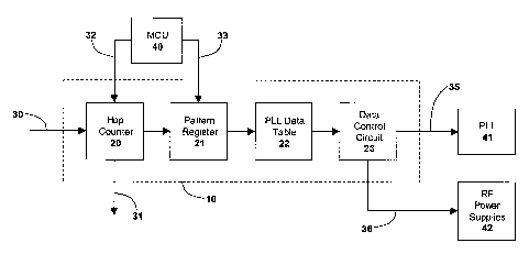
Fig. 1 is a schematic block diagram of one embodiment of the invention,
as implemented in a frequency hopping radio system with an external
microcontroller which sets the number of frequencies in the hop pattern, and
implements dynamic channel allocation, which embodiment also controls
auxiliary external circuits via dedicated control lines; and
Fig. 2 is a schematic block diagram of another embodiment of the
invention, as implemented in a frequency hopping radio system which also
allows an external microprocessor to override the default controller operation
and
program the PLL, which embodiment also controls auxiliary external circuits
via a
serial interface common to the PLL.
DETAILED DESCRIPTION OF THE INVENTION
While this invention is susceptible to embodiment in many different forms,
there are shown in the drawings and will be described in detail herein several
specific embodiments, with the understanding that the present disclosure is to
be
considered as an exemplification of the principle of the invention and is not
intended to limit the invention to embodiments illustrated.
Fig. 1 of the drawings illustrates an embodiment of the present invention
comprising a hardware-implemented phase-locked loop ("PLL") controller.
Specifically, the PLL controller utilizes an indirect addressing scheme to
access
PLL data for repeated programming of a PLL at a fixed rate according to a
specified sequence of tuning frequencies.
-5-
CA 02324839 2000-10-31
Fig. 1 is a schematic block diagram of the PLL controller 10, and the
interconnection between PLL controller 10 and related external circuitry,
including PLL 41 and optional microcontroller unit ("MCU") 40. PLL controller
10
is composed of hop counter 20, pattern register 21, PLL data table 22, and
data
control circuit 23.
Hop counter 20 includes a counter which increments its state at regular
periodic intervals. As commonly implemented in a frequency hopping radio
system, hop counter 20 will increment many times per second. When the state
of hop counter 20 reaches a maximum state, it is reset to zero and counting up
begins anew. The specified maximum state can either be predetermined, or can
be set by optional external MCU 40 via connection 32. Connection 32 will
generally consist of an electrical connection between MCU 40 and hop counter
whereby MCU 40 can program a maximum number of states for hop counter
15 20.
In some implementations, such as in systems with multiple transceivers,
hop counter 20 may include hop synchronization input 30 and hop
synchronization output 31. A signal applied to hop sync input 30 forceably
20 resets the hop counter state. Similarly, hop sync output 31 provides a
signal
after hop counter 20 reaches its maximum state. In a system with multiple
transceivers, hop sync output 31 of a first transceiver can be applied to hop
sync
input 30 of a second transceiver, thereby causing multiple transceivers to
step
through their respective hop sequences synchronously.
The aforementioned hop sequence synchronization between transceivers
can provide several advantages in a communications system involving one or
more portable units communicating with multiple base units. The advantages
stem from the fact that when hop sequences are synchronized throughout such
-6-
CA 02324839 2000-10-31
a system, any portable device can communicate with any base unit by simply
loading a common hop sequence. For example, in an office wireless telephone
environment, a pool of available base units can be dynamically allocated to
corresponding portable units based on portable unit demand, thereby enabling
system implementation with a reduced number of base units. Also, by providing
multiple base units dispersed throughout the system coverage area, a portable
unit need only transmit with sufficient power to be adequately received at the
nearest available base unit. The reduced transmission power increases portable
unit battery life, and reduces interference with other nearby devices
operating
simultaneously on the same frequency band. Furthermore, as a portable user
moves away from one base unit and towards another, the call can be seamiessly
"handed off' between base units without interruption by loading the portable
unit's hop sequence into the initiating base unit before ending the connection
with the terminating base unit.
Another feature of PLL controller 10 is that hop sequence synchronization
can easily be maintained during low-power "sleep mode" operation of a handset
transceiver. By maintaining power to only hop counter 20, hop counter 20 will
remain synchronized with other devices in the system, except to the extent
that
any frequency drift of the oscillator internal to hop counter 20 relative to
the other
devices causes inaccuracies. Other transmit and receive circuitry can
therefore
be de-powered when not needed to conserve power and maximize battery life.
Communications may resume immediately upon the transceiver awakening to
full power mode by limiting sleep periods to a length after which any slight
frequency drift that has occurred requires only bit alignment rather than a
complete sync reacquisition. The acceptable maximum sleep time will depend
upon the hop counter oscillator precision and transmission rate (or bit
period),
and can be determined by one of ordinary skill in the art.
-7-
CA 02324839 2000-10-31
The output of hop counter 20 is electrically connected to the address input
of pattern register 21. Pattern register 21 stores the frequency channel
numbers
comprising the hop sequence in consecutive memory locations. The output of
pattern register 21 therefore provides a frequency channel number to PLL data
table 22. Pattern register 21 may optionally include memory write port 33.
Memory write port 33 allows external circuitry, such as MCU 40, to change the
frequency channel contained in any given memory location of the pattern
register. Memory write port 33 therefore allows convenient implementation of
various dynamic channel allocation techniques. Dynamic channel allocation is
an advantageous feature of frequency-hopping radios whereby the effects of
fixed-frequency sources of interference or channel degradation can be avoided
by removing the frequency upon which communications are impaired from the
hop sequence, and replacing it with a new frequency. When interference on the
new frequency is less than that on the channel which it replaced, the overall
quality of the communications link has been improved. Channel evaluations and
allocation decisions are made by MCU 40 in the embodiment illustrated. Several
dynamic channel allocation methods are known in the art.
PLL data table 22 contains the PLL command words necessary to
program the PLL to each frequency channel. It outputs the command words
which program PLL 41 to the frequency indicated by the channel number
received from the pattern register. The exact content of the command words
will
depend upon the design and programming model of the particular PLL utilized,
as is known by one of ordinary skill in the art.
The output of PLL data table 22 is electrically connected to data control
circuit 23, which actually programs the phase-locked loop device 41 via
interface
35. Data control circuit 23 performs the format conversions and implements the
programming interface required by the PLL 41 programming protocol. For
-8-
CA 02324839 2000-10-31
example, many phase-locked loop devices are programmed via a serial
programming interface, in which case the data control circuit includes a
parallel
to serial converter, and synthesizes clock and frame signals for transmission
via
interface 35.
Wireless communication devices commonly include both transmitter and
receiver circuits. Accordingly, the present invention could be utilized by one
of
ordinary skill in the art in numerous embodiments to control both transmit and
receive PLLs. For example, in an embodiment in which transmit and receive
communications are time domain duplexed, and a single PLL is utilized for both
transmit and receive circuits, the output of PLL data table 22 may include
both
transmit and receive PLL programming words. Data control circuit 23 then
sequentially programs PLL 41 to the transmit and receive frequencies.
Alternatively, if separate PLLs are utilized for transmit and receive
circuits, an
embodiment of the invention may be utilized which incorporates parallel
receive
and transmit PLL data tables and data control circuits, such that each PLL is
driven by a common hop counter and pattern register, but programmed by
separate data tables and control circuits. Such alternative embodiments are
within the scope of this invention, inasmuch as they would be known to one of
skill in the art in view of the disclosure provided herein.
Additionally, data control circuit 23 optionally provides signals to control
miscellaneous aspects of RF circuit functionality. For example, it may be
desirable to de-power a transmitter and/or receiver during periods of nonuse
to
conserve power and prolong battery life. Furthermore, t is often desirable to
de-
power a transmitter while the PLL is changing frequencies, so as to avoid
unwanted energy transmission on spurious frequencies during the PLL tuning
acquisition. In such example, data control circuit 23 may include
miscellaneous
control line 36 connected to RF circuit power supplies 42 as depicted in Fig.
1.
-9-
CA 02324839 2000-10-31
Data control circuit 23 may then assert line 36 to deactivate supplies 42,
thereby
turning off the transmitter, before programming PLL 41 with a new tuning.
Control circuit 23 can then de-assert line 36 to reactivate supplies 42 after
the
PLL has locked on to the new frequency, thereby resuming transmission at the
new frequency. Fig. 2 illustrates an alternative embodiment in which external
power supplies 42 are a node on a common serial programming interface 35, in
which case supplies 42 are addressed and controlled via serial commands from
data control circuit 23.
Finally, data control circuit 23 may optionally include an overriding input
34, as depicted in Fig. 2. Override input 34 allows external circuit MCU 40 to
directly control the output of data control circuit 23, regardless of commands
received from PLL data table 22. This feature can be used, for example, to
send
initialization commands to PLL 41 upon device power-up, or for providing a
diagnostic test mode of PLL operation.
The foregoing description and drawings merely explain and illustrate the
invention and the invention is not limited thereto except insofar as the
appended
claims are so limited, inasmuch as those skilled in the art, having the
present
disclosure before them will be able to make modifications and variations
therein
without departing from the scope of the invention.
-10-