Note: Descriptions are shown in the official language in which they were submitted.
CA 02325148 2000-11-06
The invention relates to a device to carry electric current and conduct heat.
Especially
devices for high electric current applications, where there is a strong need
to evacuate
heat generated in electronic or electric components.
In the prior art, high current conductors are shown mixed in a printed circuit
board
together with low signal conductors. See, for example, US 5,223,676
(Yamamoto), US
4,446,188 (Patel et. al).
The use of an embedded heat sink is shown in US 4,866,571 (Butt), using a
separate
electric conductor to connect to a semiconductor mounted onto the heat sink.
The prior art has the apparent drawback of not providing a flexible (easily
adaptable to
different product requirements) current conducting system which provides
adequate
heat transfer from the heat generating components.
It is an object of the invention to provide a device which carries electronic
and electric
components, supplies them with a plurality of high current electric flows and
conducts
the heat generated in the components away from the components themselves, and
accomplishes these tasks using a minimum of space and in a non-complicated
mechanical arrangement. The manufacture of the device according to the
invention is
possible in existing production lines, without any alteration of the
manufacturing
machines.
In the invention, a basic "sandwich" structure is used, capable of efficient
heat transfer
and high current carrying capacity. The structure is capable of forming a
power circuit
with multiple current paths.
The multiple current path device, for carrying electric current to and
conducting heat
from an electronic circuit, according to the invention preferably has the
following
components:
a heat sink,
-1-
CA 02325148 2000-11-06
a plurality of electrically and thermally conducting substrates forming
several,
from each other electrically insulated, current conductors,
a thermally conductive, electrically insulating first layer, bonding each
conducting
substrate and the heat sink, and
a plurality of electronic or electric components electrically and thermally
connected to the conducting substrates.
The device preferably further comprises a plurality of printed circuits
arranged on any
of the conducting substrates, each printed circuit being electrically
insulated from the
conducting substrate. The device further advantageously comprises a plurality
of
thermally conductive, electrically insulating second layers bonding the
conducting
substrate and the individual printed circuits. Still further, the conducting
substrates may
have electrically conductive vias, which conduct current between said
conducting
substrates and said printed circuits.
Each individual electronic or electric components is advantageously fastened
on one
individual conducting substrate, or may bridge two or more conducting
substrates ortwo
or more printed circuits. Alternatively, each individual electronic or
electric components
may be fastened to bridge one printed circuit and one conducting substrate.
The conducting substrates are preferably substantially flat and rectangular.
The device according to the invention preferably comprises two, three, four or
five
conducting substrates.
Each of said conducting substrates may preferably have a power connection, for
connecting to a current carrier. The power connection may be a bolt means or
be a
protrusion of the conducting substrate itself.
The device according to the invention may preferably be a half bridge electric
power
circuit, a full bridge electric power circuit or a 3-phase bridge electric
power circuit.
-2-
CA 02325148 2000-11-06
A further embodiment of the device according to the invention further
comprises a
substantially thermally insulating fibre-glass reinforced resin board, bonded
to the
thermally conductive, electrically insulating first layer with the use of an
adhesive layer
and is electrically connected to the plurality of electrically and thermally
conducting
substrates via one or more of the electronic components. The resin board
preferably
has one or more layers of printed circuit patterns electrically connected to
the electric
components.
In order that the invention may be more clearly understood, the preferred
embodiment
thereof will now be described in detail by way of example, with reference to
the
accompanying drawings, in which:
Fig. 1 A is a schematic top view of a device according to the invention
showing three
conducting substrates with a common heat sink and the associated
components,
Fig. 18 is a schematic sectional side view along line A-A of Fig. 1 A,
Fig. 2A is a schematic diagram of the heat dissipation mechanism of a device
according to the invention,
Fig. 2B is a schematic diagram of the thermal resistance from case to sink for
a
cased electronic component,
Fig. 3A is a schematic top view of a half-bridge device according to the
invention,
Fig. 3B is a schematic electric diagram of the device according to Fig. 3A,
Fig. 4A is a schematic top view of a full-bridge device according to the
invention,
Fig. 4B is a schematic electric diagram of the device according to Fig. 4A,
-3-
CA 02325148 2000-11-06
Fig. 5A is a schematic top view of a phase-bridge device according to the
invention,
Fig. 5B is a schematic electric diagram of the device according to Fig. 5A,
Fig. 6 is a schematic top view of a board fixture according to the invention,
Fig. 7 is a schematic elevational side view of the fixture according to Fig.
6, but
without individual substrates, i.e. an empty fixture,
Fig. 8A is a schematic top view of a further embodiment of a device according
to the
invention, and
Fig. 8B is a schematic sectional side view along line B-B of Fig. 8A.
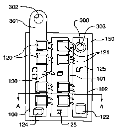
Figs. 1 A, 1 B and 3A show an embodiment of the invention having three
electrically and
thermally conducting substrates 100, 101, 102 arranged side-by-side on a
common
heat sink 200. The heat sink is preferably made of aluminum.
The invention is not limited to three substrates, any number of conducting
substrates
may be used, the number being determined by the number of separate current
flows
used in a particular application. Preferably, two, three, four orfive
conducting substrates
are used. The preferred material for the conducting substrates is copper, but
any
conducting material may be used, such as any metal, metal alloy or semi-
conductor.
The conducting substrates may have an arbitrary shape, but a generally flat
configuration having a contoured edge is preferred. For instance,
substantially flat and
rectangular, elliptical or round shapes are useful. Alternatively, any number
of
protrusions or indentations in the contour may be used, depending upon the
application,
for example to connect components between one or more conductive substrates.
A thermally conductive, electrically insulating first layer 150 is arranged
between the
conducting substrates 100,101, 102 and the heat sink 200, to provide a bond
between
them. For applications where the power dissipation is relatively low, the
substrates
-4-
CA 02325148 2000-11-06
themselves act as sufficient cooling means, thus the heat sink 200 and the
thermally
conductive, electrically insulating first layer 150 may be omitted for these
applications.
For higher power dissipation applications, the heat sink is necessary. Onto
each
conducting substrate individual printed circuits 170 optionally may be
fastened,
preferably via a thermally conductive, electrically insulating second layer
160, as is
shown in Fig. 1 B on the middle substrate 101. Optionally, further printed
circuits may
be affixed onto printed circuits already fastened to the conducting substrate,
thus
creating a multilayer printed circuit structure, as is shown in Fig. 1 B on
the rightmost
substrate 102. Each additional printed circuit would preferably be mounted to
an earlier
printed circuit with the thermally conductive, electrically insulating second
layer 160
there-between. The shape of the printed circuits is either the same as the
shape of the
conducting substrates, or any desirable shape which fits within the contour of
the
substrate.
Electric or electronic components 120, 121, 124, 125 are soldered or otherwise
connected to the circuit pattern on each printed circuit, for example via a
bonding layer
123. The components may also be embedded into a multilayer printed circuit, as
is
already known. Alternatively, embedded components may be used with a one-layer
printed circuit pattern together with multiple insulating layers to cover the
component.
Examples of components are electronic switches, diodes, resistors and MOSFETs
of
different types. Electrically conductive vias 180 are arranged to connect each
individual
conducting substrate 100,101,102 to those printed circuits which are connected
to that
particular substrate. The vias conduct electricity between the conducting
substrate and
the printed circuits. The components may be mounted either directly to a
substrate, as
is shown in Fig. 1 B on the leftmost substrate 100, or directly to an
insulating second
layer 160. In either case, the heat generated by the component will be led
into the
substrate and further to the heat sink. The substrates andlor printed circuits
may also
be electrically connected by inter-substrate connections 130.
The heat sink 200 may have fins 210 for added efficiency. The heat sink may
preferably
be used as one or more walls of an enclosure for the device (not shown). A lid
(not
shown) having a top portion and two side portions, will effectively enclose
the
-5-
CA 02325148 2000-11-06
electronics mounted on the device. The shape and size of the heat sink is
governed by
the amount of heat that has to be transported from the device. Components 120
may
be soldered, or otherwise electrically connected to the printed circuits or
directly to the
substrates 100, 101, 102 to reach between two printed circuits mounted onto
two
different conducting substrates 100, 101, 102 or reach between two substrates
or
between a printed circuit and a substrate. Power connections to the conducting
substrates may be realized as a self-clinching bolt 300 having a threaded
connector
portion 303, or by making the conducting substrates themselves have a
protrusion 301
with mounting holes 302. The protrusions would reach out from the final
package, to act
as terminals.
The same general buildup of the sandwich lends itself to applications such as
VLSI,
bare die and hybrid modules construction. As long as the heat generating
components
can be mounted to the substrates or the second insulating layers in a way to
ensure
sufficient heat transfer, any type of component is envisioned to be used with
the device
according to the invention.
The multiple current path device, for carrying electric heat and conducting
heat from an
electronic circuit, according to the invention, has great advantages in the
area of
combined heat conducting and electric current conducting capabilities. The
junction
temperature, i.e. the temperature at the core or die of the component, is
determined by
the power dissipation of the component and the thermal resistances. The desire
is to
keep this junction temperature below a certain maximum temperature, which
depends
on the component used. In general, the junction temperature of a device in
steady state
can be expressed as (see Fig. 2A):
Tjunction - PD ( RBJC + RACS + RASA) + Tambient
Where
PD = power dissipation of the component,
Re~c = Thermal resistance from junction to case
Recs = Thermal resistance from case to sink
-6-
CA 02325148 2000-11-06
ResA = Thermal resistance from sink to ambient
T;u~~,~~, = junction temperature
Tambient = Ambient temperature
An important goal, as mentioned above, is to minimize the junction temperature
to
reduce stress on the component and make the design more robust. In addition,
lower
average junction temperature in semiconductor switches generally leads to
longer
component lifetimes. Finally, in designs in which multiple positive
temperature
coefficient devices are parallelled (eg. MOSFETs) the sharing between the
components
is improved with lower thermal drops between components. Re~c, being the
thermal
resistance from junction to case, is a device parameter over which the circuit
designer
has no control. However, Recs and Reso, are parameters which are controlled by
the
designer. ResA can be minimized by selecting a larger heat sink for conductive
cooling
or improving surface area and air velocity for convective cooling. Recs can be
reduced
by using clever approaches to mounting the devices. Typically, this thermal
resistance
can be quite large resulting from the electrically insulating material placed
between the
package of the components and the heat sink, and will vary with material
thickness and
mounting pressure.
In the invention, the thermal resistance from case to sink, Rocs, is split
into two small
series components: the thermal resistance from the component case to the
conducting
substrate (Rec-c~) and the thermal resistance from the conducting substrate to
the heat
sink (Racu.$), as shown in Fig. 2B. The R~~~ thermal resistance is extremely
small since
it will normally be directly connected with solid conducting vias from the top
printed
circuit layer to the conducting substrate. The Rec~-s thermal resistance is
also extremely
small since the area between the conducting substrate and the heat sink is
quite large.
Generally, thermal resistance has the following relationship:
Re ~ 1 I (Area)
The effective area of dissipation through the insulating material thus
effectively "heat-
spreads" from an area on the order of the size of the device to the area of
the
-7-
CA 02325148 2000-11-06
conducting substrate. The conducting substrate can be made large and hence the
thermal resistance can be dramatically lowered.
The device according to the invention also has transient thermal impedance
advantages. The heat capacity of the conducting substrate is quite large
compared to
a single component. Also, the thermal resistance R~_~~ is quite small (as
described
above). Therefore, the components now have a low resistance thermal path to a
large
heat capacitance resulting in a greatly improved transient thermal impedance.
This
results in a more rugged design capable of withstanding a higher peak power
dissipation and higher peak currents.
Typically, electric resistance is expressed as:
R = (length) / (p ~ Area)
Where p is conductivity (a property of the material). A substrate comprising a
conductor,
such as copper, with a low resistivity is capable of carrying very large
currents. The
current handling capability of the conducting substrate can be increased
arbitrarily by
simply using a thicker substrate and/or increasing the width of the substrate.
Also, this
approach is well suited for conducting high frequency signals since the skin-
effect is
reduced by the intrinsically large surface area of the conducting substrate
conductor.
With judicious layout of the relative positions of the conducting substrates,
the effective
loop areas and hence inductance may also be kept to a minimum.
The invention may have different embodiments, apparent to the person skilled
in the
art after learning the inventive concept:
- The conducting substrate "islands" may be of arbitrary shape.
- The number of conducting substrate "islands" is not fixed. Typically there
will be one
distinct conducting substrate for every high-current node in the circuit.
- The number of layers on the printed circuit is not limited to one. A single
layer is,
however, most cost effective.
_g_
CA 02325148 2000-11-06
- The heat sink may not be a distinct mechanical part (added for the sole
purpose of
being a heat sink), but may actually be a structural part of the machine being
controlled, for example the casing of an electric motor. The device according
to the
invention could then be placed either inside or outside on the motor casing.
- The heat sink may be flat for conductive cooling mounting or provided with
fins for
convective cooling.
- The conducting substrates may be arranged in a non-flat configuration, for
example
three substrates may be arranged in a triangular cross-section. This would
simplify
cross-connections between substrates.
Devices according to the invention can be used to realize:
- A 112 bridge configuration on a sandwich as shown, using only one single
layer of
printed circuit.
- 3-phase bridge topology.
- Any power circuit wherein the high current conducting paths/nodes each form
a
conducting substrate.
A half bridge device according to the invention is shown in Fig. 3A. The
electric diagram
of this device is shown in Fig. 3B. The three substrates have different tasks:
a positive
supply substrate 100, a ground substrate 102 and an output substrate 101. Hi-
side
switches 145 connect the positive supply substrate and the output substrate
and Lo-
side switches 146 connect the ground substrate and the output substrate.
Decoupling
capacitors 140 connect the positive substrate and the ground substrate. The
substrates
are mounted on a heat sink 200 as described earlier. The switches are single
or parallel
devices, e.g. MOSFETs.
A full bridge device according to the invention is shown in Fig. 4A. The
electric diagram
of this device is shown in Fig. 4B. The four substrates have different tasks:
a positive
supply substrate 100, a ground substrate 102 and an output substrate split
into a first
output substrate 101' and a second output substrate 101 ". A first set of Hi-
side switches
145' connect the positive supply substrate and the first output substrate, and
a second
set of Hi-side switches 145" connect the positive supply substrate and the
second
_g_
CA 02325148 2000-11-06
output substrate. Similarly, a first set of Lo-side switches 146' connect the
ground
substrate and the first output substrate, and a second set of Lo-side switches
146"
connect the ground substrate and the second output substrate. Decoupling
capacitors
140 connect the positive substrate and the ground substrate. The substrates
are
mounted on a heat sink 200 as described earlier. The switches are single or
parallel
devices, e.g. MOSFETs.
A phase bridge device according to the invention is shown in Fig. 5A. The
electric
diagram of this device is shown in Fig. 5B. The five substrates have different
tasks: a
positive supply substrate 100, a ground substrate 102 and an output substrate
split into
a first phase output substrate 101', a second phase output substrate 101" and
a third
phase output substrate 101 "'. A first set of Hi-side switches 145' connect
the positive
supply substrate and the first output substrate, a second set of Hi-side
switches 145"
connect the positive supply substrate and the second output substrate, and a
third set
of Hi-side switches 145"' connect the positive supply substrate and the third
output
substrate. Similarly, a first set of Lo-side switches 148' connect the ground
substrate
and the first output substrate, a second set of Lo-side switches 146" connect
the
ground substrate and the second output substrate, and a third set of Lo-side
switches
146"' connect the positive supply substrate and the third output substrate.
Decoupling
capacitors 140 connect the positive substrate and the ground substrate. The
substrates
are mounted on a heat sink 200 as described earlier. The switches are single
or parallel
devices, e.g. MOSFETs.
Many applications would benefit from this approach including:
- Motor controllers including
electric vehicle motor controllers
robot controllers
linear motor drives
- Power converters
resonant converters
inverters (dclac)
dcldc converters
-10-
CA 02325148 2000-11-06
aclac converters
controlled acldc converters
voltagelcurrent regulators
- Loads
dummy active loads
over-voltage clamps
The method of manufacturing the device according to the invention, requires no
costly,
specialized tools. The majority ofthe construction may be achieved using
standard SMT
assembly machinery. The multiple conducting substrates are preferably jigged
to
appear as one single substrate to the machinery. An embodiment of a single
board
framing means 400 (or jig) is shown in Figs. 6 and 7. The jig has two short
sides 401
and two long sides 402, together with a bottom 407. A plurality of
compartments 403,
404, 405, 406 are arranged in the jig, separated by partition walls 408. Each
compartment is deep enough to allow the upper surface of an inserted substrate
to be
substantially flush with the upper surface of the jig 400.
The example shown is a jig to hold substrates corresponding to the substrates
of Fig.
4A: a positive supply substrate 100, a ground substrate 102 and an output
substrate
split into a first output substrate 101' and a second output substrate 101 ".
The
substrates are placed in the jig and the jig inserted into existing board
manufacturing
machines, where the components 120, 121 are mounted in their desired locations
on
the substrates. This results in the ability to use existing machines for
building boards
and no complex or costly fixtures or additional machinery is required. The
multiple
conducting substrates are simply arranged on the simple and cheap "substrate
carrier"
Qig 400) and then placed through the standard SMT pick-and-place and re-flow
processes. One final additional step is attaching the finalized populated
conducting
substrate assembly to the heat sink.
Alternative embodiments of jigs are also useful. For example, a perforated
base board
having a multitude of holes may be used in conjunction with pegs inserted in
desired
locations on the base board, to form holders for individual substrates.
-11-
CA 02325148 2000-11-06
The assembly method of a device according to the invention thus preferably
comprises
the following steps:
- Use of a "substrate holder" jig to register and hold multiple conducting
substrates
as one board.
- Placement of electroniclelectric components using standard pick and place
machinery.
- Standard SMT re-flow soldering through a standard oven, the temperature
profile
may need some modification due to increased heat capacity of the conducting
substrates.
- Standard testing using flying probes or equivalent techniques.
- Optionally bonding conducting substrate assemblies to a heat sink.
- Final mechanical assembly
Power connections to the conducting substrate may be realized using self-
clinching
bolts or by allowing the conducting substrates themselves to protrude from the
final
package to act as "bus bar terminals". The heat sink may comprise all or part
of the
mechanical package.
Figs. 8A and 8B show a further embodiment of the invention having two
conducting
substrates 100,101 arranged side-by-side on the common heat sink 200. The
thermally
conductive, electrically insulating first layer 150 is arranged between the
conducting
substrates 100, 101 and the heat sink 200, to provide a bond between them. A
standard fibre-glass reinforced resin board 500, having one or more layers of
printed
circuits patterns is utilized as the "third substrate". The resin board is
substantially
thermally insulating, since no heat dissipating components are bonded to the
resin
board for cooling purposes. The resin board 500 is preferably bonded to the
thermally
conductive, electrically insulating first layer 150 with the use of an
adhesive layer 510.
Further reference numerals are identical to those previously used, and
designate the
same technical features as described above.
It will be appreciated that the above description relates to the preferred
embodiments
by way of example only. Many variations on the invention will be obvious to
those
-12-
CA 02325148 2000-11-06
knowledgeable in the field, and such obvious variations are within the scope
of the
invention as described and claimed, whether or not expressly described.
-13-