Language selection

Search

Patent 2326088 Summary

Third-party information liability

Some of the information on this Web page has been provided by external sources. The Government of Canada is not responsible for the accuracy, reliability or currency of the information supplied by external sources. Users wishing to rely upon this information should consult directly with the source of the information. Content provided by external sources is not subject to official languages, privacy and accessibility requirements.

Claims and Abstract availability

Any discrepancies in the text and image of the Claims and Abstract are due to differing posting times. Text of the Claims and Abstract are posted:

  • At the time the application is open to public inspection;
  • At the time of issue of the patent (grant).
(12) Patent: (11) CA 2326088
(54) English Title: COMPACT DIFFRACTION GRATING BASED WDM DEMUX
(54) French Title: DEMULTIPLEXEUR WDM A RESEAU DE DIFFRACTION COMPACT
Status: Expired and beyond the Period of Reversal
Bibliographic Data
(51) International Patent Classification (IPC):
  • G02B 6/26 (2006.01)
  • G02B 6/293 (2006.01)
  • G02B 6/34 (2006.01)
  • G02B 27/10 (2006.01)
  • H04J 14/02 (2006.01)
(72) Inventors :
  • DUCELLIER, THOMAS (Canada)
(73) Owners :
  • JDS UNIPHASE INC.
(71) Applicants :
  • JDS UNIPHASE INC. (Canada)
(74) Agent:
(74) Associate agent:
(45) Issued: 2006-01-24
(22) Filed Date: 2000-11-16
(41) Open to Public Inspection: 2001-06-22
Examination requested: 2002-07-22
Availability of licence: N/A
Dedicated to the Public: N/A
(25) Language of filing: English

Patent Cooperation Treaty (PCT): No

(30) Application Priority Data:
Application No. Country/Territory Date
60/171,456 (United States of America) 1999-12-22

Abstracts

English Abstract


In the area of wavelength division multiplexing (WDM), the present invention
relates to a demultiplexer/multiplexer based on a diffraction grating, in
which a beam of
light is separated into two orthogonally polarized sub-beams prior to beam
collimation.
Due to the characteristics of the beam splitting crystal, parts of the sub-
beams overlap
resulting in portions of the sub-beams becoming improperly polarized. Too
alleviate the
errors cause thereby, an iris is placed over the diffraction grating to
eliminate the portions
of the light that have been polarized improperly.


Claims

Note: Claims are shown in the official language in which they were submitted.

We Claim:
1. A wavelength division demultiplexer device comprising:
an input waveguide for launching an input multiplexed light beam into the
device:
polarization beam splitting means for separating the input light beam into two
polarized sub-beams;
first polarization rotating means for rotating one of the two sub-beams to
provide
two parallel polarized sub-beams, wherein a portion of one of the sub-beams is
not properly polarized;
light collimating means for collimating the two parallel sub-beams;
diffraction grating means for separating the two sub-beam into a first and a
second plurality of output light sub-beams; and
light blocking means in front of the diffraction grating for eliminating at
least
some of the portion of one of the sub-beams not properly polarized.
2. The device according to claim 1, further comprising:
light focussing means for focussing the first and second plurality of output
light
sub-beams;
second polarization rotating means for rotating one of the plurality of sub-
beams
to provide two orthogonal pluralities of sub-beams;
polarization beam combining means for combining the two orthogonal pluralities
of sub-beams into a plurality of output light beams; and
a plurality of waveguides for receiving the plurality of output light beams.
3. The device according to claim 2, wherein the diffraction grating means is
adapted
to reflect the first and second plurality of sub-beams back parallel to the
input sub-beams.
whereby the light collimating means is also the light focussing means, the
first
polarization means is also the second polarization means, and the polarization
beams
splitting means is also the polarization beam combining means.
4. The device according to claim 1, wherein the light-blocking means is an
iris.
6

5. The device according to claim 1, wherein the diffraction grating means is
arranged whereby the two sub-beams are image superimposed thereon.
6. The device according to claim 5, wherein portions of both of the sub-beams
are
not properly polarized, and wherein the light blocking means is annular for
eliminating at
least some of the portions of the sub-beams that are not properly polarized.
7. The device according to claim 1, wherein the polarization beam splitting
means is
a birefringent crystal.
8. The device according to claim 1, wherein the first polarization rotating
means is a
half-wave plate.
9. The device according to claim 1, wherein the light collimating means is a
grin
lens.
10. The device according to claim 1, wherein the light blocking means is
adapted to
ensure that a zero in a diffraction pattern thereof falls on a neighboring
output channel.
7

Description

Note: Descriptions are shown in the official language in which they were submitted.


CA 02326088 2000-11-16
Doc. No. 10-314 CA Patent
COMPACT DIFFRACTION GRATING BASED WDM DEMUX
The present invention relates to multiplexing and demultiplexing optical
signals,
and in particular to a diffraction grating based wavelength
multiplexer/demultiplexer.
BACKGROUND OF THE INVENTION
Fiber optic telecommunications rely nowadays on a technique called "DWDM"
(dense wavelength division multiplexing) to achieve higher bandwidth at lower
cost. This
technique utilizes many different wavelength bands each carrying an
independent channel
of information. These wavelengths usually span a 50 nm band in the 1.55 ~m
region. The
ITU has normalized these wavelengths to lie on a periodic frequency grid with
a spacing
of typically 100 to 200 GHz. The present invention relates to a wavelength
demultiplexer. This is a special kind of optical filter having one input
receiving the
wavelength multiplexed channels and several outputs each receiving the
separated
wavelength channels. U.S. Patent Nos. 4,111,524; 4,198,117; 4,522,462 and
4,763,969
disclose typical WDM devices. It should be noted that everything that is
stated in this
disclosure relates both to demultiplexers (1 input and N outputs) and
multiplexers (N
inputs and 1 output), which are the same devices with the inputs and the
outputs reversed.
A typical realization of a diffraction grating based dense WDM wavelength
demultiplexer is illustrated in figure 1. The typical diffraction grating
demultiplexer
includes: coupling optics 1, which can be as simple as the optical fibers
themselves, or
include an array of micro lenses (as in European Patent EP 0859249A1);
collimating
optics 2, which can be one or more lenses, or a curved mirror (on which the
grating can
be directly written if needed); and a diffraction grating 3.
The most compact configuration is called the Littrow configuration, where the
reflected output beams from the grating are almost aligned with the input beam
(like in
Fig. l ).
In order to achieve sufficient wavelength separation in the focal plane, the
device
must have a high dispersion. This is either done using a large focal length
lens or using a

CA 02326088 2000-11-16
Doc. No. 10-314 CA Patent
high groove frequency grating. However, diffraction gratings suffer from
polarization
sensitivity when the groove frequency is above ca. 600 lines/mm. This implies
that the
focal length of the lens should be at least 20mm for 200 CrHz spacing.
Another approach is to use higher groove frequency grating in conjunction with
some polarization processing to maintain low polarization sensitivity. This is
described
for example in US Patents Nos. 4,741,588, issued May 3, 1988 to Antonius Nicia
et al,
and 5,886,785, issued March 23, 1999 to Herve Lefevre et al. The polarization
processing
used in these patents is done when the beams are collimated (see figure 2).
The main purpose of the polarization diversity technique is to convert input
light
into two sub-beams with the same polarization state, the one that has the
highest
diffraction efficiency from the grating (usually at 1.55 Vim, it is a linear
polarization
perpendicular to the grating's grooves). This is achieved through the
combination of a
polarization splitting device 4, usually splitting input light into two
perpendicular linear
states of polarization 6 and 7 parallel and perpendicular to the grating
lines, and a
waveplate 8. The polarization splitting device 4 is either a polarization beam
splitter or a
birefringent beam displacer. The waveplate 8 is usually a single half wave
plate oriented
at 45° with respect to the groove axis positioned in the path of one of
the two sub-beams.
The main drawback of this technique is that since it is done with the
collimated
beams, which have relatively large diameters, this polarization-processing
scheme is
bulky.
SUMMARY OF THE INVENTION
An object of the present invention is to overcome the shortcomings of the
prior art
by providing a diffraction grating based WDM in which the polarization
processing is
executed prior to collimation.
Accordingly, the present invention relates to a wavelength division
demultiplexer
device comprising:
an input waveguide for launching an input multiplexed light beam into the
device;
polarization beam splitting means for separating the input light beam into two
polarized sub-beams;
2

CA 02326088 2000-11-16
Doc. No. l0-314 CA Patent
first polarization rotating means for rotating one of the two sub-beams to
provide
two parallel polarized sub-beam, wherein a portion of one of the sub-beams is
not
properly polarized;
light collimating means for collimating the two parallel sub-beams;
diffraction grating means for separating the two sub-beam into a first and a
second plurality of output light sub-beams; and
light blocking means in front of the diffraction grating for eliminating at
least
some of the portion of one of the sub-beams not properly polarized.
BRIEF DESCRIPTION OF THE DRAWINGS
The invention will be described in greater detail with reference to the
accompanying drawings which represent a preferred embodiment of the invention
and
wherein:
Figure 1 is a schematic drawing illustrating a typical diffraction grating
based
WDM device;
Figure 2 is a schematic drawing illustrating a typical diffraction grating
based
WDM device with polarization diversity;
Figure 3 is a schematic drawing illustrating the diffraction grating based WDM
device according to the present invention; and
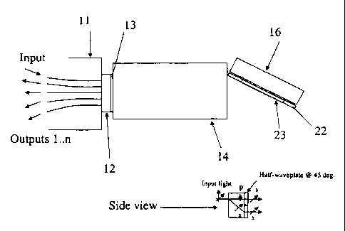
Figure 4 is a schematic drawing illustrating the WDM device of Figure 3.
DETAILED DESCRIPTION OF THE INVENTION
With reference to Figures 3 and 4, the WDM of the present invention, is a very
compact diffraction grating based wavelength demultiplexer for 200 GHz channel
spacing including an input waveguide chip 11 supporting one input and N
outputs, a
polarization beam splitting element 12, a polarization rotator 13, a GRIN lens
14 as the
collimating lens, and a high frequency groove grating 16. The polarization
processing
technique is in the focal plane to lower the polarization sensitivity of the
device (see
figure 3).
3

CA 02326088 2000-11-16
Doc. No. 10-314 CA Patent
More specifically, the diffraction grating 16 has 1200 l/mm, the GRIN lens 14
is
an almost quarter pitch SLW3.0 from NSG, and the waveguide coupling scheme 11
(with
about 21 microns between waveguides) are used to achieve 200 GHz channel
spacing.
The polarization processing technique is done in front of the collimating lens
14 and uses
a rutile element 12 of 1 mm thickness. The rutile 12 is oriented in such a way
as to
separate the input light into two sub-beams 17 and 18 with s and p linear
polarizations,
respectively. A half wave plate 13 covers the p-polarized sub-beam to convert
it into s
polarization (see Fig. 4). This way, all the input light is converted into s
polarization,
which has the highest diffraction efficiency.
However, with normal fiber, the polarization walk-off induced by ruble is too
small. Therefore, the diverging beams emerging from the rutile 12 overlap.
This will
cause some of the input light not to be converted into s polarization (the
part 19 of the p
sub-beam 18 that will not traverse the waveplate). Furthermore this
arrangement results
in some of the input light to be improperly converted to p polarization (the
part 20 of the
s sub-beam 17 that will see the waveplate). This will result in unwanted
polarization
dependent loss.
To alleviate this polarization-overlapping problem, a light blocking plate,
preferably in the form of an iris 22, is positioned on top of the grating 16
forming an
aperture 23. In a preferred embodiment a special optical arrangement is used
in which the
two sub-beams 17 and 18 emerging from the rutilel2 are imaged superimposed on
the
grating 16 forming superimposed beam 24. This is easily achieved if the
optical length
from the waveguide 11 to the input facet of the Grin lens 14 is the same as
the optical
length from the output facet of the Grin lens 14 to the grating I 6. The
polarization
overlapping parts 19 and 20 of the sub-beams are imaged on the grating 16 as
the top and
bottom portions 25 of the superimposed beam 24 (see fig.4). Therefore, when
the iris 22
is put on top of the grating 16, it can effectively eliminate the top and
bottom parts 25 of
the beam, and the polarization overlap will be removed. The effect of the iris
22 can also
be described as a limitation of the input numerical aperture (NA), at the
expense of
increased loss.
The advantages of using an iris 22 on top of the grating 16 include:
4

CA 02326088 2000-11-16
Doc. No. 10-314 CA Patent
reduces the input NA of the sub-beams 17 and I 8 to increase polarization
splitting from
the rutile 12 at the expense of additional losses;
reduces the input NA of sub-beams 17 and 18, therefore lowering the spherical
aberrations in the Grin lens 14;
creates an appropriate Fourier filter to enhance the channel bandwidth and
lower the
optical crosstalk (this is achieved when a diffracted Airy disk from the iris
22 is chosen
such that the first dark ring falls on the neighboring channel).

Representative Drawing
A single figure which represents the drawing illustrating the invention.
Administrative Status

2024-08-01:As part of the Next Generation Patents (NGP) transition, the Canadian Patents Database (CPD) now contains a more detailed Event History, which replicates the Event Log of our new back-office solution.

Please note that "Inactive:" events refers to events no longer in use in our new back-office solution.

For a clearer understanding of the status of the application/patent presented on this page, the site Disclaimer , as well as the definitions for Patent , Event History , Maintenance Fee  and Payment History  should be consulted.

Event History

Description Date
Revocation of Agent Requirements Determined Compliant 2020-09-01
Time Limit for Reversal Expired 2010-11-16
Inactive: Adhoc Request Documented 2010-02-11
Letter Sent 2009-11-16
Letter Sent 2009-01-16
Inactive: Office letter 2008-12-02
Grant by Issuance 2006-01-24
Inactive: Cover page published 2006-01-23
Pre-grant 2005-11-10
Inactive: Final fee received 2005-11-10
Notice of Allowance is Issued 2005-10-03
Letter Sent 2005-10-03
Notice of Allowance is Issued 2005-10-03
Inactive: Approved for allowance (AFA) 2005-09-09
Inactive: IPC assigned 2004-12-03
Inactive: First IPC assigned 2004-12-03
Inactive: IPC assigned 2004-12-03
Inactive: Office letter 2003-09-10
Revocation of Agent Requirements Determined Compliant 2003-09-10
Inactive: Office letter 2003-09-09
Revocation of Agent Request 2003-07-22
Letter Sent 2002-08-28
Amendment Received - Voluntary Amendment 2002-07-22
Request for Examination Requirements Determined Compliant 2002-07-22
All Requirements for Examination Determined Compliant 2002-07-22
Request for Examination Received 2002-07-22
Application Published (Open to Public Inspection) 2001-06-22
Inactive: Cover page published 2001-06-22
Inactive: First IPC assigned 2001-01-31
Letter Sent 2001-01-05
Inactive: Filing certificate - No RFE (English) 2001-01-05
Filing Requirements Determined Compliant 2001-01-05
Inactive: Inventor deleted 2001-01-02
Application Received - Regular National 2001-01-02

Abandonment History

There is no abandonment history.

Maintenance Fee

The last payment was received on 2005-10-27

Note : If the full payment has not been received on or before the date indicated, a further fee may be required which may be one of the following

  • the reinstatement fee;
  • the late payment fee; or
  • additional fee to reverse deemed expiry.

Please refer to the CIPO Patent Fees web page to see all current fee amounts.

Owners on Record

Note: Records showing the ownership history in alphabetical order.

Current Owners on Record
JDS UNIPHASE INC.
Past Owners on Record
THOMAS DUCELLIER
Past Owners that do not appear in the "Owners on Record" listing will appear in other documentation within the application.
Documents

To view selected files, please enter reCAPTCHA code :


To view images, click a link in the Document Description column. To download the documents, select one or more checkboxes in the first column and then click the "Download Selected in PDF format (Zip Archive)" or the "Download Selected as Single PDF" button.

List of published and non-published patent-specific documents on the CPD .

If you have any difficulty accessing content, you can call the Client Service Centre at 1-866-997-1936 or send them an e-mail at CIPO Client Service Centre.


Document
Description 
Date
(yyyy-mm-dd) 
Number of pages   Size of Image (KB) 
Representative drawing 2001-06-22 1 5
Abstract 2000-11-16 1 15
Description 2000-11-16 5 216
Drawings 2000-11-16 2 20
Claims 2000-11-16 2 65
Cover Page 2001-06-22 1 29
Representative drawing 2005-12-22 1 7
Cover Page 2005-12-22 1 34
Courtesy - Certificate of registration (related document(s)) 2001-01-05 1 114
Filing Certificate (English) 2001-01-05 1 164
Reminder of maintenance fee due 2002-07-17 1 114
Acknowledgement of Request for Examination 2002-08-28 1 177
Commissioner's Notice - Application Found Allowable 2005-10-03 1 161
Maintenance Fee Notice 2009-12-29 1 170
Correspondence 2003-07-22 4 181
Correspondence 2003-09-09 1 13
Correspondence 2003-09-10 1 15
Correspondence 2005-11-10 1 29
Correspondence 2008-12-02 1 20
Correspondence 2009-01-16 1 15
Correspondence 2008-12-30 2 50
Correspondence 2010-02-16 2 136