Note: Descriptions are shown in the official language in which they were submitted.
DC ISOLATED AUDIO POWER AMPLIFIER
FIELD OF THE INVENTION
The invention relates to an apparatus and
method for audio signal amplification.
BACKGROUND OF THE INVENTION
The use of semiconductor devices and
integrated electronic circuitry has brought significant
reductions in the size, weight and cost of audio
amplifier circuitry as compared with discrete
electronics approaches of a prior generation. In
io attempts to exploit the potential of semiconductor
devices and integrated electronics, audio engineers
have endeavored to develop amplifiers with increased
audio output power in a smaller, lighter, more cost-
effective package while maintaining high quality sound
is reproduction. As the size, weight and cost of
integrated electronics have decreased, audio amplifier
packaging form factors have come to be dominated by the
size and weight of bulky power transformers and
associated heat sinking conventionally used to provide
2o the electronic circuitry with DC power from an
alternating current (AC) power source. In conventional
power supply designs for audio amplifiers, two DC bias
levels and a ground reference are generated from the AC
line power source commonly available from the wall
2s sockets of buildings and homes. Transformer physical
parameters have thus imposed a limitation on the extent
to which audio power amplifiers may be miniaturized
with conventional audio amplifier circuit topologies
powered by conventional power supplies.
3o Audio engineers have employed a number of
techniques in attempts to overcome or mitigate the size
and weight constraints imposed by conventional power
supply circuitry. In U.S. Pat. No. 4,484,150, an
apparatus is described which uses pulsed power
-1-
CA 02326102 2000-09-26
~. Jul. 2000 10:12 EPA DIREKTION 2215 NR. 1118... _~ 2 ...
~ 5 : ~,s : cc i TT ~, ~'. ~ ~ PC ~S 009906607
Rr CNCHEN U2 ~1~- 4- U
. 13-04-2000 r ~ a r ~ ~ . .~ v a i v n ~ a i wu . _ , .
-2-
~oupply Circuitry, In U.S. Pat. N;~. 4,484,15D, an '
appaxal~ue is described which a~es'pul~ed power
v a
techniques tv enable the use of a~muah smaller power j
traraefprmer for a given audio power output and for a
given alternating current power i~,puc frequency. ocher
approaches to minimize transforms:: eiae and weight have
employed awitchi.ng power aupplies~~operating at vezy
high ewitahing freguenoise (e.g~,.Z0,000 Hz). A~ the ;
operating frequency of ~uch ewitexting power supplies ,
~0 increases, the number of turns in~t?~e coils of the .
txaneformer can be reductd cotta~fiondingly for the ~arne
amount of traaafosmex power output and transformer vise
tctay thus be docreaeed.
A lureher improvettent ir, the deli go of
switching power supplied for the zeduction of power
transformer size and weight is di~cloaed in U.g, pat.
No. 4,808,9r46, which di5cloaes power pulse width ~ ,
mndulstion in a switching power aw~ply irr order to
match the powex delivered Chrough ,the tranaforrner to ,
the instantaneous power rteede of t!he audio amplifier
circust. ~n that approach, load o'.~rrent 9enae fgedbaok
1e provided to the pulse width mod'ilation ofrcuftry to
control the power pulses delivered;throu,gh the
trane~ormer.
a5 V.S. Patent No. 4,668,921 to Tamara discloses
a power supply circuit that uses a~voltaga change-over
type powex supply. The power auppdy iaclude,a
transformer that has both high arid; low voltage tape,
Ir operation, the voltage across tLie load is detected
3D and if the voltage is small in magnitude, then the low
voltage tape arc used to aapply voxtage and th~reby
reduce power lose. However, if the voltage is large fn
magnitude, the high voltage tape o~ the transformer axe
umed. =n thin in8tance, the electrio power Ions daas
REpLACE~NT PAg'~
~ AMENDED SHEET ,
CA 02326102 2000-09-26
05/07 '00 WED 09:16 [TX/RX NO 7512]
;. JUL. 20pp 1~:~:12 EPA DIREKTION 221
s oz : ys.. ~._ ~ : ~":a~~ : rcmr ~;t~. + NR._1,11 E..,r"S. 3. .,..,
R~. 13-04~2000 ~~N~~ a nw 1 v.i w a ~ nu ~ PC US 009906607
_.._..._.
,.2A_ . .
not ~,nareaee since the amplitude e5L the output i~
large.
Whi~.e tha aforame~tivned de~e:.gn approaches '
v
can to some extent mitigate the size, w~ight and cast
problems of cony~ntional tranaforn~er-based audio
amplifier power supplies, and while for certain . .
applications and deoign vbjeative' chess approaches may
be desirable, thane are accompanying design problems
which offset to eotne extent the ac,'~antagee derived fzom
f
the use of th~ee approaches, forexample, circuit
complexity and coats may be laGred~esd aubetantialiy
with such approaches relative to transformer-based
designs. Clxcuix designs xeq~~irit~g two DC bia~ levels
RrPL7ICEMF~T PAOF
~ AMENDED-SHEET
CA 02326102 2000-09-26
05/07 '00 WED 09:16 [TX/RX NO 7512]
SUMMARY OF THE INVENTION
It is with the foregoing considerations in
mind that the apparatus and the method of the present
invention were developed, with a primary object of the
s present invention being to provide an audio amplifier
and method where the requirement for the power
transformer has been eliminated entirely, and yet the
amplifier nonetheless provides satisfactory audio
performance.
to In this regard, the apparatus and method of
the present invention amplify a time-varying signal,
and particularly amplify an audio signal, with power
provided from an alternating current source, such as AC
line current, without a heavy power transformer.
15 The power amplifier circuit of the present
invention includes an amplifier which is adapted to
drive an associated load having first and second load
terminals in response to a time-varying input signal
provided via first and second signal terminals. The
ao amplifier has means for biasing the amplifier, such as
positive and negative bias terminals for receiving
amplifier bias current. The amplifier has means to DC
isolate the load from the source of the bias current,
such as a first capacitor connected between the second
z5 load terminal and the positive bias terminal and a
second capacitor connected between the second load
terminal and the negative bias terminal. The amplifier
also has means to apply an AC coupled signal to the
amplifier, such as a first amplifier input for
3o connecting to the first signal terminal and a second
amplifier input for connecting to the second signal
terminal. The amplifier has an output to drive the
first load terminal of an associated load, such as an
audio speaker. Because the second load terminal of the
as associated load is connected to the connection point
between the first and second capacitors, the load is DC
isolated from the source of the bias current and the
-3-
CA 02326102 2000-09-26
power amplifier circuit can amplify the time-varying
signal without reference to ground.
The method of the present invention for
amplifying a time-varying signal to drive an associated
s load includes the steps of charging the series
combination of a first capacitor and a second capacitor
with a voltage potential between a first bias level and
a second bias level, connecting a second load terminal
of the load to the connection between the first
io capacitor and the second capacitor such that the power
amplifier circuit can amplify the time-varying signal
without reference to ground, biasing an amplifier with
the first bias level and the second bias level,
applying an AC coupled input signal between a first
i5 amplifier input of the amplifier and a second amplifier
input of the amplifier, and driving a first load
terminal of the load with the amplifier.
In a typical application of the invention, an
AC power source, such as a 60 Hz, 120 VAC line current,
2o is rectified, such as by a diode bridge rectifier, to
generate a bias voltage potential. The series
connection of the first and second capacitors is
connected across the bias voltage potential to create a
voltage divider. The second load terminal is connected
z5 to the series connection point to DC isolate the load
from the power source. The load is thus not referenced
to ground and is not referenced to a third (e.g. a 0
Volt or other) leg from the power source.
Coupling means, such as capacitive feedback,
3o is preferably provided from the second load terminal to
the amplifier input to compensate for ripple in the
bias voltage potential.
Preferably, isolation means, such as an audio
frequency balun or other small isolation transformer,
3s is provided to isolate the amplifier input from the
signal, which is typically referenced to ground. The
amplifier input may thus be advantageously isolated
from ground.
-4-
CA 02326102 2000-09-26
CA 02326102 2002-12-19
The power amplifier circuit of the present
invention, and the associated method for amplifying a
time-varying signal, overcome the size, weight and cost
deficiencies of conventional transformer-based audio
amplifier power supplies by DC isolating the amplifier
load, such as an audio speaker, from the DC power source.
Because the load is not referenced to ground, the need
for a power transformer is eliminated and the size,
weight and cost of the circuit may be reduced
accordingly.
According to one aspect of the invention, there
is provided a power amplifier circuit for amplifying a .
time-varying signal provided via first and second signal
terminals of the circuit comprising:
first and second load terminals (connectable to
an associated load;
an amplifier adapted to drive the associated
load, the amplifier having a first amplifier input
coupled to the first signal terminal, a second amplifier
input coupled to the second signal terminal, an output
connected to the first load terminal of the associated
load, a first terminal for connection to a first bias
level, and a second terminal for connection to a second
bias level;
a first capacitor connected between the second
load terminal of the associated load and the first
terminal; and
a second capacitor connected between the second
load terminal of the associated load and the second
terminal wherein the junction of the first and second
capacitors and the second load terminal are connected to
the second signal terminal whereby the power circuit
amplifier amplifies the time-varying signal with said
5
CA 02326102 2002-12-19
junction isolated from ground.
According to another aspect of the invention,
there is provided a method for amplifying a time-varying
signal provided via first and second signal terminals to
drive an associated load the method comprising:
providing a series combination of a first and a
second capacitor;
charging the series combination of a first and
second capacitor with a charge voltage equal to the
potential difference between a first bias level and a
second bias level;
connecting a second load terminal of the load
to the junction between the first and second capacitors;
biasing an amplifier with the first and second
bias levels;
applying an AC coupled input signal between a
first amplifier input of the amplifier and a second
amplifier input of the amplifier;
whereon said method further comprises:
connecting the junction of the first and second
capacitors and the second load terminal to the second
input signal terminal; and
driving the first load terminal with the
amplifier with the junction isolated from ground.
BRIEF DESCRIPTION OF THE DRAWINGS
Figure 1 is a schematic diagram depicting the
amplifier of the present invention and the key circuit
elements thereof.
Figure 2 is a schematic diagram illustrating an
application of the amplifier of the present invention in
an audio power amplifier powered by common alternating
line current.
- 5a -
CA 02326102 2002-12-19
Figure 3 is a flow diagram illustrating the
steps in the method according to one embodiment of the
present invention.
DETAILED DESCRIPTION OF THE PREFERRED EMBODIMENTS
The present invention will now be described
more fully hereinafter with reference to the accompanying
drawings, in which a preferred embodiment of the
invention is shown. This invention may, however, be
embodied in many different forms and should not be
construed as limited to the embodiments set forth herein;
rather, this embodiment is provided so that this
disclosure will be thorough and complete and will fully
convey the scope of the invention to those skilled in the
art. Like numbers refer to like elements throughout.
5b -
In general, the apparatus of the present
invention comprises a power amplifier circuit 20 in which
the load being driven by the circuit is DC
CA 02326102 2000-09-26
ground; and a third capacitor (44) connected between the
second load terminal (14) and the second amplifier input
(24)
BRIEF DESCRIPTION OF THE DRAWINGS
Figure 1 is a schematic diagram depicting the
amplifier of the present invention and the key circuit
elements thereof.
Figure 2 is a schematic diagram illustrating an
application of the amplifier of the present invention in
an audio power amplifier powered by common alternating
line current.
Figure 3 is a flow diagram illustrating the
steps in the method according to one embodiment of the
present invention.
DETAILED DESCRIPTION OF THE PREFERRED EMBODIMENTS
The present invention will now be described
more fully hereinafter with reference to the accompanying
drawings, in which a preferred embodiment of the
invention is shown. This invention may, however, be
embodied in many different forms and should not be
construed as limited to the embodiments set forth herein;
rather, this embodiment is provided so that this
disclosure will be thorough and complete and will fully
convey the scope of the invention to those skilled in the
art. Like numbers refer to like elements throughout.
In general, the apparatus of the present
invention comprises a power amplifier circuit 20 in which
the load being driven by the circuit is DC ---
- 5c -
isolated from the power source by two capacitors
connected in series across a bias voltage potential,
the load being connected to the point between the two
capacitors. Because the load is DC isolated from the
s power source, only one voltage potential (one DC level
with or without reference to ground) is required and
the circuit may be powered from an AC line source by a
simple, compact bridge rectifier, thus minimizing the
overall size, weight and cost of the power amplifier.
io To compensate for ripple on the bias voltage potential,
capacitively-coupled feedback from the load to the
amplifier input is preferably employed. The amplifier
input is also preferably DC isolated and ground
isolated from the input signal, which is typically
is referenced to ground, by a balun or other small-signal
isolation transformer.
One embodiment of the power amplifier circuit
20 of the present invention is depicted schematically
in Fig. 1. Amplifier 22 comprises biasing means, such
2o as a positive bias terminal 32 and a negative bias
terminal 34 to which first bias level 36 and second
bias level 38, respectively, are connected to provide
bias current to amplifier 22. In addition to amplifier
22, the power amplifier circuit 20 includes first
2s capacitor 40 and second capacitor 42 connected in
series between first bias level 36 and second bias
level 38, forming an AC voltage divider and being
charged by the voltage potential between first bias
level 36 and second bias level 38. Amplifier 22
3o further comprises an output 30 which drives an
associated load 10 at first load terminal 12. DC
isolation means, to isolate amplifier 22 from the power
source, is preferably provided by the connection of
second load terminal 14 to series connection point 43.
35 Amplifier 22 further comprises means to apply an AC
coupled time-varying input signal, such as first
amplifier input 23 and second amplifier input 24 which
are coupled to input signal 50 by way of first signal
-6-
CA 02326102 2000-09-26
terminal 26 and second signal terminal 28,
respectively. Such coupling means preferably includes
_means to isolate the time-varying input signal from
first amplifier input 23 and second amplifier input 24.
s To compensate for ripple noise on the bias voltage
potential between~first bias level 36 and second bias
level 38, the power amplifier circuit 20 includes
coupling means, such as third capacitor 44 or other
capacitive coupling means, which couples any ripple
io noise from series connection point 43 back to second
amplifier input 24. Load 10 is driven by the AC
difference between output 30 and series connection
point 43.
Because the power amplifier circuit is DC
is isolated from the power source, only one voltage
potential (the voltage potential between first bias
level 36 and second bias level 38) is required. Power
amplifier circuit 20 may therefore be powered from an
AC line source by a simple, compact bridge rectifier,
2o without the need for a power transformer, thus
minimizing the overall size, weight and cost of power
amplifier circuit 20.
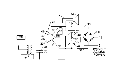
A typical audio frequency application of the
invention is depicted schematically in Fig. 2. Audio
2s speaker 54, replacing generalized load 10 from Fig. 1,
is driven by output 30 of amplifier 22 to series
connection point 43. As shown, the power amplifier
circuit 20 includes rectifier 56, which is preferably a
bridge rectifier, which rectifies current from AC line
3o source 58, which is typically a 120 VAC, 60 Hz or
similar common household line source. First bias level
36 and second bias level 38 are developed by rectifier
56 and typically include substantial ripple. For a 60
Hz, 120 VAC line current, the ripple on first bias
35 level 36 and second bias level 38 can be [2 V RMS], for
example. To DC isolate first amplifier input 23 and
second amplifier input 24 from input signal 50, which
is typically referenced to ground, the power amplifier
CA 02326102 2000-09-26
circuit 20 preferably includes input isolation means
such as balun 52 or other suitable audio frequency
transformer. To prevent high frequency oscillation of
amplifier 22 and resulting transistor damage in the
absence of any reference to ground, some trim
capacitance, such as 0.002 microFarads, is preferably
included between the base and the emitter of the first
transistor stage of amplifier 22.
In operation, power amplifier circuit 20 may
io be mounted in or on the enclosure for speaker 54.
Power amplifier circuit 20 typically includes an AC
power plug which is plugged into a wall socket
providing AC line source 58, and bridge rectifier 56
develops substantially constant first bias level 36 and
second bias level 38, charging first capacitor 40 and
second capacitor 42 and providing bias current to
amplifier 22 as shown in Figure 3. First capacitor 40
and second capacitor 42 are each preferably fairly
large capacitors, such as at least 1000 microFarad
ao capacitors, and may each comprise the parallel
connection of two or more capacitors. Audio-frequency
input signal 50 is DC isolated and ground isolated from
amplifier 22 via balun 52 and excites the differential
input to amplifier 22 defined by first amplifier input
2s 23 and second amplifier input 24. Amplifier 22, in
response to input signal 50, drives speaker 54 to DC-
isolated series connection point 43 between charged
first capacitor 40 and charged second capacitor 42.
Ripple present at series connection point 43 from
3o ripple developed by rectifier 56 on the voltage
potential across first bias level 36 and second bias
level 38 is compensated for to some extent by feedback
through third capacitor 44 connected between series
connection point 43 and second amplifier input 24.
3s The power amplifier circuit 20 and associated
method for amplifying a time-varying signal overcome
the size, weight and cost deficiencies of conventional
transformer-based audio amplifier power supplies by DCI
_8_
CA 02326102 2000-09-26
isolating the amplifier load, such as an audio speaker,
from the DC power source. Because the load is not
referenced to ground, the need for a power transformer
is eliminated and the size, weight and cost of the
s circuit may be reduced accordingly.
Many modifications and other embodiments of
the invention will come to mind to one skilled in the
art to which this invention pertains having the benefit
of the teachings presented in the foregoing descriptions
to and the associated drawings. Therefore, it is to be
understood that the invention is not to be limited to
the specific embodiments disclosed and that
modifications and other embodiments are intended to be
included within the scope of the appended claims.
i5 Although specific terms are employed herein, they are
used in a generic and descriptive sense only and not for
purposes of limitation.
-9-
CA 02326102 2000-09-26