Note: Descriptions are shown in the official language in which they were submitted.
CA 02326860 2000-11-24
1
SEMICONDUCTOR OPTICAL DEVICE
HAVING A COMPOUND SEMICONDUCTOR LAYER
INCLUDING ALUMINUM
BACKGROUND OF THE INVENTION
(a) Field of the Invention
The present invention relates to a semiconductor optical
device having a compound semiconductor layer including
aluminum (Al) and, more particularly, to a semiconductor optical
to device having a compound semiconductor layer having excellent
characteristics. The present invention also relates to a method
for selective growth of a compound semiconductor layer
including therein A1 in a semiconductor optical device.
m (b) Description of the Related Art
A semiconductor laser device known as an buried-ridge
semiconductor laser device includes ridge-shaped current
injection layers buried by current blocking layers at both sides of
the ridge. This type of semiconductor laser device is widely used
2o as a pick-up in the field of optical disk. An AIGaInP/GaAs
semiconductor laser device is a typical one among such buried-
ridge semiconductor laser devices, includes a GaAs current
blocking layer and emits light having a wavelength of 650 nm.
Fig. 1 shows a conventional buried-ridge AIGaInP/GaAs
2~ semiconductor laser device 10, which includes an n-type GaAs
CA 02326860 2000-11-24
2
(n-GaAs) substrate 12, and a layered structure formed thereon
and including a 1500-nm-thick n-AIGaInP ((AIZGaI-z)Xlnl-XP,
x=0.5 and z=0.7) lower cladding layer 14, GaInP/AIGaInP
multiple quantum well (MQW) layers 16, a 1500-nm-thick p-
AIGaInP ((AIZGaI-Z)Xlnl-XP, x=0.5 and z=0.7) upper cladding
layer 18, and a 300-nm-thick p-GaAs contact layer 20.
The top portion of the upper cladding layer 18 and the
contact layer 20 is configured as a ridge stripe, both sides of
which is buried by a GaAs layer 22 acting as a current blocking
layer. A p-side electrode formed on the contact layer 20 and an
n-side electrode formed on the bottom surface of the GaAs
substrate 12 are not depicted in the drawing.
A process for fabrication of the semiconductor laser device
10 of Fig. 1 is described with reference to Figs. 2A and 2B,
m which consecutively show fabrication steps of the semiconductor
laser device 10.
First, as shown in Fig. 2A, a 1500-nm-thick n-AIGaInP
lower cladding layer 14, GaInP/AIGaInP MQW layers 16, a
1500-nm-thick p-AIGaInP upper cladding layer 18 and an n-
2o GaAs contact layer 20 are consecutively grown on an n-GaAs
substrate 12 by a first epitaxial step using a MOCVD technique
to form a layered structure.
Subsequently, as shown in Fig. 2B, a SiN film is formed
on the contact layer 20, followed by patterning thereof to
25 configure a 5- ,u m-wide SiN stripe mask 24. The contact layer
CA 02326860 2000-11-24
3
20 and the top portion of upper cladding layer 18 are wet-
the
etched by using a sulfuric acid- or hydrochloric acid-based
etchant to form a ridge stripe 25.
Thereafter, a second epitaxial step is conducted to grow a
Si-doped n-GaAs current blocking layer 22 on both sides of the
ridge stripe 25 by a selective growth technique using the SiN
stripe mask 24 as a selective growth mask. Further, a p-side
electrode and an n-side electrode are formed on the contact layer
20 and the bottom surface of the GaAs substrate 12, respectively.
1o After cleavage of the wafer, a plurality of semiconductor laser
devices 10 such as shown in Fig. 1 are obtained.
In the conventional semiconductor laser device shown in
Fig. since the GaAs current blockinglayer 22 has a bandgap
1,
energy lower than the bandgap energy of the GaInP/AIGaInP
15 MQW layers 16, there is a problem in that the GaAs current
blocking layer 22 absorbs the light emitted by the MQW layers
16 and lowers the emission efficiency of the semiconductor laser
device.
It has been proposed for solving the above problem to
2o replace the material(GaAs) for the currentblocking layer 22
by
another material, such as Al(Ga)InP, which is optically
transparent to the lasing wavelength.
On the other hand, if a source gas including TMAI or
TMIn is used in the above selective growth step, wherein
25 Al(Ga)InP is deposited to form the current blocking layer
by
CA 02326860 2000-11-24
4
using the SiN selective growth mask, an undesirable
polycrystalline substance is deposited on the SiN mask because
the A1 atom in the source gas is formed as a nucleus of the
polycrystalline substance and the nucleus reacts with the other
components in the source gas to form the crystalline substance
around the nucleus.
The polycrystalline substance deposited on the SiN mask
has a strong bond with the SiN mask and is hardly etched by
hydrofluoric acid. Thus, although a wet etching for the SiN mask
to is conducted using hydrofluoric acid after the selective growth
process, the polycrystalline substance remains and the SiN
remains after the wet etching. This causes an uneven surface and
impedes the subsequent epitaxial steps. In addition, the
remaining polycrystalline substance and SiN mask adversely
15 affect the optical characteristics of the optical device as foreign
materials changing the composition of the compound
semiconductor layers. This problem is common to selective
growth processes using selective growth masks other than the
SiN mask in the semiconductor optical devices.
2o The deposition of the polycrystalline substance itself may
be prevented by a higher temperature or a lower growth rate in
the epitaxial growth of Al(Ga)InP, as employed in the
conventional technique.
However, a higher temperature degrades the laser
25 characteristics because Zn injected as doping impurities in the p-
CA 02326860 2000-11-24
AIGaInP upper cladding layer are diffused into the MQW layers.
On the other hand, a lower growth rate degrades the throughput
of the fabrication.
In the conventional fabrication technique for the
semiconductor laser devices, a variety of problems are also
encountered in the selective growth of compound semiconductor
materials including Al contents, such as AIGaAs and AIGaInAs,
other than the selective growth of the current blocking layer as
described above. This is caused by the fact that the Al content
therein forms a nucleus and is then reacted with other
components in the source gas during the selective growth step.
The selective growth technique as described heretofore is
also used for a selective area growth process. The selective area
growth process is such that a compound semiconductor is grown
to form a film on a specified growth area exposed by a pair of
growth prevention masks, for example, which are formed on the
area other than the specified growth area for prevention of
deposition of the compound semiconductor thereon. In this
technique, there is an advantage in that the thickness and the
2o contents of the resulting film can be controlled.
SUMMARY OF THE INVENTION
In view of the above, it is an object of the present
invention to provide a semiconductor optical device having a
compound semiconductor layer deposited by a selective growth
CA 02326860 2000-11-24
6
process and having excellent layer characteristics.
It is another object of the present invention to provide a
method for fabricating a semiconductor optical device, which is
capable of preventing deposition of a polycrystalline substance
during a selective growth of a compound semiconductor
including Al.
The present invention provides a semiconductor optical
device including a semiconductor substrate, and a layered
structure formed thereon, the layered structure including a first
1o conductivity-type current injection layer formed as a ridge stripe
and a second conductivity-type current blocking layer burying
the current injection layer at both side of the ridge stripe,
wherein the current blocking layer is doped with impurities
including at least carbon.
15 Examples of the semiconductor optical device according
to the present invention include a light emitting/receiving
semiconductor device, an optical waveguide, an optical amplifier
and an integrated semiconductor optical device including two or
more of them. The current blocking layer may be an AIGaInP
20 or AIGaAs layer in the case of a semiconductor optical device
formed on a GaAs substrate, or an AIGaInAs layer in the case of
a semiconductor optical device formed on an InP substrate. The
impurities for doping the current blocking layer may include at
least one of Si, Se and Zn in addition to carbon, whereby a
25 semiconductor optical device can be achieved which includes a
CA 02326860 2000-11-24
7
desired current blocking layer having an excellent controllability
with respect to the conductivity-type and the carrier density
thereof.
In accordance with the semiconductor optical device of he
present invention, the current blocking layer doped with
impurities including carbon affords a desired device
characteristic in the semiconductor optical device.
The present invention provides a method including the
steps of forming a compound semiconductor layer overlying a
to substrate and including Al, and forming a semiconductor optical
device including the compound semiconductor layer, wherein the
compound semiconductor layer forming step uses a mixture of
source gas for the compound semiconductor layer and halogen
compound gas including halogen and carbon.
15 The present invention provides, in one aspect thereof, a
first method including the steps of forming a current inj ection
layer overlying a semiconductor substrate and configured as a
ridge stripe,epitaxiallygrowing a currentblocking layer doped
with at leastcarbon and burying the ridgestripe at both sides
of
2o the ridge stripe by using a mixture of source gas for the current
blocking layer and additional halogen compound gas including
carbon atoms and halogen atoms, and forming a semiconductor
optical device including the current injection layer and the
current blocking layer.
In accordance with the first method of the present
CA 02326860 2000-11-24
8
invention, the epitaxial growth of the current blocking layer can
be conducted at a lower temperature with a high throughput.
The present invention also provides, in another aspect
thereof, a second method including the steps of selectively
s growing a compound semiconductor layer including A1 by using
a selective area growth mask while introducing a mixture of a
source gas for the compound semiconductor layer and additional
halogen compound gas including carbon atoms and halogen
atoms, and forming a semiconductor optical device including the
1o compound semiconductor layer.
In accordance with the second method of the present
invention, the mixture of source gas and additional halogen
compound gas suppresses deposition of polycrystalline
substance, and affords excellent controllability of the
15 conductivity-type and the carrier density of the compound
semiconductor layer.
The present invention also provides, in another aspect
thereof, a third method including the steps of selectively
growing a compound semiconductor layer including A1 by using
2o a selective growth mask while introducing a mixture of source
gas for the compound semiconductor layer and etching gas
including bromine, and forming a semiconductor optical device
including the compound semiconductor layer.
In accordance with the third method of the present
25 invention, the etching gas including bromine suppresses
CA 02326860 2000-11-24
9
deposition of polycrystalline substance to achieve a higher
selectivity in the selective growth process substantially without
involving an adverse effect in the resultant compound
semiconductor layer.
The above and other objects, features and advantages of
the present invention will be more apparent from the following
description, referring to the accompanying drawings.
BRIEF DESCRIPTION OF THE DRAWINGS
1o Fig. 1 is a sectional view of a conventional buried-ridge
semiconductor laser device.
Figs. 2A and 2B are sectional views of the semiconductor
laser device of Fig. 1, showing consecutive steps for fabrication
thereof.
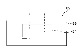
15 Fig. 3 is a top plan view of the semiconductor optical device
fabricated in the third experiments.
Figs. 4A and 4B are photographs taken by an optical
microscope for the comparative example and embodiment
obtained in the third experiments, respectively.
2o Fig. 5 is a graph showing the relationship between the
deposited particles and the flow rate of CBr4.
Figs. 6A to 6C are schematic perspective views of a
semiconductor laser device formed in the fourth experiments,
showing consecutive steps for fabrication thereof.
25 Fig. 7 is a sectional view of a semiconductor laser device
CA 02326860 2000-11-24
according to an embodiment of the present invention.
Fig. 8 is a graph showing relationship between the deposited
amount of polycrystalline substance and the flow rate of CBr4.
Fig. 9 is a graph showing relationship between the carrier
5 density and the flow rate of CBr4.
Fig. 10 is a graph between the threshold current and the
carrier density with the growth temperature being a parameter.
Fig. 11 is a top plan view of selective area growth masks on
a semiconductor substrate.
1o Figs. 12A and 12B are sectional views taken along lines A-
A' and B-B' in Fig. 11.
Figs. 13A and 13B are sectional views of deposited films
taken along lines A-A' and B-B' in Fig. 11.
Fig. 14 is a graph showing the thickness distribution of
selectively grown layer.
Fig. 15 is a graph showing the lasing wavelength emitted
from the areas shown in Fig. 11.
Figs. 16A to 16B are perspective views of a semiconductor
laser device according to an embodiment, showing consecutive
2o steps of fabrication thereof.
Figs. 17A and 17B are perspective views of a semiconductor
laser device, showing selective area growth.
Fig. 18A to 18F are perspective views of a semiconductor
laser device, showing butt joint growth.
CA 02326860 2000-11-24
11
PREFERRED EMBODIMENTS OF THE INVENTION
Now, the present invention is more specifically described
with reference to accompanying drawings, wherein similar
constituent elements are designated by similar reference
numerals throughout the drawings.
Before describing embodiments of the present invention,
the principle of the present invention is described with reference
to the experiments conducted by the present inventors.
The present inventors considered that the above problems
to could be solved by changing the contents of the source gas in the
selective growth of the Al(Ga)InP to form a current blocking
layer, and thus conducted a variety of experiments using
a
variety of source gases to selectively grow Al(Ga)InP current
blocking layers, as detailed below.
15 First Experiment
In these experiments, halogen compound gases each
including carbon and halogen, such as CBr4 and CC14, are used
as the source gases.
It was confirmed from the experiments that the halogen
2o atoms in the halogen compound gas had a function for etching
the polycrystalline substance deposited during the selective
growth, whereby even a lower-temperature selective growth
achieved suppression of the deposition of polycrystalline
substance.
25 In addition, it was also confirmed that the carbon atoms in
CA 02326860 2000-11-24
12
the halogen compound gas enters the Al(Ga)InP compound to be
doped in the resultant film, whereby the conductivity of the n-
type film can be controlled.
More specifically, the polycrystalline substance, which is
formed by reaction of A1 with the contents in the source gas, is
removed as a growth nucleus in the initial stage of the growth by
the etching function of CBr4 or CCl4, whereby generation of the
polycrystalline substance can be suppressed.
It was also confirmed in the experiments that C-doped
to Al(Ga)InAs could be grown as the current blocking layer in the
case where the ridge is buried by an AIInAs layer in an
AIGaInAs/InP-based semiconductor laser device formed on an
InP substrate.
It was also confirmed in the experiments that C-doped p-
AIGaAs could be grown as the current blocking layer in the case
where the ridge is buried by an AIGaAs layer in an
AIGaAs/GaAs-based semiconductor laser device formed on a p-
GaAs substrate.
2o As to the deposition problem of the polycrystalline
substance, it was also confirmed effective to use the epitaxial
growth technique using a mixture of source gas and halogen
compound gas including carbon and halogen, such as CBr4 or
CCl4, in the selective area growth process, as well as in the
2s burying growth process for deposition of the current blocking
CA 02326860 2000-11-24
13
layer as described above.
It is known in the selective area growth of a compound
semiconductor layer including Al, that the thickness of the
resultant compound semiconductor layer is significantly smaller
than the thickness of a typical current blocking layer. Although
the deposition of the polycrystalline substance may be
suppressed to some extent by employing a lower growth rate or a
lower ratio of group-V atoms to group-III atoms, a small amount
of the additional halogen compound gas including halogen and
to carbon suppresses the deposition of polycrystalline substance
more assuredly, and thus enables the concentration of carbon to
be reduced to a lower rate in the resultant layer thereby allowing
a more accurate control of the carrier density therein.
CBr4 gas, if used for deposition of a barrier layer in MQW
is layers as the additional halogen compound gas, allows a
modulated doping of the barrier layer. In this case, an effective
modulating doping can be achieved due to improvement of
selective growth characteristics and restricted diffusion of the
doped carbon.
2o As described before, although the conventional technique
used a lower growth rate or a higher growth temperature for the
suppression of polycrystalline substance, the suppression was
only limited. In addition, since these measures deviate from an
optimum growth rate, the device characteristics were degraded.
25 For example, the lower growth rate, if used for a compound
CA 02326860 2000-11-24
14
semiconductor including Al, increases the density of impurities,
such as oxygen, and thereby degrades the optical and electric
characteristics of the resultant layer.
It was also confirmed in the experiments based on the
methods of the present invention that an etching gas, if
introduced in the growth chamber, i.e., onto the substrate during
the selective growth of the compound semiconductor layer
including Al, the deposition of the polycrystalline substance
could be further suppressed.
to Among the experiments conducted, the following third and
fourth experiments will be described for a better understanding
of the present invention. In these experiments, an etching gas
including bromine was used instead of an etching gas including
chlorine because the latter is likely to damage the deposition
15 system and the natural environment.
Third ~xneriment
As an example of general selective growth processes,
AIInAs layer was grown on an InP substrate covered with a
mask pattern based on the principle of the present invention.
2o With reference to Fig. 3, in the present experiments, a 100-nm-
thick SiN film 64 was deposited on an InP substrate 62 by a
plasma-enhanced CVD technique, followed by photolithography
and wet-etching using hydrofluoric acid for patterning to obtain
a selective growth mask 64 having a width of 80 ,u m and a
25 length of 600 ,u m.
CA 02326860 2000-11-24
By using a source gas including trimethyl indium (TMIn),
trimethyl aluminum (TMAI) or arsine (AsH3) in each of the
experiments, a 500-nm-thick AIInAs layer 66 was formed on the
masked substrate, using a MOCVD technique, at a temperature
of 680°C, a pressure of 100 hPa and a growth rate of 1.8 ,u m.
As a comparative example, an AIInAs layer was formed
without supplying the etching gas in the growth chamber. In the
comparative example, as shown in Fig. 4A, polycrystalline
substance (appearing as dark spots) was deposited in a large
to amount, difficult to remove by later etching, and became an
impediment for the process in the subsequent steps. The
polycrystalline substance degraded the yield of the final products.
Fig. 4A, as well as Fig. 4B described below, is obtained by
using an optical microscope, wherein the dark area is formed by
15 the mask, and the white areas disposed at top and bottom
portions of the film were formed by the AIInAs layer.
As an example of the present experiments, carbon
tetrabromide (CBr4) gas was added to the source gas at a flow
rate of 3.2 ,u mol/minute in the growth chamber during the
2o selective growth of the AIInAs layer. The resultant layer is
shown in Fig. 4B, wherein the amount of polycrystalline
substance deposited on the mask was reduced to substantially
zero.
Quantitatively, the amount of polycrystalline substance
was reduced together with the increase of the flow rate of CBr4
CA 02326860 2000-11-24
16
gas, as shown in Fig. 5, wherein addition of no CBr4 gas caused
200 X 103 particles/mm2 of polycrystalline substance deposited
on the mask, addition of CBr4 gas at a flow rate of 1.6 ,~
mol/minute reduced the number of particles deposited on the
mask down to 100 X 103 particles/mm2, and addition of CBr4 gas
at a flow rate of 3.2 ,~ mol/minute reduced the number of the
particles to substantially zero, as shown in Fig. 4B.
Addition of CBr4 sometime changed the composition and
lowered the growth rate of the resultant layer, which was formed
0 on the growth area exposed from the selective growth mask
covering the non-growth area. It was confirmed that the change
of the composition and reduction of the growth rate could be
compensated by controlling the source gas, especially by
controlling the flow rates of group-III elements such as in the
~ compounds TMAI and TMIn.
It is preferable to experimentally determine the flow rate
of CBr4, which depends on the composition of the desired
AIInAs layer, especially the Al content thereof, the growth rate
and temperature thereof, and the size and surface roughness etc.
20 of the mask. The CBr4 gas can be replaced by other bromine gas
such as methyl bromide (CH3Br).
Fourth Experiment
These experiments were conducted for butt joint growth.
Figs. 6A to 6C show the process in these experiments. As shown
25 in Fig. 6A, a GaInAsP-based double-heterojunction (DH)
CA 02326860 2000-11-24
17
structure 74 including a GaInAsP MQW structure 73 was formed
on an InP substrate 72. Subsequently, a 100-nm-thick silicon
nitride (SiN) film was formed thereon, and subjected to
photolithography and wet-etching using hydrofluoric acid for
patterning to form a mask 76 having a width of 100 ,u m and a
length of 800 ,~ m. Thereafter, as shown in Fig. 6B, the DH
structure 74 and the underlying substrate were etched to a
specified thickness by using mask 76, thereby forming an
exposed surface 75 of the InP substrate 72.
to Subsequently, an AIGaInAs MQW structure 78 and an InP
layer 79 were consecutively formed by a selective growth
technique on the exposed surface of the InP substrate 72, as
shown in Fig. 6C. In the selective growth process, CBr4 was
supplied only during deposition of an Al-based compound
m semiconductor layer, or AIGaInAs layer in this example, at a
flow rate of 0.32 ,~ mol/minute. The flow rate of CBr4 depends
on the mask size. During the selective growth of AIGaInAs layer,
deposition of the polycrystalline substance was suppressed,
thereby achieving a high selective ratio.
2o It was then examined in the present experiments whether
or not the selective growth process using CBr4 caused adverse
affects against the crystalline structure or optical characteristics
of the resultant layer. The results were such that the crystalline
structure of the AIGaInAs layer, i.e., compound semiconductor
25 layer including Al, was not adversely affected by the selective
CA 02326860 2000-11-24
18
growth process with respect to the surface morphology and the
mirror surface thereof, and thus an excellent crystalline structure
was obtained.
With respect to the optical characteristics, the AIGaInAs-
s based MQW structure formed by the selective growth using CBr4
had photoluminescence characteristics and laser characteristics
similar to those in the AIGaInAs-based MQW structure formed
by the selective growth without using CBr4.
From the results of the third and fourth experiments as
to described above, it is confirmed that CBr4 gas supplied into the
growth chamber together with the source gas suppresses the
deposition of polycrystalline substance to improve the selectivity
in the selective growth process without involving degradation of
the crystalline quality of the resultant layer.
15 It is preferable to experimentally determine the flow rate
of bromine-based etching gas, which depends on a variety of
conditions including the composition of the compound
semiconductor layer including Al, especially the Al content
thereof, deposition conditions such as deposition temperature
2o and deposition rate, and the size or surface state of the mask
The compound semiconductor layer including Al and
formed by the selective growth process using the etching gas
including bromine atoms is not limited to have any specific
composition, and the examples of the compound semiconductor
25 layer include AIGaInP layer, AIGaAs layer, AIInAs layer, and
CA 02326860 2000-11-24
19
AIGaInAs layer. The composition of the etching gas including
bromine atoms is not limited to any specific composition, and
the etching gas may include CBr4.
The growth process using the etching gas including
bromine atoms may be a burying growth process, selective area
growth process or butt joint growth process.
Referring to Fig. 7, a semiconductor laser device,
generally designated by numeral 30, formed as an example of the
semiconductor optical device according to the present invention
to has a structure similar to that of the conventional semiconductor
laser device 10 shown in Fig. 1 except for the structure of the
current blocking layer 32.
More specifically, the semiconductor laser device 30
includes an n-GaAs substrate 12, and a layered structure formed
thereon and including a 1500-nm-thick n-AIGaInP ((AlZGa1_
Z)xlnl-xP, x=0.5 and Z=0.7) lower cladding layer 14,
GaInP/AIGaInP MQW layers 16, a 1500-nm-thick p-AIGaInP
((AIZGaI_Z)Xlnl_XP, x=0.5 and Z=0.7) upper cladding layer 18, and
a 300-nm-thick p-GaAs contact layer 20.
2o Among the layered structure, the contact layer 20 and the
top portion of the upper cladding layer 18 are configured as a
ridge stripe, both sides of which are buried by a C-doped n-
AIInP layer 32 acting as a current blocking layer. The C-doped
AIInP layer 32 has a carrier density of 1 X 1018 cm-3. The p-type
current injection area is isolated from the current blocking layer
CA 02326860 2000-11-24
32 by a p-n junction, whereby a current contraction structure is
achieved. A p-side electrode and an n-side electrode are formed
on the contact layer 20 and the bottom surface of the GaAs
substrate 12, respectively, although these electrodes are not
specifically shown in the figure.
The semiconductor laser device of Fig. 7 can be fabricated
as follows according to the first embodiment. The steps up to the
step of forming the ridge stripe 25 are similar to those described
1o with reference to Figs. 2A to 2B. The ridge stripe 25 is buried by
a C-doped n-AIInP current blocking layer 32 grown in a
selective growth step using a SiN selective growth mask, such as
the SiN stripe mask 24 shown in Figs. 2A.
The process conditions in the selective growth used for
15 forming a practical example of the AIInP current blocking layer
32 were as follows:
Growth temperature - 600°C ;
Flow Rate of Halogen compound gas CBr4 - S ,u mol/min.;
Flow Rate of Source gas for group-III TMAI and TMIn
20 (total) - 20 ,u mol/min.; and
Growth rate - 3 ,u m/hour.
The flow rate of CBr4 was determined based on the composition
which satisfies the matching condition with respect to the GaAs
substrate, taken in further consideration of etching effect of the
resultant layer.
CA 02326860 2000-11-24
21
The carrier density of the resultant C-doped AIInP layer
32 was 2 X 101' cm-3, which was somewhat lower compared to a
desired current blocking layer. Thus, the carrier density was
modified to assume 1 X 1018 cm-3 by adding SiH4 gas to
additionally dope the AIInP layer with Si.
The resultant AIInP current blocking layer 32 achieved a
carrier mobility which was comparable to the carrier mobility of
an ordinary Si-doped AIInP current blocking layer. That is,
electric characteristics were not degraded by the doping with
to carbon.
In the resultant structure, the 10- ,u m-wide mask was
substantially free from the deposition of polycrystalline
substance thereon after the selective growth of AIInP. Thus, it
was confirmed that the addition of CBr4 gas was effective for
suppressing the deposition of polycrystalline substance.
A variety of experiments were conducted with respect to
the addition of CBr4. Referring to Fig. 8, the amount of
polycrystalline substance deposited on the selective growth mask
is plotted in an arbitrary unit against the flow rate of CBr4 which
2o ranged zero to 8 ,~ mol/min. Fig. 8 was obtained by changing
the flow rate of CBr4 while maintaining the other conditions as
listed before.
The amount of deposited polycrystalline substance
generally depends on the growth conditions such as the growth
temperature, the flow rate of source gas for group-III element
CA 02326860 2000-11-24
22
and the Al content, and the configuration of the mask such as the
size thereof. In Fig. 8, a threshold for the amount of deposited
polycrystalline substance resides at a CBr4 flow rate of 5 ,u
mol/min, above which the deposition of polycrystalline
substance was substantially completely suppressed.
In the above experiments, if the ratio between the flow
rates of the source gas for group-III element and CBr4 gas is
below 2, the deposition rate of AIInP is substantially zero due to
the higher etching rate compared to the deposition rate thereof.
to On the other hand, if the ratio between the flow rates is above 4,
a sufficient suppression effect is not obtained for the deposition
of polycrystalline substance.
Thus, a preferable range of the ratio resides between 2 and
4 at a growth temperature of 600°C . If CBr4 is replaced by CC14,
the lower and upper limits of the range extend below 2 and
above 4, respectively, due to a higher etching function of CCl4
compared to CBr4.
If AIGaInP, which better lattice-matches with a GaAs
substrate, is selectively grown instead of AIInP, the lower limit
2o extends somewhat lower, whereas the upper limit of the range
extends significantly higher, due to a lower Al content in the
source gas for group-III elements.
Referring to Fig. 9, the carrier density in the AIInP layer,
which is selectively grown while being subj ected to doping with
2~ carbon, is plotted against the flow rate of CBr4. The carrier
CA 02326860 2000-11-24
23
density in the C-doped AIInP layer increases with the increase of
the flow rate of CBr4, and has a tendency of saturation in a
higher flow rate range of CBr4. The higher flow rate range may
also degrade the characteristics of the semiconductor optical
device. Accordingly, it may be preferable that another n-type
dopant, such as Se, be additionally used for achieving a desired
carrier density.
For suppression of the deposition of polycrystalline
substance on the selective growth mask, it may be correctly
o considered to lower the growth rate of AIInP layer itself.
However, the lower growth rate of AIInP layer lowers the
throughput of the semiconductor optical device and should not
be used, especially in the case of selective growth of the current
blocking layer which has a thickness of 1 !~ m or higher.
The selective growth of the AIInP layer according to the
present embodiment assures a relatively higher growth rate of 3
,~.~ m/hour and scarcely suffers from a lower throughput of the
growth.
The growth temperature as low as around 600 °C
2o suppresses the diffusion of Zn in the upper cladding layer. A
lower growth temperature is generally disadvantageous in view
of the higher deposition rate of polycrystalline substance.
However, the addition of CBr4 based on the present embodiment
cancels the disadvantage.
The suppression of Zn diffusion as described above allows
CA 02326860 2000-11-24
24
the Zn concentration of the upper cladding layer during the
initial epitaxial growth thereof to be higher, whereby the
threshold current of the semiconductor laser device can be
maintained at a lower value and the temperature characteristics
can be improved.
Referring to Fig. 10, the threshold current of the
semiconductor laser device is plotted against the carrier density
of the upper cladding layer, with the growth temperature of the
AIInP layer as a parameter.
to Solid line (1) is taken before the burying epitaxial growth
and after the initial growth of the layered structure, whereas
dotted line (2) and chain line (3) are taken after the burying
epitaxial growth. Dotted line (2) indicates the relationship at a
growth temperature of 700 °C in a conventional technique
is without addition of CBr4, and chain line (3) indicates the
relationship at a growth temperature of 600 °C in the
embodiment.
Dotted line (2) indicates that the threshold current in the
conventional technique abruptly increases above a carrier
2o density of approximately 1.5 X 1018 cm-3 due to the diffusion of
Zn caused by the heat generated during the burying growth. On
the other hand, chain line (3) indicates that the threshold current
in the embodiment using CBr4 gas stays at a lower level
comparable to the level of solid line (1) up to a carrier density of
25 3 X 1018 cm-3 due to a lower growth temperature of 600°C .
CA 02326860 2000-11-24
A semiconductor laser device including an AIGaInAs
current blocking layer was fabricated according to the second
embodiment of the present invention. Fig. 11 shows a top plan
5 view of a pair of selective area growth masks used therein, Figs.
12A and 12B are taken along lines A-A' and B-B', respectively,
in Fig. 11.
As shown in Figs. 11, 12A and 12B, a pair of SiN masks
44 were formed on an n-InP substrate 42, wherein each of the
to masks 44 had a width (W) of 50 ,u m and the gap (G) between
the masks 44 was 10 ,~ m. The surface area 46 of the substrate
42 between the masks 42 is exposed and called a mask gap area.
The area 45 of the substrate 42 is a normal growth area, which is
not substantially affected by the presence of the masks 42 due to
m a sufficient distance from the masks 42.
Subsequently, a 50-nm-thick n-InP lower cladding layer
48, a 100-nm-thick AIGaInAs layer ( ~l g=1000nm) light
confinement layer 50, MQW layers 52, a 100-nm-thick
AIGaInAs layer ( ~ g=1000nm) light confinement layer 54 and a
20 300-nm-thick p-InP layer 56 were consecutively grown on the
disposed surface of the substrate 42 by a MOCVD technique
using the SiN masks 44 as a selective area growth masks.
The n-InP lower cladding layer 48 was doped with Se to
have a carrier density of 1 X 1018 cm-3. The MQW layers 52 were
25 such that each of the well layers had a thickness of 5 nm and a
CA 02326860 2000-11-24
26
strain of +1.0%, each of the barrier layers had a thickness of 10
nm and a composition corresponding to ~ g=1000 nm, and the
number of well layers is six. The p-InP layer 56 was doped with
Zn to have a carrier density of 1 X 1018 cm-3.
The process conditions for the growth were such that the
growth temperature was 650°C, the growth rate at the normal
growth area 45 was set at 1.2 ,~ m/hour, and CBr4 gas was
introduced at a flow rate of 2 ,u mol/min. during growth of the
AIGaInAs layer in addition to the source gas for AIGaInAs.
to Figs. 13A and 13B show after the selective growth and
were taken along lines A-A' and B-B', respectively, in Fig. 11.
After the selective area growth, the film thickness of the mask
gap area 46 is higher by about twice than the film thickness of
the normal growth area 45, as shown by the profile shown in Fig.
15 14.
As a result of the difference in the deposition thickness,
the lasing wavelength of the MQW layers is longer in the mask
gap area 46 than in the normal growth area 45. This is shown in
Fig. 15, wherein the lasing wavelengths are 1300 nm and 1150
2o nm, respectively, in the mask gap area 46 and the normal growth
area 45.
By taking advantage of the principle of the above
embodiment, a new structure of a semiconductor optical device
can be formed wherein the mask gap area 46 is formed as a laser
25 element and the normal growth area 45 is formed as a waveguide
CA 02326860 2000-11-24
27
area for passing the laser emitted by the laser element
substantially without absorbing the laser. Both the laser element
area and the waveguide area can be formed by a common growth
process.
In the above embodiment, the flow rate of the CBr4
introduced during deposition of AIGaInAs layer which was as
low as 2 ~c mol/min. scarcely affected the electric
characteristics of the AIGaInAs layer due to a smaller carbon
dosage of the AIGaInAs. The addition of CBr4 gas suppressed
to the deposition of polycrystalline substance on the masks as
encountered in the conventional process.
The lower flow rate of CBr4 allows the AIGaInAs layer,
i.e., compound semiconductor layer including Al, to have either
the n-conductivity or the p-conductivity depending on doping the
15 layer with Se or Zn. Thus, electric characteristics of the layer
can be controlled as desired.
A modulation doping process for the barrier layers was
also conducted for trial by increasing the flow rate of CBr4
during growth of the barrier layers up to 20 ,~ mol/min., which
2o resulted in a carrier density of 1 X 1018 cm-3 in the barrier layer
due to the increased carbon doping. This modulation doping
function may be practically used for modulation of the barrier
layers in a MQW structure.
Third Embodiment or Fabrication
25 Referring to Figs. 16A to 16D, the principle of the present
CA 02326860 2000-11-24
28
embodiment is applied to a semiconductor laser device having a
ridge stripe (or mesa structure).
In Fig. 16A, an AIGaInP-based double heterojunction
structure 82 including GaInP/AIGaInP MQW layers 81 is formed
on an n-GaAs substrate 80. Subsequently, as shown in Fig. 16B,
a stripe mask 84 is formed on the DH structure 82, followed by
selective etching of the DH structure 82 by using the stripe mask
84 to configure a ridge stripe 86.
Thereafter, as shown in Fig. 16C, a p-AIInP layer 88 and
o an n-AIInP layer 89 are consecutively grown based on the
principle of the present embodiment as current blocking layers
for burying the ridge stripe 82 by the current blocking layers 88
and 89 at both sides thereof using the stripe mask 84 as a
selective growth mask. After growing a p-AIGaInP cladding
layer and p-GaAs contact layer on the entire area, a p-side
electrode and an n-side electrode are then formed on the top and
bottom, respectively, of the wafer, thereby achieving a
semiconductor laser device.
Referring to Figs. 17A and 17B, a selective area growth
2o technique will be described, wherein a pair selectivegrowth
of
masks 92 are types optical
used for fabricating of
different
elements on a single semiconductor substrate 90. The pair
of
selective growth masks 92 are formed on a first of the
area
substrate 90 with a small space therebetween, second
whereas a
area has no such mask, as shown in Fig. 17A. ing
By us the
CA 02326860 2000-11-24
29
selective area growth masks 92, DH structures 94 and 96 are
grown in the first and second areas, respectively, of the substrate
90 based on the principle of the present embodiment. The
principle of the present embodiment is used in growth of a
compound semiconductor layer including Al, e.g., an AIGaInP
layer. The DH structure 94 in the first area is of a ridge stripe
and has a larger height, whereas the DH structure 96 has a
uniform height.
In the second embodiment of fabrication for the AIGaInAs
to layer, light confinement layers are grown based on the principle
of the present embodiment.
A butt joint growth as mentioned before was used in the
fourth experiments, and is preferably applied to fabricating an
integrated optical device including a semiconductor laser device
and an optical modulator.
Figs. 18A to 18B show consecutive steps of the butt joint
growth process, wherein MQW slayers 101 and MQW layers 105
are grown by the butt joint growth process in the first and second
2o areas, respectively.
In Fig. 18A, after forming a diffraction grating, a DH
structure 102 including MQW layers 101 is grown on the entire
area of an InP substrate 100, to form a layered structure of a
distributed feedback laser device (DFB-LD). Subsequently, as
2~ shown in Fig. 18B, a SiN mask 104 is formed on the top of the
CA 02326860 2000-11-24
first area, followed by etching of the DH structure 102 exposed
from the SiN mask 104 as well as the top portion of the InP
substrate 100 in the second area. The portion of the DH structure
102 left in the first area is formed as a laser device.
Subsequently, as shown in Fig. 18C, a DH structure 106 of
an optical modulator including MQW layers 105 having a lasing
wavelength of 1500 nm is grown on the exposed surface of the
InP substrate 100 by using the selective growth technique based
on the present embodiment.
1o Thereafter, the SiN mask 104 is removed, and another
stripe mask 108 is formed on the top surface in the first and
second areas, as shown in Fig. 18D. Then, as shown in Fig. 18E,
DH structures 102 and 106 are etched together with the top
portion of the InP substrate 100 by using the SiN mask 108 as an
m etching mask, to form a mesa stripe extending in the first and
second areas and expose the InP substrate 100 at both sides
thereof. Subsequently, as shown in Fig. 18F, a Fe-doped InP
current blocking layer 110 is grown by a selective growth
technique using the SiN mask 108 as a selective growth mask to
2o bury the mesa stripe at both sides thereof. Thereafter, n-side and
p-side electrodes are formed in each of the first and second areas
to achieve a laser device and an optical modulator in the first
and second areas, respectively, whereby an integrated
semiconductor optical device can be obtained.
25 Since the above embodiments are described only for
CA 02326860 2000-11-24
31
examples, the present invention is not limited to the above
embodiments and various modifications or alterations can be
easily made therefrom by those skilled in the art without
departing from the scope of the present invention.