Note: Descriptions are shown in the official language in which they were submitted.
CA 02327428 2000-10-04
WO 99/53351 PCT/EP99/02421 -
1
METHOD FOR CONNECTING OPTICAL FIBER AND OPTICAL WAVEGUIDE
Background of the Invention
1. Field of the Inven,~on
The present invention generally relates to the field of high speed fiber
optical
communications, and more particularly to methods for joining optical fibers
with integrated
optical waveguides.
2. Technical Hackaround
~o It is typical to connect an optical fiber to an optical waveguide, for
instance, when
preparing an integrated optics device for use in a communications system or
network. The
term "optical waveguide" is used herein, in distinction to the expression
"optical fiber," to
designate a lightguiding medium typically formed on or in a planar (silica)
substrate of
rectangular cross-section (or a chip as referred to interchangeably herein).
Note that the
is term "planar waveguide" conventionally refers to a unit comprising a core
and a cladding
region; that is, a light path and the substrate in or on which the light path
resides; however,
in the present application a distinction will be made between the lightpath
("waveguide")
and the substrate (or chip) when appropriate to avoid confusion. Typically,
the light
guiding region (core) extends to the edge or extremity of the chip. Waveguides
of this type
20 are frequently encountered in integrated optics applications, for example,
as components of
CONFIRMATION COPY
CA 02327428 2000-10-04
WO 99/53351 PCT/EP99/02421
2
a multiplexer or demultiplexer or, more generally, as part of an integrated
optical circuit.
The conventional fusion technique for connecting optical fibers together makes
use
of an electric arc discharge. However, this technique is not suitable for
connecting an
optical fiber to a waveguide due to the gcotnetrical characteristics of the
waveguide and the
heat capacity of the waveguide which is higher than that of the optical fiber.
Accordingly,
it has been proposed to connect an optical fiber to a planar type silica
waveguide by
bringing the elements into abutment and applying a laser beam to cause them to
fuse
together. However, a further problem arises: namely, a high energy laser beam
used to
create the fusion joint can cause the waveguide core to bend and, moreover,
excessive
to melting of the optical fiber can occur. On the other hand, if a lower
energy laser beans is
utilized, then the joint between the waveguide and the optical fiber has loss
xtrengch than
required for deployed applications.
One proposed approach to solving the above problem is to pre-heat the
waveguide
by means other than the laser beam used for effecting the fusion between the
waveguide
t5 and the optical fiber. Such pre-heating makes it possible to reduce the
power of the laser
beam needed to create the fusion connection. However, such an approach
complicates the
process for forming the fusion joint and, in many cases, requires the use of
specialised
equipment and/or the modification of the structure of the integrated optical
component to
be connected to the optical fiber.
2o Another consideration is the ever increasing demands being placed on
optical
communications technology which have complicated the hardware and software
involved,
and placed great emphasis on achieving more efficient manufacturing and
deployment. For
example, the growth of metm networks and the associated signal routiag,
add/drop and
switching requirement. for narrowband WDM systems employing 16, 32, or 40 or
more
25 channels now makes it advantageous to be able to connect multiple fibers to
respective
waveguides (referred to hereinafter as "mufti-fiber fusion pigtailing") with
good
performance characteristics, accuracy, repeatability, and efficiency rather
than single
fibcr/waveguide connections.
CA 02327428 2000-10-04
WO 99/53351 PCT/EP99/02421
3
The prexnt invention provides a method for forming an accurate fusion joint
between an optical fiber and an optical waveguidc in a chip, with low optical
losses and a
strong joint.
The invention further provides a method for accurately performing multi-fiber
fusion pigtailing between multiple fibers and multiple waveguides in a chip,
with low
optical losses and strong joints.
Summary of the Invention
An embodiment of the present invention provides a method for connecting an
optical feber to an optical waveguide in a chip, including the steps of
aligning the optical
fiber with the waveguide, bringing the optical fiber and waveguide into
abutment, and
irradiating a zone of abutment between the optical fiber and the wavcguide
with a laxr
beam having a sufficient power and a desired spatial energy distribution; and
blocking a
portion of the laser beam such that the energy cowespoading to a substantially
central part
t5 of the spatial energy distribution is reduced with respect to the energy
corresponding to a
peripheral part of the spatial energy distribution in the beam at the zone of
abutment.
An aspect of this embodiment of the invention involves interposing a shield
element in the path of the laser beam upstream of the zone of abutment in
order to
eliminate a substantially contra! part of the laser beach while allowing a
peripheral part
thereof to pass.
According to another aspect of the invention, the step of reducing the energy
in the
substantially central part of the spatial energy distribution with respect to
the peripheral
part is carried out by dividing the laser beam, upstream of the zone of
abutment, into
several distinct beams, and directing thex beams towards the zone of abutment.
This can
be done, for example, by a splitting mirror disposed in the path of the laser
beam upstream
of the zone of abutment, with the distinct beams then directed towards the
zone of
abutment by pat~bolic mirrors. The distinct beams resulting from the splitting
of the laser
beam can b~~ slightly defocused at the zone of abutment.
CA 02327428 2000-10-04
WO 99/53351 PCT/EP99/024Z1
4
Another aspect of the invention relates to accurately positioning the none of
abutment with respect to the location of a focused or slightly defocused laser
beam for
fusing the waveguide to the optical fiber. This method aspect involves the
steps of
obtaining an image of the laser beam on the waveguidc chip surface and
generating a set of
coordinates x,, y,, corresponding to the position of the approximate center of
the laser
beam. The coordinates x, and y, are set off from a border or extremity of the
chip by
respective amounts fix, Ay. A second set of coordinates, x= and y2, which
represent the
extremity position of the waveguide, arc then determined and the waveguide
extremity and
abutted fiber are manually or automatically located at a position ~X = x2- x,,
~Y = y~- y,;
that is, the zone of abutment is optimally and accurately positioned in the
fusion region of
the laser beam. The image of the lose: beam on the chip is obtained by a
camera which is
stationary, aloag with the laser, relative to the chip and the fiber.
Preferably, several
images are taken in sequential time order. The positioning method according to
the
invention provides a positioning accuracy of the zone of abutment of greater
than about
plus or minus one micron.
In another embodiment of the invention, a method for connecting a plurality of
optical fibers to a respective plurality of waveguides in a chip includes the
steps of
propagating a substantially collimated laser beam through a diffractive
optical clement
(DOE) to simultaneously produce a desired spatial laser energy distribution at
a Zone of
abutment for each of the fiber-waveguide connections.
An aspect of this embodiment provides a method for accurately positioning the
energy distributions of the laser beams at each zone of abutment and includes
the
positioning steps referred to in the positioning aspect described above.
The invention described herein provides a method for strongly, accurately, and
efficiently connecting an optical fiber to a waveguide in an optical chip.
In each of the aspects of this embodiment, the energy distribution at the zone
of
abutment is asymmetrical; that is, the energy impinging upon the waveguide is
greater than
that which reaches the optical fiber. In this way, the degree of melting of
the optical fiber
can be controlled.
CA 02327428 2000-10-04
WO 99/53351 PCT/EP99/02421
In another aspect of the embodiment of the invention, :~ forcx is applied
between the
optical fiber and the waveguide in a direction moving the optical fiber and
waveguide
closer together during the irradiation of the zone of abutment.
rn a further aspect, the power cycle of the laser is controlled such that the
laser
5 lxam power is held at a first, relatively higher level during a first period
of time during
which the fusion joint is created, and is maintained at a lower level during a
scxond period
of dmc subsequent to the first period of time, allowing gradual cooling of the
fusion joint.
The methods of the present invention find application in connecting optical
fibers to
planar silica waveguides. In orckr to ensure absorption of the laser energy by
the
to waveguide material, the irradiation step is performed using a laser beam of
wavelength
greater than 4~tm. Suitable lasers include a CO laser having a wavelength of
9.81rm, and a
C02 laser having a wavelength of 10.6pm. Use of a COz laser currently provides
a cost
advantage.
Additional features and advantages of the invention will be set forth in the
detailed
t5 description which follows, and in part will be readily apparent to those
skilled in the art
from the description or recognised by practicing the invention as described in
the written
description and claims hereof, as well a,S the appended drawings.
It is to be understood that both the foregoing general description and the
following detailed description are merely exemplary of the invention, and am
2o intended to provide an overview or framework to understanding the nature
and
character of the invention as it is claimed.
The accompanying drawings are included to provide a further understanding of
the
invention, and arc incorporated in and constitute a part of this
specification. The drawings
illustrate embodiments of the invention, sad together with the description
serve to explain
23 the principles and operation of the invention.
Brief Description of the Drawings
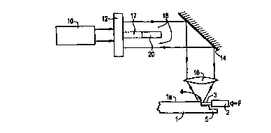
Figure 1 is a diagram illustrating the general disposition of the apparatus
used to put
into practice an embodiment of the invention;
CA 02327428 2000-10-04
WO 99153351 PCT/EP99/02421
6
Figure 2 is a diagram schematically illustrating the offset of the laser beam
with
respect to the boundary between the optical fiber and the waveguidc according
to an
embodiment of the invention;
Figure 3 is a graph illustrating a typical operating cycle of the laser
according to an
embodiment of the invention;
Figure 4 is diagram showing a further joint between the optical fiber and the
waveguide according to an embodiment of the ipvention;
Figure 5 is a diagram showing an apparatus for carrying out another embodiment
of
the invention:
to Figures 6A, 6B and 6C show laser beam energy distribution profiles;
Figure 7 is a diagram showing a particular arrangement of two laser beams
produced by the apparatus of Figure 5:
Figure 8 is a diagram !cchemadcally illustrating laser spot position control
according
to an embodiment of the invention;
~5 Figure 9 is a diagram schematically illustrating laser spot position
control according
to an embodiment of the irwention;
Figure 10 is a diagram schematically illustrating the waveguide extremity and
fiber
joint according to an embodiment of the invention;
Figure 11 is a diagram schematically illustrating mufti-fiber fusion
pigtailing
Zo according to an embodiment of the invention;
Figures 12A, 12B, 12C and 12D arc diagrams schematically illustrating laser
spot
geometries at the zone of abutment according to an embodiment of the
invention;
Figure 13 is a diagram schematically illustrating an optical set-up for mufti-
fiber
fusion pigtailing according to an embodiment of the invention;
2s Figure 14 is diagram showing an alternative stepped chip design for
providing a
robust connection with a fiber;
Figure 15 is a diagram schematically illustrating mufti-fiber fusion
pigtailing
according to another embodiment of the invention; and
CA 02327428 2000-10-04
WO 99/53351 PGT/EP99/02421
7
Figure 16 is a diagram schematically illustrating an optical set-up for mufti-
fiber
fusion pigtailing in accordance with Figure 15.
Detailed Description of Preferred Embodiments
Reference will now be made in detail to the present preferred embvdimeats of
the
invention, examples of which are illustrated in the accompanying drawings.
Wherever
possible, the same reference numbers will be used throughout the drawings to
refer to the
same or like pacts.
An exemplary embodiment of the method for connecting an optical fiber to an
optical waveguide formed in a chip according to the present invention can be
put into
practice using the method described herein in conjunction with the apparatus
illustrated in
Figure 1. This apparatus and method are used to form a fusion joint between a
silica
waveguide 1 a provided on a silica substrate 1 (constituting an integrated
optics chip) and
the end 3 of an optical fiber 2 aligned with the waveguide la. The end 3 of
the optical
is fiber 2 is stripped, i.e. the sheath protecting the latter is removed to
expose the silica pact
of the fiber. The end of the chip 1 preferably has a supped portion 5 to
accommodate the
stripped end 3 and the non-stripped portion of the optical fiber 2. A COZ
later 10 generates
a laser beam which is expanded and collimated by a component 12, reflected by
a mirror
14 and focused by a lens (or lens system) 16. The laser lxam is focused
substantially onto
2v the interface 4 between the optics! fiber and the waveguide, hereinafter
referred to
interchangeably as the zone of abutment or interface. The energy furnished by
the laser
beam to the zone of abutment 4 between the waveguide la and the stripped end 3
of the
optical fiber 2 presents a spatial distribution in which the energy
corresponding to a
substantially central part thereof is reduced with respect to that
corresponding to a
2s peripheral part, as illustrated in Figure 6C. The term "substantially
central part" is
understood to mean a central zone or one slightly offset relatively to the
center of the
energy distribution of the beam.
To achieve such a spatial energy distribution a beam blocking or shield
element 20
of preferably substantially cylindrical shape is disposed in the path of the
laser beam
CA 02327428 2000-10-04
WO 99/53351 1'CT/EP99/02421
8
advantageously after enlargement and collimation by component 12 but before
focusing by
element 16. In this way, the energy density falling upon the shield element 20
is lower than
in the case where the shield element were to be positioned before the
magnification unit or
after the focusing lens 16. This placement reduces local heating effects in
the shield
member 20. Moreover, by locating the shield element 20 at a poitrt in the
optical path of
the laser beam where the diameter thereof is relatively great, there is
increased accuracy in
the centering of the shield element ZO with respect to the laser beam. In
Figure 1 the shield
element 20 is located between the magnification unit 12 and the mirror 14 but,
in another
aspect, it could be located betw~n the mirror 14 and lens 16. The shield
element 20
to prevents a substantially central part 17 of the laser beam emitted by the
laser 10 to reach
the interface 4. The shield element 20 eliminates the energy corresponding to
this
substantially central part 17, while letting the remaining peripheral part 18
of the beam
propagate towards the interface 4. Taking into account the Gaussian
distribution of the
energy through the cross-section of the laser beam. the shielding or blocking
of the central
part 17 of the laser beam makes it possible to eliminate a high proportion of
the energy in
the central portion of the beam. Preferably, the diameter and the position of
the shield
element 20 arc selected such that 20 to 80°k of the energy of the beam
emitted by the lacer
10, and more preferably about 50% of the energy, is prevented from reaching
the elements
intended to be fused at the interface 4. The shield clement 20 should have
good thermal
zo conductivity so chat it can dissipate the significant energy produced by
the laser beam.
Prcferabiy, the length of the shield element 20 is selected to be as grant as
is practically
possible, in view of the desired size of the whole device, in order to
optimise energy
dissipation therein. In an exemplary aspect, the diameter and the length of
the element 20
are.5mm and lOmm, respectively. 1n addition, the material of the shield
element has a low
deformation when it is heated in order to ensure that the quantity of energy
eliminated from
the laser beam and the spatial distribution of the remaining energy are stable
and
reproducible. Steel and carbon are suitable exemplary materials for element
20.
The chip 1 incorporating the waveguide 1 a, and the optical fiber 2, are
mounted on
respective micro-positioning stages (not shown), positioned to abut against
one another and
CA 02327428 2000-10-04
WO 99/53351 PCT/EP99/02421
9
aligned in a conventional manner (typically by a conventional method which
maximises
light transmitted between the optical fiber and the waveguidc) as illustrated
in Figure 2.
With the optical fiber end 3 and chip l/waveguide la in abutment at the
interface 4, the
chip and fiber are positioned with respect to the laser beam as described in
greater detail
below. The COZ laser 10 is activated so as to generate, at a first, higher
power level, a laser
beam having a beam diameter of about 3.Smm which is expanded by the
magnifying/collimacing component 12 to a diameter of about l4mm, reflected by
the
mirror 14 and focused by the lens (or the lens system) 16 substantially on the
interface, or
zone of abutment, 4 between the optics! fiber 3 and the waveguide 1 a. The
diameter of the
lU laser beam after focusing by the element 16 is typically of the order of
150-400pm. The
laser beam is preferably slightly defocused at the zone of abutment 4, in
order to render the
spot produced by the beam slightly blurred at this zone.
Due to the presence of the shield element 20 in the optical path of the laser
beam,
approximately SO°~o of the beam energy produced by the laser 10 is
prevented from
is propagating towards the elements to be fu.~ed. Thus a relatively high power
laser beam can
be used in the process without causing bending of the waveguide core.
Preferably, the spot produced by the laser beam at the zone of abutment 4 is
not strictly
centered on the boundary of the optical fiber 2 and the wa~eguide 1 a, but
instead is offset
in the direction towards the waveguide by a distance ex. This offset ensures
that a greater
2o fraction of the beam energy reaches the waveguidc 1 a than the optical
fiber 2 which, due to
its specific heat capacity being lower than that of the waveguide, would tend
to melt to an
undesirable degree. In a typical case such as where the diameter of the laser
beam at the
interface is around 350~tm, the offset ~x should be between about 20-601rm.
Such a value
of the offset ensures that the desired temperature distribution is effected.
In particular, it is
25 thus possible to take the waveguide and the optical fiber to the same
temperature.
Furthcnnore, the laser beam is set at a first power level which is relatively
high in
order to cause local melting of the waveguide la and optical fiber end 3 at
the boundary 4,
as shown in Figure 3. A force, F, is applied so as to exert a gentle pressure
urging the
optical fiber towards the waveguidc. Alternatively, the force F may be applied
on the
CA 02327428 2000-10-04
WO 99/53351 PCT/EP99/02421
waveguide, or complementary forces may be applied on the wavcguide and optical
f ber 2.
In the absence of the application of a relative force between the waveguide
and the optical
fiber urging them towards each other, it has been found that the end 3 of the
optical fiber 2
deforms upon melting so as to create an empty space betw~n the optical fiber
and the
s waveguidc. Thus application of the force F is desirable in order to produce
a stroag fusion
joint with low optical losses. Typically. the application of force F causes a
relative
displacement between the optical fiber 2 and the waveguide la during the
fusion process,
this relative displacement being able to go up to about SOEun. As a result of
this relative
displacemeac, the end 3 of the optical fiber 2 may penetrate slightly into the
material of the
to waveguide. This further reinforces the strength of the fusion joint. After
the fusion of the
waveguide la and optical fiber 2, the power of the laser began is reduced to a
lower level
and, preferably, this power level is gradually reduced still further during a
relatively long
period of time in order to allow the fusion joint to cool down gradually. In
this way,
stresses in the fusion joint are reduced. Figure 3 illustrates a typical power
cycle of the C02
is laser during a cycle of the method according to the present invention.
Figure 3 also
indicates the time period during which the application of force F causes
movement of the
fiber 2 towards the waveguidc la, and the level of an optical signal
transmitted between floe
fiber 2 and waveguide 1 a for purposes of monitoring the progression of the
connection
process. It can be seen that the various steps of the connection cycle are
very short.
2o Therefore it is preferred that the displacements of the micro-positioning
stages, and the
power cycle of the laser, be computer-controlled. Typically, the power cycle
of the laser is
controlled by controlling the excitation current thereof using a control
signal.
Conventionally, the level of this control signal can in rum be fixed by
varying a regulation
current or voltage, depending upon the detailed implementation of the control
unit, all of
25 which is understood by those skilled in the art.
In an aspect of the invention, and in order to have a final device that is
mbust, it is
prefernd to supplement the fusion joint with a further polymer or mineral
joint 25, as
illustrated in Figure 4. The combination of this supplementary joint with the
stepped
portion 5 of the end of chip 1 ensures a particularly strong supplementary
bond between the
CA 02327428 2000-10-04
WO 99/53351 PCT/EP99/02421
11
optical fiber and the waveguide. Alternatively, as shown in Figure 14, a
monolithic chip 1
incorporating waveguide 1 a and having stepped portions 152, for connecting
with a fiber
(not shown) will also provide a robust device.
In the above discussion of the preferred embodiment, an asymmetric temperature
distribution is established across the boundary between the waveguidc and the
optical fiber
by offsetting the spot produced by the laser beam from the boundary. However,
other
means may be adopted for achieving this asymmetrical temperature distribution.
For
example, the desired distribution can be achieved by using a shield element 20
whoa cross
sectional shape (perpendicularly to the laser beam 17, 18) is such that the
laser beam
comprises more energy at positions which will be focused onto the waveguide
and
relatively less energy at positions which will be focused onto the optical
fiber 2. Such a
shielding clement 20 could, for example, be pear-shaped in cross section.
Alternatively,
the desired temperature distribution could be obtained by a combination of an
offset of the
laser beam and the use of a specially-shaped shielding element 20. Shielding
elements
IS other than those described hereinabove may also be used for eliminating
part of the energy
of the laser beam. For example, instead of using a cylinder, another element
of circular
cross-section, such as a cone, may be employed. Alternatively, elements not
presenting a
circular cross-section may be used: for example, elements whose section is in
the form of a
star, ellipsis, etc. Theoretically, a similar result is possible by using a
shield of circular
2o shape (or of different shape). substantially in two dimensions, or a thin
shielding element
xuch as a disc.
Furthermore, a laser other than a C4~ laser may be used as long as the
material of
the waveguide is capable of absorbing energy at the wavelength of the laser.
In the case of
a silica waveguide, this condition implies in practice chat the wavelength of
the laser is
25 greater than about 4pm.
In a preferred aspect of the embodiment described above, a method for
accurately
positioning the laser beam at the zone of abutment is described with reference
to Figures 8-
10. Refeaing first to Figures 8 and 9, a camera 108 that is fixed in position
relative to the
chip 1 and the fiber end 3 to be fused together provides an image in a field
of view 110
CA 02327428 2000-10-04
WO 99/53351 PCT/EP99/02421
12
surrounding and including the zone of abutment 4 between the waveguide and the
optical
fiber. A low power laser beam 18 from the COx laser is focused on the chap
within the
f:eld of view and image recognition software such as, e.g., Optimal'"' by
Imasys, is utilized
to generate a sot of coordinates x,, y, corresponding to the position of
substantially the
center of the focused laser beam. The location of the beans denoted by x~, y,
is sa off from
a border (or extremity) 112 of the chip 1 and the waveguide 2 by an amount
fix, Dy. The
extremity I 12 of the wavcguide is also identified and denoted by a set of
coordinates x2, yZ.
A quantity aX = x2 - x ~ and 0Y = y - y are calculated and the zone of
abutment 4 defined
as the waveguide exrlemity/fibcr interface are positioned at this coordinate
location. With
respect to an X-axis that is parallel to the waveguide in the chip, do is
preferably about
300~1m. For a chip having a waveguide pitch of about 350Erm, ~y is preferably
about
1751un along a Y-axis normal to the X-axix as shown in the coordinate system
accompanying Figure 9. It will be appreciated, however, that t1y will be
motivated by the
wavcguide pitch in all cases.
In an exemplary embodiment, a first image was obtained over a time of about 2-
3
seconds, and four subsequent images were obtained at 'approximately 0.4
seconds after
each preceding image. This method allowed the extremity of the waveguide to be
positioned to within about ~ lltm with respect to the approximate laser beam
center at the
zone of abutment. Figure 10 shows a marker identifying the extremity 112 of
the
2o waveguide 1 and the optical fiber end 3.
In an alternative preferred aspect of the invention as shown in Figure 5,
several
la.~er beams are generated to simultaneously irradiate the zone of abutment.
According to
this embodiment, a laser beam 40 produced by a laser source (not shown) is
directed
towards a splitting mirror 50 which splits the beam 40 into two distinct laser
beams 41 and
42. Each beam 41, 42 is then reflected by a respxtive parabolic mirror 60, 70
and focused
by this parabolic mirror on the interface 4 between the optical fiber 2 and
the waveguide
la. The splitting mirror 50 is preferably in the form of a triangular prism,
of which a
median line of the triangular emss-section (in the plane of Figure 5)
substantially merges
with the axis 43 of the laser beam 40, and of which two adjacent side faces
51, 52 disposed
CA 02327428 2000-10-04
WO 99153351 PC'T/EP99/02421
13
one either side of the axis 43 are reflecting. The laser beams 41 and 42
reflected
respectively by the faces S 1, 52 of the splitting mirror 50 are preferably
focused by the
parabolic mirrors on the zone of abutment 4 between the optical fiber end 3
and the
waveguide 1 a so as to be superposed thereon. Figure 6 illustrates the
modification of the
distribution of energy of the laser beam 40 by the optical elements 50, 60 and
70 during
irradiation of the zone of abutment between the optical fiber 2 and the
waveguidc la. The
Gaussian profile (cf. Figure 6A) of the energy distribution of the laser beam
40, in a plane
perpendicular to that of Figure 5, before splitting of the beam by the
splitting mirror 50, is
transformed at the zone of abutment into a substantially rectangular energy
profile, shown
in bmkcn lines in Figure 6B. This substantially rectangular profile
corresponds to the sum
of two Gaussian half curves respectively associated with the two beams 41, 42.
The profile of the energy distribution at the zone of abutment 4 between the
optical
fiber 2 and the waveguide 1 a as shown in Figure 6B therefore presents a
central part of
which the level of energy has been reduced to become of the same order as that
of the
is remaining peripheral part. In this way, the prexnce of a maximum of energy
at the center
of this distribution is avoided. However, it should be noted that the profile
of distribution
of energy at the zone of abutment is not necessarily rectangular. Figure 6C
shows another
example of distribution of energy in which the energy corresponding to a
substantially
central zone 80 of the energy distribution has been reduced with respect to
the remaining
2o peripheral part, i.e. the edges, 81 thereof. In the exemplary profile of
Figure 6C, the energy
at the edges 81 is greater than that at center 80. Such a profile is obtained
in this
embodiment by applying the two laser beams 41, 42 to two different spots at
the zone of
abutment 4, ac shown in Figure 7. The distribution profile shown in Figure 6C
is
substantially the same as that obtained in the first embodiment with the aid
of the shielding
25 element 20. Zn practice, the effect produced in the zone of abutment 4 by
the energy
distributions of Figures 6B and 6C is not very different since, in the cast of
a distribution
of the type of Figure 6C, the temperature distribution in the zone of abutment
between the
optical fiber 2 and the waveguide 1 a is substantially homogeneous due to the
thermal
diffusion which is produced in this zone of abutmtnt.
CA 02327428 2000-10-04
WO 99/53351 PCT/EP99/02421
14
According to an aspect of this embodiment, the laser beams 41, 42 irradiating
the
zone of abutment 4 between the optical fiber 2 and the waveguide la are
slightly defocused
at this zone of abutment, in order to render the spot produced by the beams 4
t , 42 slightly
blurred at the zone 4. In this way it is possible to spread the energy
distribution so as to
render the latter more homogeneous. Likewise the beams 41, 42 are preferably
applied on
the zone of abutment 4 so that the quantity of energy reaching the waveguide 1
a is greater
than that reaching chc optical fiber 2. To that end, the beams 41, 42 are
directed towards
the zone of abutment 4 so that the spot produced thereby at Zone 4 is offset
with respect to
the boundary between the wavcguide 1 a and the optical fiber 2, in a direction
towards the
to waveguide.
Another preferred embodiment of the invention describes a method for
connecting a
plurality of optical fibers to a respective plurality of waveguides in a chip,
that is, multi-
tiber fusion pigtailing, and is described blow with reference to FigurES 11-
13.
Referring first to Figure 11, a silica chip 1 incorporating a number of
waveguides la
to be connected at an extremity 112 of the chip to a respective number of
stripped ends 3 of
optical fibers 2 is illustrated. A respective number of laser beams 120 are
shown irradiating
the zones of abutment 4 between the waveguides and the fibers. In order to
produce the
aeries of laser beams and their associated intensity profiles as shown in
Figure 11, a
diffractive optical element (DOE) 130 as shown in Figure 13 is inserted in the
path of the
2o expanded and collimated laser beam. Depending upon the design of the DOE
130,
essentially any desired wavefront or series of wavefronts can be generated
resulting in a
preferred intensity distribution of the beam at the zones of abutment 4.
Figures 12A, I2B,
12C and 12D illustrate four different possible beam distributions produced by
the .DOE 130
including a uniform rectangular distribution 12A; a rectangular distribution
having a quasi-
Gaussian profile wherein the intensity between the tails and the central
portion of the
profile varies between about 1 to 10% 12B; a series of square distributions
12C; and ~a
series of circular distributions 12D, the latter two of which have a
periodicity or pitch
corresponding to that of the fiber/waveguides. The profile represented by 12B
is preferred
with respect to that of 12A for irradiating chips having a relatively smaller
width because
CA 02327428 2000-10-04
WO 99/53351 PCT/EP99/02421
of the greater influence of the chip border in a smaller chip on the heat
diffusion from the
laser beam. Chips of relatively greater width have a less significant
influence on the heat
diffusion arising from chip border considerations making the profile of 12A
more
advantageous for use with larger chips. Based upon the manufacturing
parameters of the
5 DOE 130, optimized wavefronts can be generated which meet the fusion
temperature
requirements and the spatial energy distributions at the zones of abutment to
fuse the joints
while not adversely melting the fiber or warping the substrate as identified
above as
problems associated with conventional laser fusion methods.
As shown in Figure 13, a COx laser 10 generates a beam that is expanded and
t o collimated by component 12. In a preferred embodiment of the invention,
the collimated
beam is propagated to a reflecting element 140 and then through a DOE 130
which
products a desired intensity distribution at the zones of abutment 4 for multi-
fiber fusion
pigt.siling a series of optical fibers 2 and waveguides la in a silica chip 1.
The DOE 130
provides the additional function of focusing the beam at the zones of abutment
or at least
t5 providing a slightly defocused beam as may be stutable for attaining the
desired energy
distribution at the zones of abutment. However, depending upon DOE cost and
design
considerations, the focusing function may be performed by an additional
appropriate lens
element, such as a ZnSe lens (not shown) positioned upstream of the DOE.
In the case of multiple cncrgy distributions irradiating a respective
.plurality of
2o zones of abutment at the chip interface, it is preferred to accurately
position the beam
similarly to the single fusion case described above. According to an aspect of
the current
embodiment, and with reference to Figures 8 and 9, a low power intensity
distribution from
the laser irradiates the chip within a field of view of a camera in order to
obtain an image of
the laser beam on the chip. In the case of multiple intensity distributions
such as in Fgure
12C and 12D, it is only necessary to obtain an image of a single intensity
profile as the
periodicity and shape of the totality of profiles are fixed by the design of
the DOE as
described above. Thus it is possible to obtain from the image obtained via
image
acquisition software as described herein above, a coordinate x, corresponding
to the
position of substantially a center of the beam along an X-axis parallel to the
waveguide in
CA 02327428 2000-10-04
WO 99/53351 PCT/EP99/02421
16
the chip, wherein x, is set off from a border of the chip and the waveguide,
respectively, by
an amount a,x. The extremity of the wavcguide along the X-axis is assigned the
coordinate
x2. The waveguidc extremity and the optical fiber, which are abutted as
described above,
are then positioned at a location defined by AX = x2 - x,. Positioning of the
beam
s according to the method described herein provides a positioning accuracy of
~l~tm or
better. Such positioning accuracy assures a good reproducibility of the heated
area of the
zone of abutment which is critical lxcause of the large thermal capacity
difference between
the silica chip and the optical fiber.
Another preferred embodiment of multi-fiber pigtailing will be described with
t0 reference to Figures 15 and 16, and relates to scanning a laser beam over
the multiple zones
of abutment to connect multiple fibers to respective waveguides. A lacer beam
10 from a
C02 laser is incident on a beam scanner 170 which may comprise, for example,
one or
more movable mirrors which provide beam Steering at least in orthogonal X and
Y
directions. The beam 10 is expanded and collimated by component 12 and
directed to
15 scanner 170. As shown in Figure 15, scanner 170 further comprises
components (not
shown) such as a lens or lens system for beam shaping, focusing, wavefront
manipulation
or other beam processing for optimal irradiation of the chip 1. Alternatively,
as shown in
Figure 16, scanner 170 is separate from a lens or lens system depicted by
reference 172. In
this embodiment, all fiber/waveguide connections are substantially
simultaneously heated
2o by the scanning laser beam. A typical scanning frequency is on the order of
100Hz-IOkHz.
Positioning of the chip/waveguide with respect to the laser spot is
substantially to the
method described above for the single fusion case. When the scanner 170 is in
a non
scanning mode, the laser beam spot size is the same as in the single fusion
case. Thus the
coordinates of the beam center, the waveguide extremity and the offset are
calculated and
25 processed as in the single fusion case.
Although the present invention has been described with reference to particular
emboditnentc, it is to be understood that various modifications may be made
thereto
without departing from the scope of the invention ac defined in the
accompanying claims.