Note: Descriptions are shown in the official language in which they were submitted.
CA 02327654 2000-10-OS
WO 00/51247 PCT/US00/03143
NONLINEAR INTERFEROMETER FOR FIBER OPTIC DENSE
WAVELENGTH DIVISION MULTIPLEXER UTILIZING
A PHASE DIFFERENTIAL. METHOD OF
WAVLENGTH SEPARATION
FIELD OF THE INVENTION
The present invention relates to fiber optic networks, and more particularly
to
fiber optic dense wavelength division multiplexers.
BACKGROUND OF THE INVENTION
Fiber optic networks are becoming increasingly popular for data transmission
due
to their high speed and high data capacity capabilities. Multiple wavelengths
may be
transmitted along the same optic fiber. This totality of multiple combined
wavelengths
comprises a single transmitted signal. A crucial feature of a fiber optic
network is the
separation of the optical signal into its component wavelengths, or
"channels", typically
by a wavelength division multiplexer. This separation must occur in order for
the
exchange of wavelengths between signals on "loops" within networks to occur.
The
exchange occurs at connector points, or points where two or more loops
intersect for the
purpose of exchanging wavelengths.
Add/drop systems exist at the connector points for the management of the
channel exchanges. The exchanging of data signals involves the exchanging of
matching
wavelengths from two different loops within an optical network. In other
words, each
signal drops a channel to the other loop while simultaneously adding the
matching
channel from the other loop.
Figure 1 illustrates a simplified optical network 100. A fiber optic network
100
could comprise a main loop 150 which connects primary locations, such as San
Francisco and New York. In-between the primary locations is a local loop 110
which
connects with loop 150 at connector point 140. Thus, if local loop 110 is
Sacramento,
wavelengths at San Francisco are multiplexed into an optical signal which will
travel
from San Francisco, add and drop channels with Sacramento's signal at
connector point
140, and the new signal will travel forward to New York. Within loop 110,
optical
signals would be transmitted to various locations within its loop, servicing
the
Sacramento area. Local receivers (not shown) would reside at various points
within the
CA 02327654 2000-10-OS
WO 00151247 PCT/US00/03143
2
local loop 110 to convert the optical signals into the: electrical signals in
the appropriate
protocol format.
The separation of an optical signal into its component channels is typically
performed by a dense wavelength division multiplexes. Figure 2 illustrates
addldrop
systems 200 and 210 with dense wavelength division multiplexers 220 and 230.
An
optical signal from Loop 110 (~,, - ~,") enters its addJdrop system 200 at
node A (240).
The signal is separated into its component channels by the dense wavelength
division
multiplexes 220. Each channel is then outputted to ;its own path 250-1 through
250-n.
For example, ~,1 would travel along path 250-1, ~.Z would travel along path
250-2, etc. In
the same manner, the signal from Loop 150 (~,,' - J~,"') enters its add/drop
system 210 via
node C (270). The signal is separated into its component channels by the
wavelength
division multiplexes 230. Each channel is then outputted via its own path 280-
1 through
280-n. For example, ~.~' would travel along path 280-1, ~,Z' would travel
along path 280-
2, etc.
In the performance of an addldrop function, :for example, ~,, is transferred
from
path 250-1 to path 280-1. It is combined with the others of Loop 150's
channels into a
single new optical signal by the dense wavelength division multiplexes 230.
The new
signal is then returned to Loop 150 via node D (290;1. At the same time, ~.i'
is transferred
from path 280-1 to path 250-1. It is combined with the others of Loop 110's
channels
into a single optical signal by the dense wavelength division multiplexes 220.
This new
signal is then returned to Loop 110 via node B (260). In this manner, from
Loop 110's
frame of reference, channel ~., of its own signal is dropped to Loop 150 while
channel
~.~' of the signal from Loop 150 is added to form part of its new signal. The
opposite is
true from Loop 150's frame of reference. This is the; add/drop function.
Conventional methods used by wavelength division multiplexers in separating an
optical signal into its component channels include th,e use of filters and
fiber gratings as
separators. A "separator," as the term is used in this specification, is an
integrated
collection of optical components functioning as a unit which separates one or
more
channels from an optical signal. Filters allow a target channel to pass
through while
redirecting all other channels. Fiber gratings target a channel to be
reflected while all
other channels pass through. Both filters and fiber gratings are well known in
the art and
will not be discussed in further detail here.
CA 02327654 2000-10-OS
WO 00/51247 PCTlUS00103143
A problem with the conventional separators is the precision required of a
device
for transmitting a signal into an optic fiber. A signal entering a wavelength
division
multiplexes must conform to a set of very narrow pass bands. Figure 3 shows a
sample
spectrum curve 310 comprised of numerous channels as it enters a dense
wavelength
division multiplexes. The pass bands 320 of the channels are very narrow.
Ideally, the
curve would be a square wave. A narrow pass band is problematic because, due
to the
physical limitations and temperature sensitivity of signal source laser
devices, they never
emit light exactly at the center wavelength of an optical filter. The
difference between
the actual wavelength and the wavelength at the center of the pass band is
called the
"offset." The amount of offset or change in offset ("drift") ideally should
not be larger
than the width of the pass bands. Otherwise, crosstalk between channels will
be too
large. Crosstalk occurs when one channel or part of a channel appears as noise
on
another channel adjacent to it. Since the signals resulting from the
conventional
wavelength division multiplexes configurations have narrow pass bands, the
signal
source devices ("transmitter"), such as lasers or the like, must be of a high
precision so
that offset or drift is limited to the width of the pas;; bands. This high
precision is
difficult to accomplish. Signal transmitting devices of high precision are
available but are
very expensive. Also, the signal transmitting devices must be aligned
individually for
each separator, which is time intensive.
Therefore, there exists a need for a separation mechanism which would allow a
wavelength division multiplexes to have a greater tolerance for wavelength
offset and an
ease of alignment. The present invention addresses such a need.
SUMMARY OF THE INVENTION
A nonlinear interferometer wavelength separation mechanism for use in a dense
wavelength division multiplexes is provided. The vmechanism includes a first
glass plate
optically coupled to a second glass plate, forming a space therebetween; a
mechanism
for introducing a phase shift to at least one channel of an optical signal;
and a mechanism
for broadening a pass band of the optical signal. T'he nonlinear
interferometer of the
present invention allows a dense wavelength division multiplexes to have an
ease in
alignment and a higher tolerance to drifts due to the increase in the width of
the pass
bands. It also has the added ability of being passively stable to temperature.
CA 02327654 2000-10-OS
WO 00/51247 PCT/US00103143
BRIEF DESCRIPTION OF THE FIGURES
Figure 1 is an illustration of a simplified optical network.
Figure 2 is an illustration of conventional add/drop systems and dense
wavelength division multiplexers.
Figure 3 is a graph of two sample spectrum curves, each comprised of several
channels, as they enter, respectively, a conventional dense wavelength
division
multiplexes and a dense wavelength division multiplexes in accordance with the
present
invention.
Figure 4 is an illustration of a first preferred embodiment of a nonlinear
interferometer in accordance with the present invention.
Figure 5 is an illustration of an embodiment of a separator which may be used
with the first preferred embodiment of the nonlinear interferometer of the
present
invention.
Figure 6 is an illustration of odd channels traveling through the separator
with the
first preferred embodiment of the present invention.
Figure 7 is an illustration of even channels traveling through the separator
with
the first preferred embodiment of the nonlinear interferometer of the present
invention.
Figure 8 is an illustration of a second prefen~ed embodiment of a nonlinear
interferometer in accordance with the present invention.
Figure 9 is an illustration of a third preferred embodiment of a nonlinear
interferometer in accordance with the present invention.
Figure 10 is an illustration of an embodiment of a separator which may be used
with the second and third preferred embodiments oiE the nonlinear
interferometer of the
present invention.
Figure 11 is an illustration of odd channels as they travel through the
separator
with the second preferred embodiment of the nonlinear interferometer of the
present
invention.
Figure 12 is an illustration of even channels as they travel through the
separator
with the second preferred embodiment of the nonlinear interferometer of the
present
invention.
CA 02327654 2000-10-OS
WO 00/51247 PCTNS00103143
DETAILED DESCRIPTION
The present invention relates to an improvement in the separation mechanism to
be used in a dense wavelength division multiplexes. The following description
is
presented to enable one of ordinary skill in the art to make and use the
invention and is
S provided in the context of a patent application and its requirements.
Various
modifications to the preferred embodiment will be readily apparent to those
skilled in the
art and the generic principles herein may be applied to other embodiments.
Thus, the
present invention is not intended to be limited to the embodiment shown but is
to be
accorded the widest scope consistent with the principles and features
described herein.
The separation mechanism to be used within a separator of a dense wavelength
division multiplexes (DWDM) in accordance with the present invention comprises
a
nonlinear interferometer. This nonlinear interferometer would allow a DWDM to
have a
higher tolerance to drifts and a greater ease of alignment.
To more particularly describe the features ofthe present invention, please
refer to
Figures 4 through 10 in conjunction with the discussion below.
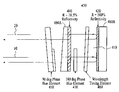
Figure 4 illustrates a preferred embodiment of a nonlinear interferometer in
accordance with the present invention. The interferometer 400 would reside
within a
separator in a DWDM. The interferometer 400 comprises two glass plates 480A-
480B,
creating a space 410 therebetween. The inside face ~of the glass plate 480B is
coated with
a reflective coating 420 with a reflectivity preferably of 100%. The inside
face of the
glass plate 480A is coated with a reflective coating 440 with reflectivity
preferably of
approximately 18%. A phase bias element 430, preferably of 180 degrees, is
placed
between the glass plates 480A and 480B, protruding partially into the space
410. The
180 degree phase bias element 430 will introduce a phase shift of n into the
even
channels of the signal 10 while maintaining the phase of the odd channels in
signals 10
and 20. The phase bias element 450, preferably of 90 degrees, and the
wavelength
tuning element 460 change the shape of the curve of the channels, as will be
described
later.
Figure 5 illustrates one embodiment of a separator which can utilize the
nonlinear
interferometer 400 of the present invention. This embodiment has been
disclosed in U.S.
Patent Application entitled "Fiber Optic Dense Wavelength Division Multiplexes
With
A Phase Differential Method Of Wavelengths Sep~~ration Utilizing Glass Blocks
And A
CA 02327654 2000-10-OS
WO 00151247 PGT/US00/03143
Nonlinear Interferometer," Serial No. ~JAS975P) , filed on Applicant hereby
incorporates this patent application by reference. The separator 500 comprises
an input
fiber 530 for inputting an optical signal, and two output fibers 540 and 560.
It comprises
two lenses 570 and 580 which collimate the input signal as it comes from the
input fiber
530 and converge the output signal to the output fibers 540 and 560. It also
comprises
two blocks of glass 510A-510B placed next to each other. Adjacent to one side
of the
blocks 510A and 5108 is a nonlinear interferometer 400 of the present
invention which
introduces a phase difference into the even channels while maintaining the
same phase
for the odd channels. At the place where the two blocks 510A-5108 meet, the
glass is
coated with a reflective coating 520 with a reflectivity, for example, of 50%.
The reflective coating 520 splits the optical signal containing ~,1 - ?~,"
into at least
two portions 10 and 20. In the preferred embodiment, the reflective coating
520 is
polarization insensitive. The nonlinear interferometer 400 then introduces a n
phase
difference into the even channels of signal 10 which travels through the 180
degree phase
bias element 430 (Figure 4) while maintaining the phase of the odd channels of
signals
10 and 20. The two output fibers 540 and 560 are then aligned, or placed at a
particular
distance from the separator 500, such that even channels are captured in one
fiber while
the odd channels are captured in the other.
Figure 6 illustrates the odd channels of an input signal as it travels through
the
separator 500 which may contain the interferometer 400 of the present
invention. An
input signal (~,~ - ~,") enters the separator 500 through input fiber 530. The
signal travels
through the lens 570 which collimates the signal and directs it toward the
glass blocks
S l0A and 5108. The signal travels through the glass blocks S l 0A and S 108,
and when
it reaches the 50% reflective coating 520, it is split into two signals 20 (-
E1) and 10 (E2).
Signal 20 travels to and back from the interferometer 400 without a change in
its phase.
Signal 10 also travels to and back from the interferometer 400; including the
180 degree
phase bias element 430, but no phase change is introduced into its odd
channels. Thus,
when the odd channels of signals 10 and 20 travel back from the interferometer
400, they
are in phase. The signals 10 and 20 travel through the glass blocks 51 OA and
5108
again. When they reach the 50% reflective coating 520 again, they travel to
the same
location, output fiber 540, which is placed in a position such that the phase
of the odd
channels are captured.
CA 02327654 2000-10-OS
WO 00151247 PCTIUS00/03143
7
Figure 7 illustrates the even channels of an input signal as it travels
through the
separator 500 which may contain the interferometer 400 of the present
invention. The
even channels travel through the separator S00 in same manner as the odd
channels,
described above with Figure 6, however, when the even channels of signal 10
enter the
S interferometer 400, they travel through the 180 degree phase bias element
430 which
introduces a 180° phase change. When the signals 10 and 20 travel back
from the
interferometer 400, their even channels are out of phase. When they reach the
SO%
reflective coating again 520, the even channels with. the phase change travel
to output
fiber 560, which is positioned such that the phase of the even channels are
captured.
The nonlinear interferometer 400 is constructed with a cavity 410 with a 100%
reflecting mirror 480B on one side and phase bias elements 430 and 450 inside
and
outside of the cavity 410. The cavity 410 is basically a well known Gires-
Tournois
etalon. (See "Optical Waves In Crystals" by Amnion Yariv and Pochi-yeh, John
Wiley
and Sons, 1984, p. 291.) Because of the 100% miwor 480B, all the incident
light will be
reflected back by the cavity 410 with a phase shift of reflection ~,
~ _ -2 tan-' 1 + ~ tan ~
1-
where R is the reflectivity of the front mirror 480A, and 2cp is round trip
phase
gain in the cavity 410 given by
2~ L o
Lo being the optical path length of the cavity 410. An additional 180°
phase bias
element 430 is inserted in the cavity 410 for one of beams 10 and 20 only. A
90° phase
bias element 450 is placed outside the cavity 410. Therefore the phase shift
difference
experienced between light from 10 and 20 is the following:
0~ =-2tan-' i+~tan~ +2tan-'I/i+~tan~~+ 2~ - 2
CA 02327654 2000-10-OS
WO 00/51247 PCTNS00/03143
The interference between these twa beams 10 and 20 after they are recombined
by the 50% splitter 520 results in a standard interference intensity pattern.
I1 = I o cos 2 12 = I o sin
2 2
where to is the initial light intensity, l~ is the light intensity directed
toward fiber 540 and
IZ is the light intensity directed toward fiber 560. The spectrum 340 of h is
plotted in
Figure 3. The period between transmission peaks is determined by the optical
length L°
of the cavity 410. The shape of the spectrum however is determined by the
front minor
480A reflectivity R.
The 90 degree bias element 450 and the wavelength tuning element 460 fine tune
the shapes and positions of the pass bands and isolation bands to their
desired properties.
To illustrate the advantage of flattening the curve tips and allowing a small
I S amount of band-shape distortion, please refer back to Figure 3. Figure 3
is a graph of
spectrum curve 310 of a signal which would result if the reflective coating
440 has a
reflectivity of 0%. This curve 310 has no crosstalk but has a very narrow
isolation band
330 and a narrow pass band 320. The spectrum curve 340 is a signal which would
result
if the reflective coating 540 has a reflective index of approximately 18%.
There is a
small amount of band-shape distortion 350 and the isolation band 360 is
significantly
wider. In addition, the tips of the curve are flatter, resulting in a wider
pass band 370.
The amount of flattening and band-shape distortion allowed can be manipulated
by
selecting a reflective coating with a certain reflectivity. Thus, the
separator 500, through
manipulation of its interferometer 400 of the present invention, can be used
to broaden
the pass and isolation bands, which makes the curve more stable and tolerant
to drift.
Figure 8 illustrates a second preferred embodiment of an interferometer in
accordance with the present invention. The interferometer 800 comprises two
glass
plates 880A and 880B. The inside face of the glass plate 880B is coated with a
layer of
reflective coating 820 with a reflectivity preferably of 100%. The inside face
of the
glass plate 880A is coated with a layer of reflective coating 840 with a
reflectivity
preferably of approximately 18%.
When signal 30 enters the interferometer 800, it passes through the 18%
CA 02327654 2000-10-OS
WO 00/51247 PCT/US00/03143
reflective coating 840 and a waveplate 895 preferably of 7~,/4.
The polarization splitting interferometer 800 is similar to the beam splitting
interferometer 400, except the ~./4 plate 895 introduces an 180° round
trip phase change
between a o beam and a beam of the signal inside the cavity 810, and the
external 7~.I8
S plate 890 introduces the round trip 90° phase change: between the o
beam and a beam.
The waveplate 890, preferably of 7~J8, fine tunes the shape of the signal 30
in the
same manner as the 90 degree phase bias element 4~>0 (Figure 4) of the first
preferred
embodiment.
The second preferred embodiment of the intc;rferometer 800 as illustrated in
Figure 8 is temperature sensitive. The rear glass plate 880B and the waveplate
895 will
expand/contract with changes in temperature. These expansions/contractions
will change
the length of separation between them, varying the l:unctioning of the
interferometer 800.
Figure 9 illustrates a third preferred embodiment of the interferometer in
accordance with the present invention. The interferometer 900 is the same as
the
interferometer 800 except the two glass plates 880A-880B are set apart by zero
expansion cavity spacers 910, creating a main cavity 920. The zero expansion
cavity
spacers 910 are composed of a temperature insensitive material so they do not
expand/contract with changes in temperature. A back mirror 930 is attached to
the glass
plate 880B. In this embodiment, the reflective coating 820 is on the back
minor 930
rather than the glass plate 880B. Although the zero expansion cavity spacers
910 keep
the length of the cavity 920 constant, the waveplate 895 and the back mirror
930 may
expand/contract with changes in temperature, varying the functioning of the
interferometer 900. A temperature controller (not shown) may be coupled to the
interferometer 900 so that the expansions of the back mirror 930 and the
waveplate 895
cancel each other out, maintaining a constant distance between them.
Figure 10 illustrates a top view of a preferred embodiment of a separator
which
rnay be used with the second and third preferred embodiments of the
interferometers of
the present invention. For the purpose of describing this separator 1000, an
interferometer with the structure illustrated in Figure 8 is used. The
separator 1000
comprises an optical fiber 1010 for inputting an optical signal and optical
fibers 1020
and 1030 for outputting optical signals. As the siyal leaves the optic fiber
1010, it
diffuses.
CA 02327654 2000-10-OS
WO 00/51247 PCT/US00103143
to
A lens 1050 contains the signal and directs it towards a beam splitter 1070
which
decomposes the signal based upon its polarity. This decomposition takes place
at the
body diagonal junction plane 1075 of the beam splitter 1070. The component (p-
component) of the input signal polarized within the plane defined by the input
signal's
direction of travel and a line perpendicular to junction plane 1075 passes
through beam
splitter 1070 towards an interferometer 8008. The component (s-component) of
the
input signal polarized parallel to junction plane 1075 passes trough beam
splitter 1070
towards an interferometer 800B. The interferometers 800A and 8008 introduce
phase
differences between the even and odd channels of the signals.
Figure 11 illustrates the path of the odd channels as they travel through the
separator 100 with the interferometer 800A and 8008 of the present invention.
The odd
channels travel to the polarization beam splitter 1070 from the input fiber
1010. Each
channel has an s polarity component (E,) 1110 and a p polarity component (EP)
1120.
The E, and EP signals may each be decomposed into Eo and E~ components
parallel to
the principal ray directions of the birefringent elements in interferometer
8008 and
800A, respectively. These components are well known in the art and will not
further be
described here. The vector EP 1120 is decomposed into components E~ 1130 and
Ep
1140 whereas the vector E, 1110 is decomposed into components E,o 1150 and Ex
1160.
This decomposition is illustrated in Figure 11 for each of the signal
polarization
component vectors E, and EP both before its entry into and after its exit from
the
interferometer 800A and 8008, respectively. The signal EP 1120 travels to the
interferometer 8008 while E, 1110 travels to interferometer 800A. Both sets of
signals
are reflected by their interferometers 800A and 8008 without a phase shift
difference
between E,o 1150 and E,e 1160 (or between EPo 1130 and EPA 1140). Thus, both
the
signal EP 1120 and the signal E, 1110 travel back to the polarization beam
splitter 1070
without a change in orientation. These signals then travel back through the
polarization
beam splitter 1070 to output fiber 1020.
Figure 12 illustrates the path of the even channels as they travel through the
separator 1000 with the interferometer 800A and 8008 of the present invention.
As with
the odd channels, the even channels travel to the polarization beam splitter
1070 from the
input fiber 1010. Each channel has an s polarity component {E,) 1210 and ap
polarity
component (EP) 1220. As with the odd channels, the E, and EP signals may each
be
CA 02327654 2000-10-OS
WO 00/51247 PGTlUS00/03143
decomposed into Eo and E~ components parallel to the principal ray directions
of the
birefringent elements in interferometer 800A and 80~OB, respectively. The
vector EP
1220 is decomposed into components EPo 1230 and :EPA 1240 whereas the vector
ES 1210
is decomposed into components Eso 1250 and Es~ 1260. This decomposition is
illustrated
in Figure 12 for each of the signal vectors Ef and EP both before its entry
into and after
its exit from the interferometer 800A and 800B, respectively. The signal EP
1220 travels
to the interferometer 800B while the signal Es 1210 travels to interferometer
800A. Far
the even channels, interferometers 800A and 800B introduce a n phase
difference
between EPo 1230 and EP~ 1240 and also between E~ 1250 and ES~ 1260
respectively.
This phase difference causes an effective n/2 rotation of each of the signals
1210 and
1220, thereby converting them from E, into E~ and from EP into E,,
respectively. When
both of these signals travel through beam splitter 1070 again, this rotation
causes them to
travel to output fiber 1030. Thus, in this manner, output fiber 1020 contains
the odd
channels while output fiber 430 contains the even channels.
A nonlinear interferometer separation mechanism for use within a dense
wavelength division multiplexes has been disclosed.. The nonlinear
interferometer allows
a dense wavelength division multiplexes to have an ease in alignment and a
higher
tolerance to drifts due to the increase in the width of the pass band. It also
has the added
ability of being passively stable to temperature.
Although the present invention has been described in accordance with the
embodiments
shown, one of ordinary skill in the art will readily recognize that there
could be
variations to the embodiments and those variations would be within the spirit
and scope
of the present invention. Accordingly, many modifications may be made by one
of
ordinary skill in the art without departing from the spirit and scope of the
appended
claims.