Language selection

Search

Patent 2327977 Summary

Third-party information liability

Some of the information on this Web page has been provided by external sources. The Government of Canada is not responsible for the accuracy, reliability or currency of the information supplied by external sources. Users wishing to rely upon this information should consult directly with the source of the information. Content provided by external sources is not subject to official languages, privacy and accessibility requirements.

Claims and Abstract availability

Any discrepancies in the text and image of the Claims and Abstract are due to differing posting times. Text of the Claims and Abstract are posted:

  • At the time the application is open to public inspection;
  • At the time of issue of the patent (grant).
(12) Patent: (11) CA 2327977
(54) English Title: LOW PIM COAXIAL DIPLEXER INTERFACE
(54) French Title: FAIBLE MODULE D'INTERFACE DIPLEXEUR COAXIAL D'INTERMODULATION PASSIVE (IMP)
Status: Expired and beyond the Period of Reversal
Bibliographic Data
(51) International Patent Classification (IPC):
  • H01P 5/08 (2006.01)
  • H01P 1/213 (2006.01)
(72) Inventors :
  • HENDRICK, LOUIS W. (United States of America)
  • REYNOLDS, ROBERT L. (United States of America)
  • KICH, ROLF (United States of America)
(73) Owners :
  • THE BOEING COMPANY
  • COM DEV INTERNATIONAL LTD.
(71) Applicants :
  • THE BOEING COMPANY (United States of America)
  • COM DEV INTERNATIONAL LTD. (Canada)
(74) Agent: SMART & BIGGAR LP
(74) Associate agent:
(45) Issued: 2003-11-11
(22) Filed Date: 2000-12-08
(41) Open to Public Inspection: 2001-06-09
Examination requested: 2000-12-08
Availability of licence: N/A
Dedicated to the Public: N/A
(25) Language of filing: English

Patent Cooperation Treaty (PCT): No

(30) Application Priority Data:
Application No. Country/Territory Date
09/458,260 (United States of America) 1999-12-09

Abstracts

English Abstract

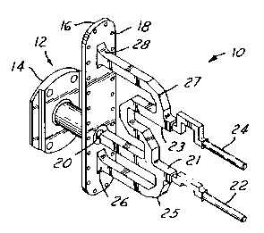
A common interface (10) for a PIM sensitive diplexing filter (30) is provided in a non- contacting, or isolated, configuration while providing PIM reliability, ESD conduction and thermal conduction, making it ideal for high power space applications. The common interface (10) is a one- piece construction of a diplexed, or multiplexed, coaxial, or squareax, transmission line that is constructed with a direct non-contacting (34, 36), or connectionless, interface. Terminations (26, 28) connect the inner conductor (20) to the outer conductor (12) of the interface (10) making the device one integral piece yet providing the necessary isolation through non-contacting interface with a PIM sensitive device and terminations (26, 28) that provide thermal and ESD conduction necessary for PIM reliablity.


French Abstract

Une interface commune (10) pour un filtre de diplexage (30) sensible à une IMP est fournie dans une configuration sans contact, ou isolée tout en fournissant une fiabilité IMP, la conduction de DES et la conduction thermique, la rendant idéale pour des applications spatiales à haute puissance. L'interface commune (10) est une construction en une seule pièce d'une ligne de transmission diplexée, ou multiplexée, coaxiale, ou quadriaxe qui est construite avec une interface sans contact direct (34, 36), ou sans connexion. Les terminaisons (26, 28) relient le conducteur intérieur (20) au conducteur extérieur (12) de l'interface (10) formant le dispositif intégralement dans une seule pièce fournissant l'isolation nécessaire par le biais d'une interface sans contact avec un dispositif sensible à l'IMP et des terminaisons (26, 28) qui fournissent une conduction thermique et de DES nécessaire pour la fiabilité IMP.

Claims

Note: Claims are shown in the official language in which they were submitted.


9
What Is Claimed Is:
1. An interface for a PIM sensitive
device, said interface comprising:
a cane-piece integrated configuration
for inner and outer conductors, said one-piece
configuration having predefined paths for
providing direct electrical and thermal
conduction therebetween.
2. The interface as claimed in claim
1 further comprising a flange member for
connection to said PIM sensitive device.
3. The interface as claimed in claim
2 wherein said flange member further comprises
fastening members for a high-pressure interface.
4. The interface as claimed in claim
2 wherein said inner conductor branches into a
plurality of terminations, at least one of which
connects to said outer conductor at said flange
member.
5. The interface as claimed in claim

10
1 wherein said inner conductor and said PIM
sensitive device are connected by at least one
non-contacting choke joint.
6. The interface as claimed in claim
4 wherein said inner conductor further comprises
at least one branch from said inner conductor to
said flange member such that a short circuit is
provided for thermal and ESD conduction.
7. The interface as claimed in claim
4 wherein said inner conductor further comprises
at least one branch from said inner conductor
away from said flange member to provide an open
circuit to said PIM sensitive device.
8. The interface as claimed in claim
7 wherein said at least one branch further
comprises a branch for a transmit band and a
branch for a receive band.
9. The interface as claimed in claim
7 wherein said at least one branch extending
away from said inner conductor is coupled to
said PIM sensitive device by way of a choke

11
joint.
10. The interface as claimed in claim
7 and further comprising at least one branch for
coupling to a transmit filter section and at
least one branch for coupling to a receive
filter section.
11. The interface as claimed in claim
10 wherein said couplings are non-contacting
choke joints.

Description

Note: Descriptions are shown in the official language in which they were submitted.


CA 02327977 2000-12-08
Technical Field
The present invention relates to a PIM
sensitive diplexing or multiplexing filter and more
particularly to an interface for the coaxial common
5 port of a diplexing or multiplexing filter.
Background Art
A common coaxial transmission line must be
connected to the resonating elements of a filter
section in such a manner as to reliably avoid the
10 production of passive intermodulation (PIM). The
highest reliability in the avoidance of PIM is
accomplished by coupling the transmission line and
the filter in a non-contacting, or "isolated"
configuration, i.e. a capacitive joint and/or an
15 inductive joint. However, while this electrical
isolation avoids PIM, it introduces other problems.
For example, there is no bleed path for electrostatic
charge build-up. Another potential problem is a
build up of heat from poor heat dissipation of the
20 inner conductor because there are no conduction paths
that are inherent with "directly" contacting
conductors.
In an attempt to overcome these problems, a
thermal shunt, or other thermally conductive path
25 consisting of a direct electrical and thermally

CA 02327977 2003-05-22
2
conductive path between the inner conductor and the
outer conductor :has been added to the interface.
This requires that the :inner conductor of the PIM
sensitive hai:°d~ware must be intimately attached to
5 the outer conductor. At least one fastening
attachment , ::~u.ch as a screw, is normally used .
Unfortunately, this assembly is not very reliable in
terms of PIM :~v~oidance .
10 The:~e~ :is a need for a PIM sensitive
diplexing-fili~e~r. common interface that provides PIM
reliability i.n conjunction with ESD conduction and
thermal dissip<~ti~on, making it ideal for high power
space applications.
15
;summary Of The Invention
In one aspect of the present invention,
there is pro~~~~ided one-piece interface connector for
a PIM sensit.i~ve diplexing filter. In the present
20 inver.~tion there is an absence of contacting
connections o.f the inner-conductor. The inner-
conductor and outer-conductor are one piece, thereby
eliminating any direct metal-to-metal connections to
the high cur~.ent carrying inner-conductor. The only
25 direct connect:ion is to t:he outer-conductor that can

CA 02327977 2003-05-22
3
be c~~nnected by any means proven to have high
reliability i~:u the' avoidance of PIM generation, such
as a high-pressure' connection.
5 In one aspect, the present invention
allows the transfer of high power RF energy from the
resonating elerneni~ of a cavity resonating filter to
another compor,~e~nt , such as an antenna feed element .
The transfer :i:~ such that it avoids the risk of PIM
10 generation wr:~ile providing a thermally conductive
path and are electrostatic conductive path to
dissipate heal:: and dissipate static electric charges
from the tran;~mi.ssion line inner conductor.
15 The inner-conductor of the interface is
integral with 'the outer-conductor of the interface,
thereby eliminating any need to connect the inner-
conductors of the interface to the outer conductor.
The outer-conductor of the interface has flange, or
20 other structu.r~e, which allows for a connection to
the outer-conductor of a transmission line or filter
housing. The :result is a "one-piece" construction of
a diplexed, (or mul.tiplexed), coaxial, (or
squareax) , t:~-ar~smission line so as to provide a
25 direct path for thermal dissipation and ESD

CA 02327977 2003-05-22
3a
ground and having a non-contacting, integral inner-
conductor interf:ac:e .
In accordance with another aspect of the
5 present inven.t.ian, there is provided an interface
for a PIM sensitive device, said interface
comprising:
a an~e-piece integrated configuration for
inner and outer conductors, said one-piece
10 configuration having predefined paths for providing
direct elect:ric~al and thermal conduction
therebetween.
It is an object of an aspect of the
15 present invention to transfer high power RF energy
from a resonalr.i.ng filter to another component. It is
another abject: of an aspect of the present invention
to avoid the risk of passive intermodulation
generatian. Ivy is yet another object of the present
20 invention to provide a conductive path to dissipate
heat and stat:i.c electric charges.

CA 02327977 2000-12-08
- 4 -
Other objects and features of the present
invention will become apparent when viewed in light
of the detailed description of the preferred
embodiment when taken in conjunction with the
5 attached drawings and appended claims.
Brief Description of the Drawings
In order that the invention may be well
understood, there will now be described some
embodiments thereof, given by way of example,
10 reference being made to the accompanying drawings, in
which:
FIGURE 1 is a perspective view of a coaxial
diplexer interface of the present invention; and
FIGURE 2 is a cross-sectional view of the
15 coaxial diplexer interface of the present invention
in communication with a filter housing.
Best Models) For Carrying Out The Invention
Figure 1 is a perspective view of the low
passive intermodulation (PIM) coaxial diplexer
20 interface 10 of the present invention. It should be
noted that while the present invention is being
described herein in conjunction with a diplexed
coaxial transmission line, it is possible to
incorporate the present invention with a multiplexed
25 coaxial or squareax transmission line as well. One

CA 02327977 2000-12-08
- 5 -
of ordinary skill in the art will have knowledge
sufficient, in conjunction with the information in
the present disclosure, to apply the present
invention to the multiplexed coaxial or squareax
5 transmission line application.
An outer conductor 12 of the interface 10
has a common port 14 and a flange member 16 having
structure 18 for receiving a high-pressure interface
(not shown). Integral to the outer conductor 12 is
10 an inner conductor 20.
The inner conductor 20 has several branches
21, 23, 25 and 27, leading to terminations of the
inner conductor 20. The first branch 21 leads to a
non-contacting coupling with a resonating element of
15 a section of a PIM sensitive device (not shown) by
way of a quarter wavelength coupling probe 22.
Branch 23 leads to a non-contacting coupling with a
resonating element of another section of the PIM
sensitive device (not shown) by way of probe 24.
20 Branches 25 and 27 lead to terminations 26
and 28 at the flange 16 making the inner conductor 20
and the outer conductor 12 an integral piece. The
terminations 26 and 28 provide the necessary
isolation and at the same time provide the electrical
25 and thermal conduction required for PIM reliability.

CA 02327977 2000-12-08
- 6 -
Because the terminations 26 and 28 are
integral to the flange member 16, it is possible to
manufacture the inner and outer conductors as one
integral part, as for example, by a machining
5 process. The terminations 26 and 28 provide a direct
thermal dissipative path and ESD ground. The
branches 21 and 23 provide a connectionless interface
with a PIM sensitive device (not shown).
Figure 2 is a cross-sectional view of the
10 interface 10 of the present invention in
communication with a PIM sensitive filter 30. Only
non-contacting connections are present at the inner
conductor branches 21 and 23 by way of probes 22, 24.
The only direct connection is provided at
15 the outer conductor 12 of the interface 10 where it
is connected at the flange 16 with a high pressure
fitting 31. It is known that a high-pressure
interface of 10 kPSI provides a reliable PIM
avoidance connection, a good thermal conduction path,
20 and a good ESD conduction path. It is possible,
however, to substitute the high pressure interface
shown with another suitable connection method.
The various connections of the interface 10
are connected to the filter 30 in the following
25 manner. A first resonating element 32 of the
transmit filter section is coupled to probe 22 by way
of a non-contacting choke joint. In a choke joint,

CA 02327977 2000-12-08
_ 7
the surface of the connection is covered with a
dielectric material 34 to isolate the connection,
making it non-contacting. The first resonating
element 36 of the receive filter section is also
5 coupled to the inner conductor 20 by the second probe
24, also by way of a choke joint isolated by
dielectric material 38. The first and second probes
24, 22 maintain a length, or phase, relationship such
that the transmit and receive filter sections are
10 multiplexed at a termination 40 of the inner
conductor 20. The termination 40 is coupled to an
antenna element, (not shown), also by a choke joint.
The terminations 26 and 28 of the inner
conductor 20 are directly integrated to the outer
15 conductor 12 in a one-piece construction as described
above. The terminations 26 and 28 maintain a length,
or phase, relationship such that an "open" circuit
appears respectively at transmit and receive bands,
yet maintains a short circuit for thermal conduction
20 from the inner conductor 20 and ESD conduction to the
outer conductor 12.
Using a high-pressure interface 31, the
outer conductor of the filter housing 30 is directly
connected to the outer conductor of the coaxial
25 diplexer interface 12, yet the inner conductor 20 is
connectionless, thereby avoiding the generation of
any PIM through direct connections.

CA 02327977 2000-12-08
_ g _
While particular embodiments of the
invention have been shown and described, numerous
variations and alternate embodiments will occur to
those skilled in the art. Accordingly, it is
5 intended that the invention be limited only in terms
of the appended claims.

Representative Drawing
A single figure which represents the drawing illustrating the invention.
Administrative Status

2024-08-01:As part of the Next Generation Patents (NGP) transition, the Canadian Patents Database (CPD) now contains a more detailed Event History, which replicates the Event Log of our new back-office solution.

Please note that "Inactive:" events refers to events no longer in use in our new back-office solution.

For a clearer understanding of the status of the application/patent presented on this page, the site Disclaimer , as well as the definitions for Patent , Event History , Maintenance Fee  and Payment History  should be consulted.

Event History

Description Date
Time Limit for Reversal Expired 2017-12-08
Letter Sent 2016-12-08
Letter Sent 2015-08-06
Appointment of Agent Requirements Determined Compliant 2009-04-16
Inactive: Office letter 2009-04-16
Revocation of Agent Requirements Determined Compliant 2009-04-16
Letter Sent 2009-01-20
Revocation of Agent Request 2008-12-23
Appointment of Agent Request 2008-12-23
Letter Sent 2008-07-30
Inactive: Office letter 2006-12-05
Inactive: Payment - Insufficient fee 2006-12-04
Inactive: Late MF processed 2006-11-17
Inactive: IPC from MCD 2006-03-12
Inactive: Office letter 2006-01-26
Letter Sent 2005-12-08
Grant by Issuance 2003-11-11
Inactive: Cover page published 2003-11-10
Pre-grant 2003-08-20
Inactive: Final fee received 2003-08-20
Amendment After Allowance Requirements Determined Compliant 2003-06-11
Letter Sent 2003-06-11
Inactive: Amendment after Allowance Fee Processed 2003-05-22
Amendment After Allowance (AAA) Received 2003-05-22
Notice of Allowance is Issued 2003-02-20
Letter Sent 2003-02-20
Notice of Allowance is Issued 2003-02-20
Inactive: First IPC assigned 2003-01-31
Inactive: Approved for allowance (AFA) 2003-01-31
Inactive: IPC removed 2003-01-31
Amendment Received - Voluntary Amendment 2001-11-09
Letter Sent 2001-09-20
Inactive: Office letter 2001-09-20
Inactive: Multiple transfers 2001-08-09
Application Published (Open to Public Inspection) 2001-06-09
Inactive: Cover page published 2001-06-08
Inactive: First IPC assigned 2001-02-26
Inactive: Courtesy letter - Evidence 2001-01-23
Inactive: Filing certificate - RFE (English) 2001-01-19
Filing Requirements Determined Compliant 2001-01-19
Application Received - Regular National 2001-01-18
Request for Examination Requirements Determined Compliant 2000-12-08
All Requirements for Examination Determined Compliant 2000-12-08

Abandonment History

There is no abandonment history.

Maintenance Fee

The last payment was received on 2002-11-25

Note : If the full payment has not been received on or before the date indicated, a further fee may be required which may be one of the following

  • the reinstatement fee;
  • the late payment fee; or
  • additional fee to reverse deemed expiry.

Please refer to the CIPO Patent Fees web page to see all current fee amounts.

Owners on Record

Note: Records showing the ownership history in alphabetical order.

Current Owners on Record
THE BOEING COMPANY
COM DEV INTERNATIONAL LTD.
Past Owners on Record
LOUIS W. HENDRICK
ROBERT L. REYNOLDS
ROLF KICH
Past Owners that do not appear in the "Owners on Record" listing will appear in other documentation within the application.
Documents

To view selected files, please enter reCAPTCHA code :


To view images, click a link in the Document Description column. To download the documents, select one or more checkboxes in the first column and then click the "Download Selected in PDF format (Zip Archive)" or the "Download Selected as Single PDF" button.

List of published and non-published patent-specific documents on the CPD .

If you have any difficulty accessing content, you can call the Client Service Centre at 1-866-997-1936 or send them an e-mail at CIPO Client Service Centre.


Document
Description 
Date
(yyyy-mm-dd) 
Number of pages   Size of Image (KB) 
Representative drawing 2001-06-04 1 11
Description 2000-12-08 8 232
Description 2003-05-27 9 252
Claims 2003-05-27 3 58
Cover Page 2003-10-08 1 45
Drawings 2000-12-08 1 29
Abstract 2000-12-08 1 21
Claims 2000-12-08 3 58
Cover Page 2001-06-04 1 40
Filing Certificate (English) 2001-01-19 1 164
Courtesy - Certificate of registration (related document(s)) 2001-09-20 1 137
Reminder of maintenance fee due 2002-08-12 1 114
Commissioner's Notice - Application Found Allowable 2003-02-20 1 160
Maintenance Fee Notice 2006-02-02 1 172
Notice of Insufficient fee payment (English) 2006-12-04 1 94
Late Payment Acknowledgement 2006-12-05 1 166
Maintenance Fee Notice 2017-01-19 1 179
Maintenance Fee Notice 2017-01-19 1 178
Correspondence 2001-01-19 1 24
Correspondence 2001-09-20 1 12
Correspondence 2003-08-20 2 88
Correspondence 2006-01-26 1 19
Correspondence 2006-12-05 1 27
Correspondence 2006-12-05 1 13
Correspondence 2008-12-23 5 117
Correspondence 2009-04-16 1 13
Correspondence 2009-04-16 1 16