Note: Descriptions are shown in the official language in which they were submitted.
CA 02328587 2000-12-15
MODULAR ELECTROMAGNETIC SENSING APPARATUS
FIELD OF THE INVENTION
This invention relates to electromagnetic sensing apparatus and in
particular to a method and apparatus for the non-contacting measurement of
earth
material electrical and magnetic properties with respect to depth below
surface and
position.
BACKGROUND OF THE INVENTION
Portable devices currently available for in-situ direct estimation of nearby
earth materials' apparent conductivity will be referenced in the following as
terrain
conductivity meters (TCM's) and multi-frequency EM sounders (MEMS). Extensions
to
the TCM approach, which will be referenced as the ground conductivity meter
(GCM)
and array conductivity meter (ACM), improve aspects of TCM operation.
TCM's
The first devices which could be described as TCM's were described by
Doll (Doll, H.G., 1949, Introduction to Induction Logging and Application to
Logging of
Wells Drilled with Oil Base Mud, J. Pet. Technol. 1, pp 148-162) in a borehole
context
and Howell (Howell, M., 1966, A Soil Conductivity Meter, Archaeometry 9, pp.
20-23)
in a shallow soil conductivity measurement context. Examples of commercially-
-1-
CA 02328587 2009-05-15
available TCM's include the Geonics Ltd. EM-31, EM-34 and EM-38 and the
Geofizyka
CM-031. These devices use the Low Induction Number Approximation (LINA) to
estimate the apparent conductivity of the earth materials over a range of
depths by a
linear scaling operation from the component of the reflected EM signals which
are in
quadrature (i.e. at a 900 phase shift) with the primary field emitted by the
sensor's
transmitter coil. The component of the EM measurement arising from signals in
phase
with the primary field from these devices may also be interpreted, with some
effort, in
terms of apparent conductivity, as well as the apparent magnetic permeability
of the
earth materials under test. The terms apparent conductivity and apparent
magnetic
permeability are defined below.
Existing TCM's incorporate a transmitter coil transmitting a sinusoidal
signal at a single stable frequency (e.g. approximately 10 kHz for the EM-31)
such that
the LINA holds, i.e. that the following inequality is true:
[(W p Qo )'/2 p ] < 0.5,
where w is the operating frequency in radians/sec, p is the magnetic
permeability of
the earth in henrys/metre, Qo is the conductivity of the earth in Siemens/m,
and p is the
separation in metres between the transmitter and receiver coils (as described
further
below).
In a TCM, a receiver coil is located at a distance p from the transmitter
coil and substantially coplanar with the transmitter coil. There may or may
not be a
preamplifier located near this receiver coil to increase its effective output
signal level.
-2-
CA 02328587 2000-12-15
The peak moment (transmitter coil current times number of turns time area of
one
turn) of the transmitter coil's magnetic field is such that an acceptable
signal to noise
ratio (SNR) can be obtained at the receiver.
TCM's also incorporate electronics which can analyse the signal picked
up at the receiver coil into components in phase and in quadrature (90 degrees
out of
phase) with the transmitted field. The quality of calibration of the output of
this
process and its stability are important factors in the utility of the
instrument. These
electronics also include circuits and/or software which convert the measured
quadrature component into an apparent resistivity using the LINA relationship
as
stated in McNeill (McNeill, J.D., 1980, Electromagnetic Terrain Conductivity
Measurement at Low Induction Numbers, Technical Note TN-6, Geonics Limited,
Mississauga, Canada) after Wait (Wait, J.R., 1962, A Note on the
Electromagnetic
Response of a Stratified Earth, Geophysics 27, pp 382-385.), i.e.
Qa = 4/(W p p 2) * (Hs/Hp)quadrature
The fundamental unit of apparent conductivity under the MKS system of
units is Siemens/meter (S/m), although most if not all TCM's present their
quadrature
data in terms of milliSiemens/m. In situations displaying horizontally-layered
geology,
the apparent conductivity represents a weighted average of the earth
materials'
conductivity in the vicinity of the sensor. A commonly-accepted rule-of-thumb
depth of
investigation (DOI) has been defined by McNeill as 1.5 times the transmitter-
receiver
separation for the horizontal coplanar configuration and 0.75 times this
separation for
-3-
CA 02328587 2000-12-15
the vertical coplanar configuration, corresponding to a cumulative response
value of
approximately 30%. Using the same 30% value for the perpendicular
configuration's
cumulative response yields a DOI for this configuration of approximately 0.5
times the
transmitter-receiver separation.
A separate data logging device is typically provided which can acquire,
store and display the analog outputs of typical commercial TCM's on demand or
at a
preset sampling rate.
The Transmitter and Receiver coils are typically installed near the ends
of a tubular boom or other support structure, while the electronics and data
logging
device are mounted in a package near the central point of the support
structure. The
boom in the EM-31 is designed to be partially disassembled for shipping, with
the two
outer portions attached via couplings to the central portion of the boom,
which is
affixed to the electronics package. Short-offset systems like the EM-38 are
housed in
unitary support structures which incorporate the receiver electronics. The EM-
34 does
not incorporate a rigid housing joining the transmitter and receiver.
The orientation of the Transmitter and Receiver coils is such that the axis
of each coil is approximately vertical when the instrument is held in an
upright position
(the Horizontal Coplanar orientation).
TCM's incorporating horizontal coplanar coil geometries can be rotated
90 degrees about a line joining the Transmitter and Receiver coils to place
the coils
into the Vertical Coplanar orientation, wherein the axes of the coils are
horizontal. As
-4-
CA 02328587 2000-12-15
described above, this approximately halves the effective DOI for the system,
and
allows the user to investigate vertical variations in the conductivity
structure of the
earth.
The principal shortcomings of the TCM are its single transmitter-receiver
coil pair, which doubles the measurement time per station if two depths of
investigation
are desired at each site, its substantial weight (12.4 kg for the EM-31), its
weak joint
structure (for the EM-31), which permits substantial sag and flexibility in
the boom
when assembled, and its bulky packaging which generates uncomfortable
magnitudes
and directions of pressure on the operator's shoulder. TCM's which rely
exclusively
on the LINA formula quoted above for estimation of earth material conductivity
will
generate erroneous values when used under very conductive conditions.
MEMS
A related class of non-contacting multi-frequency electromagnetic
sounders (MEMS) used for near-surface earth material investigation measure the
variation in the instrument's electromagnetic coupling with earth materials as
a
function of frequency. Examples of such instruments include airborne
electromagnetic
(AEM) sensors developed by various companies over the years, including
Barringer
Research, Dighem, Geotech, Geoterrex, Geophex, and Aerodat, and ground systems
such as the Apex Double-Dipole T" and the Geophex GEM-2 T'" and Geophysical
Survey Systems' GEM-300T"" which operate in the range 330 to 20,000 Hz.
-5-
CA 02328587 2000-12-15
Conventional AEM sensors have been thoroughly described in the
literature (e.g. Palacky and West, 1987). Over the last fifteen or twenty
years, efforts
have been made to increase the quantitative capabilities of some AEM sensors
through improvements to calibration methodologies and the introduction of
electronic
calibration methods. These efforts achieved encouraging, though not
definitive,
results. The multi-frequency, rigid-boom approach used in helicopter
electromagnetics
(HEM) received the most attention in terms of calibration. In their simplest
form, HEM
sensors incorporate a linear coil array consisting of a transmitter, a
receiver of
effective area (turns times single-turn area) A, and a bucking coil possessing
an
effective area Ap3, where p is the relative position of the center of the
bucking coil
between the center of the transmitter (at p=0) and the center of the receiver
coil (at
p=1). The bucking coil is connected in opposition to the receiver coil, so
that the
signal induced in the combined receiver-bucking coil circuit by the primary
field
generated by the transmitter is reduced to approximately zero. The secondary
EM
signal, due to eddy currents induced in nearby electrically conductive media
by the
primary field, is the quantity to be measured by the sensor array. This
bucking method
reduces the dynamic range requirements placed on the amplification and signal-
processing electronics used to acquire and analyse the secondary EM signal.
The method, as described to this point, is the same for narrowband or
wideband HEM sensors. Narrowband sensors transmit sinusoidal signals at one
frequency per set of transmitter, receiver and bucking coils, so that multiple-
frequency
-6-
CA 02328587 2000-12-15
measurements require multiple sets of these coils. Wideband sensors broadcast
a
more complicated waveform, which includes many frequency components. The
amplitude and phase of the secondary signal (defined with respect to the
amplitude of
the primary signal at the receiver location) are, in most narrowband
implementations,
measured through analogue or digital synchronous demodulation of the signal
using
analog signal processors, where the phase reference for the demodulation
process is
obtained from a reference coil positioned near the transmitter coil. The
amplitude
information present in the phase reference signal is discarded by conventional
HEM
signal processor units.
In wideband sensors, the bucked signal is typically digitized and either
stacked (i.e. each period of the waveform is added together to yield a stacked
waveform as described by Becker and Cheng (1987), or stored in memory for
later
analysis. A reference waveform representative of the primary field is also
normally
stacked or stored. The stacked or stored waveforms are then subjected to
Fourier
deconvolution, in which the Fourier transform components of the signal
waveform are
divided by the corresponding components of the reference waveform. For
example, in
the GEM-300T"" ground EM sensor, the bucked signal and the reference (obtained
from the bucking coil) are digitised into parallel data streams. The EM
response at
each operating frequency is computed through convolution with cosine and sine
data
series at that frequency (effectively the computation of Discrete Fourier
Transformation
coefficients for these frequencies), followed by correction for amplifier
gains, coil
-7-
CA 02328587 2000-12-15
geometry and the amplitude and phase of the transmitted signal measured using
the
reference signal (Won, I.J., D.A. Keiswetter, G.R.A. Fields, and L.C. Sutton,
1996,
GEM-2: A New Multifrequency Electromagnetic Sensor, JEEG 1, pp. 129-137). The
resulting EM response data are either recorded directly or converted to an
apparent
conductivity value through a transformation relating EM response to the
product of
apparent conductivity and frequency (Won et al, 1996). The GEM-300T"'
instrument
reportedly suffers from deficiencies in calibration and zero-level stability,
which make it
difficult to use their measurements for quantitative layered-earth
interpretation
(Nyquist, Sageep reference). It also lacks the frequency range necessary for
unambiguous resolution of earth material property layering within the first
two metres
below surface except in extraordinarily conductive conditions (McNeill,
Geonics TN30).
For example, at an operating frequency of 1 MHz (about 50 times higher than
its
actual maximum frequency), such an instrument could not resolve layered
structures
smaller than about 1 metre, even in extremely conductive 0.2 S/m earth
materials.
GCM
The ground conductivity meter as defined here is an extension to the
basic horizontal-coplanar geometry TCM through the addition of a second
receiver coil
mounted at right angles to the first one so that this axis of this second coil
precisely
intersects the transmitter coil. An instrument incorporating such a receiver
coil in
addition to a horizontal-coplanar (HCOP) receiver coil is the subject of a
Canadian
-8-
CA 02328587 2000-12-15
Patent 2,142,546 issued April 13, 1999 to Richard S. Taylor and entitled
Apparatus
and Method for Sounding the Earth. This alternative transmitter-receiver
orientation is
known as the Perpendicular Loop configuration (PLC). The output of this PLC
coil is
sensitive to ground conductivity variations to a depth approximately one-third
of that to
which the horizontal coplanar coils are sensitive for a horizontally-
stratified earth
material properties distribution. By using both the HCOP and PLC configuration
outputs, one can simultaneously estimate ground conductivity for two DOI's.
The first
DOI extends to 1.5 times the transmitter-receiver coil spacing for the
horizontal
coplanar coil pair, while the second DOI extends to 0.5 times the coil
separation for the
perpendicular coil pair.
These simultaneous measurements permit continuous EM profiling at two
depths of exploration, an important improvement in terms of productivity over
the TCM.
Another advantage of the PLC extension is that adding a second receiver coil
and its
attendant electronics to a single-transmitter instrument is more efficient in
terms of
power usage and weight, providing a competitive advantage over devices which
seek
to monitor different depth ranges using multiple transmitters and receivers
via MEMS
technology.
SUMMARY OF THE INVENTION
The term Earth materials should be interpreted as inclusive of materials
including but not limited: to soils; rocks; minerals; ores; ice; and solvents
such as
-9-
CA 02328587 2000-12-15
water, brine, pore fluids, ammonia and methane; located on or in the earth or
extraterrestrial bodies including planets, moons, asteroids or comets. Earth
materials
may be characterised by their electromagnetic (EM) properties, i.e. their
electrical
conductivity and permittivity, and their magnetic permeability. The
distribution of these
EM properties with respect to depth and position may be interpreted in terms
of more
geologically or geotechnically useful quantities, including composition,
porosity,
degree of fluid saturation, concentration of salts or other conductive species
in the
solvent, and the concentration of magnetically permeable materials.
This invention provides an improved means for quantitotive estimation of
the electromagnetic properties of earth materials with a lightweight, self-
contained
apparatus. In some embodiments the apparatus is capable of stable extended
operation at low power levels, while in others low-power operation may be
sacrificed
for the sake of reduced noise levels or extended spectral range.
The requirement for quantitative measurement of earth material
properties arises in many applications, most of which lie in the fields of
geotechnical
engineering and environmental assessment, mining, or industrial processes. The
invention will improve the quality and acquisition rate of measurements of the
electromagnetic properties of near-surface earth materials, buried objects,
bodies,
voids or other agglomerations of material of natural or technological origin
possessing
a contrast between their electromagnetic properties and the surrounding
material.
Some particular applications, which may include either surface-based or
-10-
CA 02328587 2009-05-15
low-altitude airborne measurements, include:
= rapid profiling and display of depth-conductivity profiles;
= measurement of the electrical conductivity and thickness of floating ice (or
other
solids) and/or of the underlying water (or other conducting fluid);
= monitoring of soil and/or groundwater salinity for agricultural purposes;
= monitoring of near-surface geology, moisture content, salinity and
electrolyte
= pollution of swamps, marshlands and wetlands;
= searching for objects such as vehicles or structures buried by natural
disasters
such as avalanches and landslides;
= detection of unexploded ordnance;
= detection of underground or underwater storage tanks, pipes, transformers
and
other highly conductive structures; and
= detection of archaeological features such as walls, pits, hearths, floors,
post-
holes, middens, mounds and artifacts;
Accordingly to one aspect of the invention, an electromagnetic sensing
apparatus comprising an electromagnetic transmitter, at least one receiver
device, at
least one calibration device, a switch and a processing means. The
electromagnetic
transmitter generates a transmitter signal. The receiver device is spaced from
the
transmitter, senses a receiver local electromagnetic field proximate thereto
and
generates a receiver signal. The calibration device senses a calibration local
electromagnetic field proximate thereto, generates a calibration signal. The
calibration
-11-
CA 02328587 2000-12-15
device is positioned such that the distance between the transmitter and the
receiver
device is greater than the distance between the transmitter and the
calibration device.
The switch is connected between the receiver device and the calibration
device. The
processing means includes a first input for receiving a signal from one of the
receiver
signal and the calibration signal and a second input for receiving a signal
from the
switch. The processing means compares the first input and the second input and
monitors distortions in the transmitter signal. The sensing apparatus may
include a
plurality of receiver devices in a variety of different configurations.
Accordingly to another aspect of the invention, an electromagnetic
sensing apparatus comprises an electromagnetic transmitter, a first receiver
device, a
second receiver device and a processing means. The electromagnetic transmitter
generates a transmitter signal. The first receiver device is spaced from the
transmitter,
senses a first receiver local electromagnetic field proximate thereto and
generates a
second receiver signal. The second receiver device is spaced from the first
receiver
device, senses a second receiver local electromagnetic field proximate thereto
and
generates a second receiver signal. The processing means has a first input for
receiving the first receiver signal and a second input for receiving the
second receiver
signal. The processing means compares the first input and the second input and
monitors distortions in the transmitter signal.
Accordingly to a further aspect of the invention, a method of analysing
data from electromagnetic sensing apparatus comprises a plurality of steps. A
-12-
CA 02328587 2000-12-15
receiver signal from a receiver device is received and converted into a
complex
receiver signal. Similarly a calibration signal from a calibration device is
received and
the converting signal to a complex calibration signal. The ratio of the
complex receiver
signal to the complex calibration signal is adjusted for the signal processing
components to produce a processing adjusted complex ratio. The processing
adjusted complex ratio is adjusted for the effective areas of the receiver
device and the
calibration device to produced an area adjusted complex ratio. The area
adjusted
complex ratio is adjusted for a distance between the receiver device and a
transmitter
and the distance between the calibration device and the transmitter to produce
a
calibrated field coupling ratio.
Further features of the invention will be described or will become
apparent in the course of the following detailed description.
BRIEF DESCRIPTION OF THE DRAWINGS
The invention will now be described by way of example only, with
reference to the accompanying drawings, in which:
Fig. 1 is a schematic representation of the horizontal positioning of the
coils in the electromagnetic sensing apparatus of the present invention;
Fig. 2 is simplified circuit diagram of the electromagnetic sensing
apparatus of the present invention;
Fig. 3 is a schematic representation of the electromagnetic sensing
-13-
CA 02328587 2000-12-15
apparatus of the present invention relative to the ground;
Fig. 4 is a schematic representation of the horizontal positioning of the
coils in an alternate embodiment of the electromagnetic sensing apparatus of
the
present invention including multiple Receiver Assemblies;
Fig. 5 is a schematic representation of the electromagnetic sensing
apparatus of Fig. 4 relative to the ground;
Fig. 6 is simplified circuit diagram of an alternate embodiment of the
electromagnetic sensing apparatus of the present invention including a
plurality of
receivers an switches;
Fig. 7 is simplified circuit diagram of an alternate embodiment of the
electromagnetic sensing apparatus of the present invention similar to that
shown in
Fig. 6 but also including a plurality of inputs for the calibration signal and
a plurality of
switches.
Fig. 8 is a simplified circuit diagram of the electromagnetic sensing
apparatus of the present invention showing an alternative embodiment of the
calibration technique;
Fig. 9 is a schematic representation in plan view of a two-dimensional
three-Receiver Array Conductivity Meter embodiment of the present iovention;
Fig. 10 is a schematic representation in plan view of a tWo-dimensional
four-Receiver Array Conductivity Meter embodiment of the present invention;
Fig. 11 is a simplified circuit diagram of a two-Receiver Array
-14-
CA 02328587 2000-12-15
Conductivity Meter embodiment of the present invention showing the application
of the
alternative embodiment of the calibration technique to the output-difference
mode of
this array;
Fig. 12 is a simplified circuit diagram of an alternate embodiment of the
electromagnetic sensing apparatus of the present invention similar to that
shown in
Fig. 2 but showing an alternate switching arrangement;
Fig. 13 is a simplified circuit diagram of an alternate embodiment of the
electromagnetic sensing apparatus of the present invention similar to that
shown in
Fig. 2 but showing a simplified switching arrangement; and
Fig. 14 is a simplified circuit diagram of an alternate embodiment of the
electromagnetic sensing apparatus of the present invention similar to that
shown in
Fig. 13 but showing a modified switching arrangement.
DETAILED DESCRIPTION OF THE INVENTION
Fig. 1 depicts a vertical-dipole transmitter coil (Tx) 10, a calibration coil
(Cx) 12, an optional bucking coil (Bx) 14, and a pair of receiver coils Rx
(PLC) 16 and
Rx (HCOP)18. Each of the coils has an axis specifically a transmitter axis 20,
a
calibration axis 22, a bucking axis 24, a receiver PLC axis 26 and a receiver
HCOP
axis 28 respectively. Similarly each of these has an effective center. The
effective
center of a receiver type device, including the Cx 12, Bx 14, Rx PLC 16 and Rx
HCOP
18, may be defined as the centroid of the sensitive region of the receiver
device with
-15-
CA 02328587 2000-12-15
respect to the component of electromagnetic field intensity being sensed by
the
device. The sensitive region is that area or volume of the receiver device
which is
sensitive to the intensity of the electromagnetic field in the vicinity of the
receiver
device. It will be appreciated by those skilled in the art that the centroid
of the sensitive
region is typically substantially coincident with the geometrical center of
the sensitive
region. The effective center of a transmitter device may be defined as the
geometrical
center of the transmitter device.
The HCOP Rx 16 coil is coplanar with the Tx 10 or their effective centres
are coplanar and separated from it by rrx 30. The perpendicular loop coil
(PLC) 18 is
oriented perpendicular to the Tx-Rx plane, with its axis 28 directed toward
the
transmitter coil 10. The PLC 18 and HCOP 16 coils may be concentric or offset.
If
they are offset, the distance between the Tx to the PLC is r,XP which may be
larger or
smaller than rrX. If the Bx coil is present, it is located at rbx 32. The
distance between
the calibration coil 12 and the transmitter 10 is rcx 34 and is less than r,
30
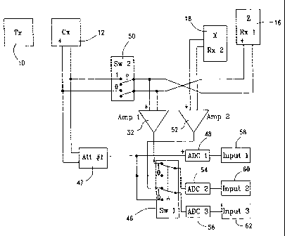
Fig. 2 schematically depicts the first embodiment of the calibration
apparatus. The Cx coil 12 supplies a signal through an anti-alias filter to
certain poles
on Switch #1 46 and directly to an analog to digital converter (ADC) 48. The
output of
this ADC is called the Calibration data stream 58 or input 1. Switch #1
permits the Cx
signal to be applied to the other ADC's when required in order to estalblish
their
calibration factors relative to ADC #1.
A separate pair of leads runs to Switch #2 50 (if present), which is
-16-
CA 02328587 2009-05-15
normally open, but when closed places the Cx coil 12 in opposition to the Rx
coil 16.
Switch #2 50 may be present in the circuit only during initial calibration of
the system,
when it may be used to position the Cx 12 and/or Rx 16 coils and/or to adjust
the
parameters of the Cx 12 and/or Rx 16 coils, such that the combined signal from
the Rx
16 and Cx 12 due to direct pickup of the Tx 10 field is at a minimum. This
methodology allows the Calibration signal emanating from the Cx 12 to be
adjusted so
as to generally match the amplitude and phase of the Rx signal due to direct
pickup of
the Tx field.
Two receiver coils, labelled Z Rx 18 and X Rx 16, are connected via an
amplifier and anti-alias filter 52 to certain poles on Switch #1 46, such that
in position 1
of the switch they are connected through to the second and third ADC's 54 and
56
respectively. The corresponding output data streams of these ADC's are called
the Z
Signal 60 and X signal 62, or inputs 2 and 3 respectively.
Fig. 3 shows the relationship between the Tx 10, Bx 24 (if present) and
Rx coils 36 in a Terrain Conductivity Meter (TCM). In a Ground Conductivity
Meter
(GCM), the single receiver coil labelled Rx 36 would be replaced by a pair of
coils 16
and 18 such as those shown in Figure 2. The array, of length r, 30, is
normally used
with its long axis horizontal at a height h 38 above the ground surface.
Fig. 4 depicts a vertical-dipole transmitter coil (Tx) 10, a calibration coil
(Cx) 12, and multiple receiver assemblies RA140' , RA2 402, and so on to RAm
40m.
These receiver assemblies 40 may include HCOP and/or PLC receiver coils and/or
a
-17-
CA 02328587 2009-05-15
coil oriented at right angles to both of these. For depth sounding purposes,
HCOP and
PLC coils are typically sufficient. The receiver assemblies are located at r,,
r2, ... rm,
421, 42Z, 42"' respectively from the transmitter. If Bx coils were present,
they would be
located at rbx,, rbxZ, ... rbxm (not shown).
Fig. 5 shows the multiple receiver array of Fig. 4 in relation to a layered
earth structure. Each of the Tx-RA pairs samples this structure to a different
set of
DOI values 44, 44'. Suitable choices of Tx-RA distances yields a sensor which
is in
principle capable of providing a continuous profile of earth material
conductivity depth
sections over the range of DOI's provided by the unit as the sensor is moved
over the
earth's surface.
Fig. 6 shows a schematic of a sensing apparatus that includes a plurality
of receiver devices 16 which may each be spaced differently from the
transmitter. The
range of spacings present provides a range of depths of investigation of the
apparatus
in its depth sounding application. Switches Sw 1 64 to Sw n 64" permit the
routing of
signals from receiver devices 1 to n to Inputs 2 66' to n+1 66" during normal
operation,
and from the calibration device to one, two or all of Inputs 1 to n+1 so that
the relevant
Input may be calibrated relative to Input 1 65.
Fig. 7 is a schematic similar to the shown in Fig. 6 but is enhanced
through the addition of a plurality of receiver devices which may each be
spaced
differently from the transmitter. The range of spacings present provides a
range of
depths of investigation of the apparatus in its depth sounding application.
-18-
CA 02328587 2009-05-15
Switches Sw 1 64' to Sw n 64" permit the routing of signals from receiver
devices 1 to
n to Inputs 1 661 to n 66" during normal operation, and from the calibration
device to
one, two or all of Inputs 1 661 to n 66" so that the relevant Input may be
calibrated
relative to Input 1 661. In addition, Switches Sw n+1 to Sw 2n 671 t 2" permit
the
corresponding receiver device 1 to n or the calibration signal. The normal
operating
state would be Sw 1 to Sw n in the up state, and Sw n+1, 671 to Sw 2n, 67" in
the
down state. Inverting Sw1 to Sw n to the down state substantially
simultaneously with
switching Sw n+1 to Sw 2n to the up state permits the simultaneous re-routing
of the
calibration signal from Inputs n+1 to 2n into Inputs 1 to n, while receiver
signals 1 to n
are re-routed to Inputs n+1 to 2n. This re-routing permits the calibration of
Inputs 1 to n
with respect to inputs n+1 to 2n without significant loss of receiver signal
output.
Calibration could also be performed by switching one or more corresponding
pairs of
Inputs rather than the entire set.
Fig. 8 schematically depicts an alternate embodiment of the calibration
apparatus. The Cx coil 12 supplies a signal through an attenuator 68 to
certain poles
on Switch #1 70 and directly to certain poles on Switch #2 72. Switch #1 70
permits
the Cx signal to be routed to either the AMP 1 preamplifier 74 (State 0) or to
the AMP 2
preamplifier 76 (State 1). In State 1, the signal from the Rx combined with
the signal
from Switch #2 (if present) is routed to the AMP 1 preamplifier 74 and thence
to anti-
alias filters and the ADC 1 78. In State 0, the signal from the Rx (combined
with the
-19-
CA 02328587 2000-12-15
output of Switch #2, if present) is routed to the AMP 2 preamplifier 76 and
thence to
anti-alias filters and the ADC 2 80. State 1 may be considered to be the
normal state of
the circuit, in which the received signal from the Rx (combined with the
output of
Switch #2, if present) travels through the Signal analog channel and is
converted to a
digital data stream by the SIG ADC 78, while the Calibration data travels
through the
Calibration analog channel and is converted to a digital data stream by the
CAL ADC
80. When State 0 is selected, the Signal and Calibration signals travel
through the
Calibration and Signal analog channels and are digitized by the ADC's 1 and 2
(78
and 80), respectively. Switching from State 1 to State 0 thus permits
calibration of the
Signal analog circuits 74 and ADC 1 78 using the signal from the Cx, while
continuing
to acquire the signal from the Rx 16 (combined with the output of Switch #2,
if present)
via the Calibration analog circuits 76 and ADC 2 80. The control circuitry
and/or
software controlling Switch #1 may swap the digital data streams generated by
the
ADC's 1 and 2 (78 and 80) in a complementary fashion when the analog data
streams
are switched between State 1 and State 0, or this complementary switching may
be
performed during later processing of the digital data streams.
The purpose of this aspect of the calibration apparatus and methodology
is to ensure that both the Signal and Calibration analog circuitry and their
corresponding ADC's may be calibrated in a symmetrical manner using the Cx
signal,
and to ensure that negligible SIG data loss occurs during the calibratipn
operation.
If Switch #2 72 is present, a separate pair of leads runs to certain poles
-20-
CA 02328587 2000-12-15
on Switch #2 72, which poles are normally open (State 0), but when closed
(State 1)
place the Cx coil 12 in opposition to the Rx coil 16. If a Bx coil 14 is
present and
distinct from the Cx coil 12 and if Switch #2 72 is present, its leads run to
certain poles
on Switch #2 72, which poles are normally closed (State 0) so that the Bx 12
is
connected in opposition to the Rx coil 16 for normal operation of the system.
State 1
of Switch #2 72 is used for calibration of the Cx coil 12 relative to the Rx
coil 16,
according to the following methodology. Switch #2 72 may be present in the
circuit
only during initial calibration of the system, when it may be used to position
the Cx 12
and/or Rx 16 coils and/or to adjust the parameters of the Cx 12 and/pr Rx 16
coils,
such that the combined signal from the Rx and Cx due to direct pickup of the
Tx field is
at a minimum. This methodology ensures that the Calibration analog signal
emanating
from the Cx precisely matches the amplitude and phase of the Rx analog signal
due to
direct pickup of the Tx field.
Fig. 9 shows a two-dimensional embodiment of the Array Conductivity
Meter (ACM) for the case with three Receiver Assemblies (m = 3 case) in which
the
transmitter Tx 10 is located at the center of the array (hatched ring), the
three Receiver
Assemblies Rx,, Rx2 and Rx3 80, 82 and 84 respectively are disposed
symmetrically at
the vertices of an equilateral triangle at distances r, from the transmitter
(large solid
rings), and the calibration coil Cx 12 is located in proximity to the Tx, for
example at
location Cxa between the transmitter Tx and the receiver assemblies or Cxb
inside the
transmitter.
-21-
CA 02328587 2009-05-15
Fig. 10 shows an two-dimensional embodiment of the ACM for the case
with four Receiver Assemblies (m = 4 case) in which the transmitter Tx 10 is
located at
the center of the array (hatched ring), the four Receiver Assemblies Rx,, Rx2,
Rx3 and
Rx4 90, 92, 94 and 96 respectively are disposed symmetrically at the vertices
of a
square at distances r, from the transmitter (large solid rings). As with the
configuration
described above the calibration coil Cx is located in proximity to the Tx, for
example at
location Cxa outside or Cxb inside the transmitter 10.
Fig. 11 schematically depicts the application of the alternate embodiment
of the modular calibration apparatus for the case of a two-coil ACM showing
receiver
coils Rxi 100 and Rx2, 102 a transmitter Tx 10 and a calibration coil Cx 12.
In this
simplified circuit diagram the two receiver coils 100, 102 are normally
connected in
opposition via Switch #2 (State 0) 104. State 1 of Switch #1 106 routes the
signal
output from Switch 2 104 through the Signal preamplifier 108 to the SIG ADC
110,
while the Cx signal is routed through the Calibration preamplifier 112 to the
CAL ADC
114. State 2 of Switch #1 reverses these signals.
Fig. 12 shows a schematic of a simplified version of the sensing
apparatus wherein the calibration device 12 (Cx) signal passes via attenuator
Att #1
116 (which may include anti-alias filters) directly to analog-digital
converter ADC 1 118
and thence to Input 1 or calibration signa1120, and also to poles on Sw 1 132.
The first
receiver device (Rx 1) 124 and the second receiver device (Rx 2) 126 signals
pass via
preamplifiers Amp 1 128 and Amp 2 130 (which may include anti-alias filters)
to a
-22-
CA 02328587 2000-12-15
second set of poles on switch Sw 1 132. The output poles of Sw 1 132 connect
to
analog-digital converters ADC 2 134 and ADC 3 136 and thence to Inputs 2 or Rx
1
signal 138 and input 3 or Rx signal 140, respectively. In this arrangement,
ADC/Input
channels 2 and 3 receive receiver signals 1 and 2 when Sw1 is in position 1
(Operate),
and may be calibrated using the calibration signal by placing Sw 1 in position
0
(Calibrate) while the calibration signal continues to be monitored by Input 1.
This
approach permits the calibration of the electronics of ADC 2 and ADC3 and
Inputs 2
and 3, respectively, relative to ADC 1 and Input 1. Monitoring of the
calibration signal
on Input 1 permits the continuous calibration of the system for variations in
transmitter
signal amplitude and/or phase.
In Fig. 13, the calibration device 12 Cx signal passes via attenuator Att
#1 116 (which may incude anti-alias filters) directly to Input 1 120 (hcre
assumed to
include signal conditioners and an analog-digital converter), and also to an
input pole
on Sw 1 142. The receiver device 144 (Rx) signal is connected to the other
input pole
of Sw 1 142. The output pole of Sw 1 142 connects to Input 2 146 (here assumed
to
include signal conditioners and an analog-digital converter.) In Sw 1 position
1
(Operate) the receiver signal is routed by the switch to Input 2. In Sw 1
position 0
(Calibrate) the calibration signal is routed by the switch to Input 2 while
continuing to
be monitored by Input 1. This approach permits the calibration of Input 2
relative to
Input 1. Monitoring of the calibration signal on Input 1 permits the
continuous
calibration of the system for variations in transmitter signal
amplitude,and/or phase.
-23-
CA 02328587 2000-12-15
Fig. 14, shows an embodiment which enhances the operation of the
embodiment shown in Fig. 13 through the addition of Sw 2 150, which provides a
means independent of the state of Sw 1 142 of routing either the calibration
signal or
the receiver signal to Input 1 120. The normal operating mode would be with Sw
1 142
up and Sw 2 150 down, so that the calibration signal is routed to Input 1
while the
receiver signal is routed to Input 2 146. By switching Sw 1 to the down
position, the
calibration signal is routed through Input 2 in order to calibrate it relative
to Input 1. By
inverting the normal operating mode by switching Sw 1 down and Sw 2 up
substantially simultaneously, the calibration signal can be transferred from
Input 1 to
Input 2, while simultaneously switching the receiver signal from Input 2 to
Input 1. Thus
the calibration signal can be applied to one channel at a time without
significant loss of
receiver signal output.
It will be appreciated by those skilled in the art that these figures
describe the major components in the claimed embodiments of the present
invention,
and that other components, including but not limited to preamplifiers,
amplifiers, filters,
attenuators, analog-digital converters, and the details of the processing
means, may or
may not be represented, and that these other components may be located at more
than one position in these drawings, such location differences leading to
varying
tradeoffs in performance, cost and flexibility in the resulting embodiment
The I nvention
-24-
CA 02328587 2000-12-15
The invention consists of apparatus and methodology for improved
quantitative measurement of the electromagnetic properties of earth materials.
It
includes two principal improvements over the state of the art and a number of
secondary ones. The principal innovations comprise apparatus and methodology
for
quantitative calibration of the Secondary Field Coupling Ratio (SFCR) output
of
electromagnetic sensors (or the analogous time-domain quantity in a time-
domain
sensor) and apparatus and methodology for estimation of the electromagnetic
properties of earth materials using multiple receiver arrays.
1. Calibration
One aspect of the invention provides a means of obtaining a precise
amplitude and phase reference for calibration of electromagnetic sensors, and
of using
this calibration to compute calibrated Secondary Field Coupling Ratios
(SFCR's),
which are the standard way to express the strength and phase behaviour of
single or
multi-frequency electromagnetic sensors. SFCR's must also be computed, at
least
implicitly, when calibrating the output of time-domain electromagnetic
sensors.
Specifically, quantitative calibration of electromagnetic sensors is
accomplished through the use of a rigidly mounted Calibration coil (Cx)
located in the
vicinity of the Transmitter coil (Tx), preferably it is on or near the axis of
the
transmitter-receiver array. This coil should be wound such that its output
arising from
the Primary Field transmitted by the Tx closely matches that of a Receiver
coil (Rx)
-25-
CA 02328587 2000-12-15
which is maximum-coupled to (i.e. has the same geometrical configuration as)
the Tx
at that Rx's final location. The location of all coils is defined to be the
geometric center
of each coil. The Cx position is then tuned by connecting the Rx in opposition
to the
Cx and monitoring the difference signal in an environment which generates
negligible
Secondary Field (i.e. arising from eddy currents induced in the environment by
the
Primary Field) response. The difference signal varies according to the
location of the
Cx: at the optimal location, the difference signal goes through a minimum. The
Cx is
then attached permanently to the mounting structure at this location.
Alternatively, the
Cx can be attached permanently at the outset of the procedure and the Tx or Rx
position adjusted slightly to achieve the desired minimum in the difference
signal
before permanently attaching it to the mounting structure. When this procedure
has
been completed, the signal from the Cx represents the strength of the Primary
Field
and is insensitive to variations in Secondary Field signal amplitude or phase
(as
compared to the Rx) by the cube of the ratio of the distance between the Tx
and the Rx
to the distance between the Tx and Cx. A desired degree of sensitivity to a
given
maximum secondary field level in the calibration signal can be achieved by
designing
the Cx effective area to be smaller than that of the Rx by the desired
sensitivity ratio
and then mounting it at the appropriate distance (the cube root of thel ratio
of the
effective areas of the Cx and the Rx, multiplied by the Tx-Rx distance) from
the Tx.
The Rx signal incorporates signals due to the Secondary Field and to the
Primary Field. The Rx and Cx signals are digitized and may be digitally
filtered, before
-26-
CA 02328587 2000-12-15
computation of the Discrete or Fast Fourier transform is performed to yield
complex
(i.e. real and imaginary) components at one or more frequencies of each
signal, known
as the Signal and Calibration, respectively. The complex ratio of the Signal
to the
Calibration at the frequency under consideration is multiplied by three
factors, the first
relating to the complex ratio of the transfer functions of the preamplifier,
amplifier,
filters and analog to digital converters between the Signal and Calibration
electronic
channels at the frequency under consideration, the second to the effective
areas of the
Cx, Rx and Bx (if present), and the third to the cubed ratio of the Tx-Rx
distance to the
Tx-Cx distance.
The transfer function ratio between the Signal and Calibration electronic
channels is estimated by switching the Cx signal into each Signal electronic
channel
using an appropriate switch or electronic switching network while continuing
to monitor
the Cx signal through the Calibration electronic channel, Fourier-transforming
the two
signals, and computing the complex ratio of each Cx-via-Signal frequency
component
to the corresponding Calibration frequency component. By maintaining an extra
Signal
electronic channel through which any displaced Rx signal can be digitized, or
by
simply swapping the Rx and Bx signals in a single-receiver system, the
transfer
function ratios at for each Signal channel can be determined relative to the
Calibration
channel at each frequency under consideration.
Improvements in this aspect of the calibration method and apparatus
over the state of the art include:
-27-
CA 02328587 2000-12-15
= the use of electronic or switch switching to achieve effectively continuous
digitisation of all data channels, which minimises the loss of data and so
maximises the quantity of information obtained per unit of energy expended in
the EM transmitter, and
= the availability of explicit formulas for conversion of the Signal and
Calibration
measurements into the SFCR's.
= The availability of continuous Calibration information during the
measurement is
an improvement on methods in which the Calibration is sampled at intervals.
= Precise values of the transfer functions may be obtained durirhg the
measurement without significant loss of data. This ensures that errors in the
SFCR's due to temporal or thermally-induced changes in the transfer functions
of the Calibration or Signal channels are reduced to negligible levels.
= Variations in Tx output amplitude or phase are automatically eliminated from
the
SFCR's by this technique on a continuous basis. Conventional HEM sensors or
signal processors, and some other MEMS and TCM's, incorporate no means of
compensating for such variations on a dynamic basis and must rely on the
stability or regulation of the transmitter circuit and receiver circuitry
themselves.
2. Multiple-Receiver Arrays
Another aspect of the invention exploits the observation that adding
multiple receiver elements to a self-contained EM sounding instrument need not
add
-28-
CA 02328587 2009-05-15
significantly to the instrument's power consumption. The inclusion of multiple
EM
receivers set up as an array relative to an EM transmitter yield considerable
additional
information about the distribution of earth materials properties in the
vicinity of the
array.
Case 1: Depth Sounding
For depth sounding, the DOI below the EM sensor for each value of Tx-
Rx coil separation or R, 30 (shown in figure 1) or r, 421 (shown in figure 4)
in the
array is strongly related to this separation. This effect is most easily
exploited in the
Low Induction Number regime, i.e. when all coil separations are smaller than
one-third
of the average electromagnetic skin depth in the near-surface materials,
although the
benefits do persist at declining levels to larger values of coil separation
and/or sensor
height. In the Low Induction Number regime, as noted during the description of
the
prior art, the rule-of-thumb DOI for the HCOP configuration is 1.5 times the
Tx-Rx
separation, while the DOI for the PLC is .5 times the Tx-Rx separation. For
example,
including multiple receiver assemblies as indicated in Fig. 4 yields m DOI's
of 1.5r,, 1.5
r2, ... 1.5 rm when HCOP receiver coils are included in the receiver
assemblies, and m
DOI's of 0.5 r,, 0.5 r2, ... 0.5 rm when PLC receiver coils are included in
the receiver
assemblies. These multiple DOI's provide mutually independent information
about the
conductivity structure of earth materials in the vicinity of the sensor array,
which can be
interpreted using a variety of techniques to yield an approximate image
-29-
CA 02328587 2000-12-15
of the conductivity structure. Such interpretation can be performed in real
time for use
by an operator or as an input to a process or machine.
Case 2: Gradient or Gradient/Sounding Arrays
For enhanced detection of regions of anomalous earth; materials
properties in the vicinity of the array, multiple receiver assemblies may be
disposed
symmetrically about the transmitter. In the simplest case, pairs of Receiver
Assemblies (for m=2, 4, 6, ...) could be located at symmetrical distance
increments to
either side of the transmitter. Such an array could be moved perpendicular to
its long
axis to search a swath for gradient anomalies in earth material
condwctivities.
Additional receiver assemblies could be added at the vertices of a pOlygon
centered
on the transmitter to improve areal coverage of the array (eg Fig. 9-110). For
even
values of the receiver assembly count m, symmetrical elements of the array may
be
directly connected in opposition and their combined outputs processed
electronically
(see Fig. 11) or their processed outputs may be differenced after acquisition
(see Fig.
11). Note that if the receiver assembly count m is an odd number (eg Fig. 9),
direct
connection in opposition is not an option.
The direct-connection approach, in which only the difference signal
between a given pair of coils is amplified, acquired and processed, yields a
wider
dynamic range, since most common EM noise sources such as sferics (arising
from
distant lightning strokes) and power line interference tend to be relatively
uniform over
practical array dimensions ranging from fractional meters to say ten meters.
-30-
CA 02328587 2009-05-15
The parallel-acquisition approach is more flexible and diagnostic, and
may be implemented without major losses in dynamic range if high precision
ADC's are
used for data acquisition of each receiver's output. Parallel-acquisition also
permits
depth sounding data to be acquired along the swath covered by the array at
DOI's
dictated by the Tx-Rx separation and the receiver coil configuration(s) in
each Receiver
Assembly.
The calibration methodology described above can be readily applied to
this geometry, using a Cx coil located either inside or outside of the Tx (eg
at locations
Cxa or Cxb in Figs. 9-10)
It will be appreciated by those skilled in the art that these two aspects of
the present invention can have wide applications and can be incorporated into
a wide
variety of electromagnetic systems. The following are some examples of the
application of the present invention:
= EM sensors, in which the transmitter coil(s), calibration coil(s), receiver
coils(s)
and bucking coil(s) are integrated into the wing of an aircraft made of non-
conductive composite materials;
= Calibration using transmitter current monitors rather than magnetic field
pickup
via Cx coils;
= Temperature-based compensation for baseline drift;
= EM signal processor architecture;
= Application of inversion methods to multiple-receiver data for conductivity-
depth
-31-
CA 02328587 2000-12-15
section construction; and
= Method for improved estimation of the thickness and conductivity of a layer
of
moderate conductivity overlying a more conductive layer of known conductivity
(theoretical development not included here at this point).
It will be appreciated that the above description relates to the invention
by way of example only. Many variations on the invention will be obvious to
those
skilled in the art and such obvious variations are within the scope of the
invention as
described herein whether or not expressly described.
-32-