Note: Descriptions are shown in the official language in which they were submitted.
CA 02328701 2000-12-15
Doc. No: CRO-37 CA Patent
MEMS MAGNETICALLY ACTUATED SWITCHES AND
ASSOCIATED SWITCHING ARRAYS
FIELD OF THE INVENTION
The present invention relates generally to microelectromechanical system
(MEMS) devices and, more particularly, to MEMS magnetically actuated switches
and
associated switching arrays.
BACKGROUND OF THE INVENTION
Microelectromechanical systems (MEMS) have recently been developed as
alternatives for conventional electromechanical devices such as relays,
actuators, valves
and sensors. MEMS devices are potentially low cost devices, due to the use of
simplified
microelectronic fabrication techniques. New functionality may also be provided
because
MEMS devices can be physically much smaller than conventional
electromechanical
devices.
Many potential applications of MEMS technology utilize MEMS acuators. For
example, many sensors, valves and positioners use actuators for movement. If
properly
designed, MEMS actuators can produce useful forces and displacement, while
consuming
reasonable amounts of power. MEMS actuators, in the form of microcantilevers,
have
been used to apply rotational mechanical force to rotate micromachined springs
and
gears. Piezoelectric forces have also been employed to controllably move
micromachined structures. Additionally, controlled thermal expansion of
actuators or
other MEMS components has been used to create forces for driving microdevices.
One
such thermal actuator is disclosed in United States Patent No. 5,475,318
entitled
"Microprobe" issued December 12, 1995 in the name of inventors Marcus et.al.,
which
describes leveraging thermal expansion to move microdevices.
Micromachined MEMS electrostatic devices have been created which use
electrostatic forces to operate electrical switches and relays. Various MEMS
relays and
switches have been developed which use relatively rigid cantilever members, or
flexible
flaps separated from the underlying substrate in order to make and break
electrical
connections. Examples of such rigid cantilever MEMS electrostatic devices are
1
CA 02328701 2000-12-15
Doc. No: CRO-37 CA Patent
disclosed in United States Patent No. 5,367,136, entitled "Non-Contact Two
Position
Microelectronic Cantilever Switch", issued November 22, 1994, in the name of
inventor
- Buck and Untited States Patent No. 5,5444,001, entitled "Electrostatic
Relay", issued
August 6, 1996, in the name of inventors Ichiya et. al. Additionally, an
example of an
electrostatic MEMS switch embodying a flexible type flap arrangement is
disclosed in
United States Patent Application No. 09/345,722, entitled " High Voltage
Micromachined Electrostatic Switch" filed on June 30, 1999, in the name of
inventor
Goodwin-Johansson, and assigned to the same entity as the invention herein
disclosed.
While magnetic fields, and more specifically electromagnetic fields, have also
been used to drive micromotors and to activate switches, typically previous
use of
magnetic fields has dictated that each micromotor or switch have an individual
magnetic
field associated with it. For example, conventional MEMS switching matrix have
included individual microcoils or electromagnets to drive each individual
switch element
in the array, thereby resulting in an undesirably large and complex switch.
The size and
complexity of the switch are particularly troublesome, as the switching matrix
becomes
large, as demanded by some applications. In addition, most conventional
switching
matrices are limited to in-plane operation. As such, the need exists to create
MEMS
magnetically actuated switches that can be actuated in an in-plane or out-of-
plane
direction to accommodate switches capable of directing current from and to
electrical
load lines disposed on a single microelectronic substrate and from and to
electrical load
lines disposed on two distinct microelectronic substrates.
As such, a need exists to provide MEMS magnetically actuated switches and
corresponding switching arrays that are capable of individual activation in a
single
magnetic field environment. This benefit can be realized in easier fabrication
of large
scale switching arrays that occupy less space on the microelectronic
substrate. These
benefits are particularly attractive since switching devices and the
associated arrays are
highly desirable in today's telecommunications and test equipment industries.
SUMMARY OF THE INVENTION
2
CA 02328701 2000-12-15
Doc. No: CRO-37 CA Patent
A MEMS magnetically actuated cross point switch and associated switching
arrays are therefore provided that are capable of providing in-plane and out-
of-plane
actuation while occupying minimal area on the microelectronic substrate.
Additionally,
the MEMS magnetically actuated cross point switch of the present invention
provides for
a concise array that can be actuated by a single external magnetic field
source.
The MEMS electrical cross-point switch includes a microelectronic substrate, a
magnetic element attached to the microelectronic substrate that is free to
move in a
predetermined direction in response to a magnetic field and an electrical
element
connected to the magnetic element for movement therewith to selectively switch
electric
current. In operation, the magnetic element is in communication with a
magnetic flux
path and seeks to align with the magnetic field across the flux path to create
the actuation
force. The actuation force drives the electrical element to electrically
connect with a
proximate electrical load path. In one embodiment the magnetic element and the
electrical element are connected via a tethering device that acts as a
platform for the
magnetic and electrical elements. The electrical cross-point switch may also
comprise a
clamping element that serves to lock the switch in an open or closed position
to
circumvent the magnetic actuation of the switch.
In another embodiment, the invention provides for a MEMS electrical cross-
point
switching array that includes a microelectronic substrate, a magnetic field
source in
circuit with said microelectronic substrate, a plurality of first and second
electrical lines
disposed on the microelectronic substrate in an array formation, and a
plurality of the in-
plane MEMS electrical cross-point switches as described above disposed at the
cross
point of a first and second electrical line. In one embodiment the magnetic
elements and
the electrical elements of the individual switches are connected via tethering
devices that
act as platforms for the magnetic and electrical elements. The individual
electrical cross-
point switches may also comprise clamping elements that serve to lock the
switch in an
open or closed position to circumvent the magnetic actuation of the switch
when the
magnetic field source is applied to the array. In one embodiment the array is
configured
in a NxN or NxM array having a series of crossing first and second electrical
load lines.
In another configuration the array has a series of first electrical load lines
that extend in
circular arcs from a central point of reference and a series of second
electrical load lines
3
CA 02328701 2000-12-15
Doc. No: CRO-37 CA Patent
that extend outward, in a radial spoke-like fashion, from the central point of
reference. In
both embodiments switch elements are located at the cross point of the
intersecting first
and second electrical load lines.
In another embodiment the MEMS magnetically actuated cross-point switch
includes a microelectronic substrate and a magnetic element attached to the
microelectronic substrate and free to move in a predetermined direction in
response to a
magnetic field to selectively switch electric current from a magnetically
conductive first
electrical line to a second electrical line. In this embodiment the electrical
load path and
the magnetic flux path are shared, such that magnetic actuation of the
magnetic element
results in the select switching of electric current from one electrical load
line to another.
In this embodiment, a clamping element may be employed to lock the switch in
an open
or closed position to circumvent the magnetic actuation of the switch. In
another
embodiment a corresponding MEMS magnetically actuated switching array is
provided
that includes the MEMS switches described above.
In yet another embodiment, an out-of-plane MEMS magnetically actuated cross-
point switch includes a first microelectronic substrate and a first contact
plate disposed
on the first microelectronic substrate that is magnetically moveable. This
switch also
comprises a second microelectronic substrate positioned in a spaced apart
relationship
with the first microelectronic substrate. The second microelectronic substrate
has
disposed thereon a second contact plate located proximate to the first contact
plate,
wherein the selective magnetic actuation of the first contact plate results in
the switching
of electrical current from the first contact plate to the second contact
plate. In this dual
substrate embodiment the second contact plate on the second substrate may be
capable of
magnetic actuation or the second contact plate may be a stationary entity. In
this
embodiment, a clamping element may be employed to lock the first contact plate
in an
open or closed position to circumvent the magnetic actuation of the switch. In
an
alternate embodiment an array of the above described switches can be formed on
the first
and second substrates to selectively change current from a series of first
electrical load
lines on the first substrate to a series of second electrical load lines
disposed on the
second electrical substrate.
4
CA 02328701 2000-12-15
Doc. No: CRO-37 CA Patent
Additionally, a method for MEMS electrical switching is provided that includes
the steps of applying a magnetic field to a magnetically actuated MEMS
electrical cross-
point switch, attracting a magnetic element of the switch toward the magnetic
field,
actuating an electrical element connected to the magnetic element and
switching electric current. Additionally, the method may provide for clamping
the switch
prior to application of the magnetic field to lock the switch in an open or
closed state.
As such, the present invention provides for a MEMS magnetically actuated
switch
and corresponding switching arrays that are capable of individual activation
in a single
magnetic field environment. This benefit is realized in easier fabrication of
large scale
switching arrays that occupy less space on the microelectronic substrate.
BRIEF DESCRIPTION OF THE DRAWINGS
FIG. 1 is a plan view of an in-plane MEMS magnetically actuated switch in
accordance with an embodiment of the present invention.
FIG. 2 is a plan view of an in-plane MEMS magnetically actuated switch that
switches current from one electrical load line to a second electrical load
line, in
accordance with an embodiment of the present invention.
FIG. 3 is a plan view of an in-plane MEMS magnetically actuated switch that
includes a shared electrical load path and magnetic flux path, in accordance
with an
embodiment of the present invention.
FIG. 4 is a plan view of the first substrate construct of an out-of-plane MEMS
magnetically actuated switch utilizing two substrates, in accordance with
another
embodiment of the present invention.
FIG. 5 is a cross-sectional view of the first substrate of an out-of-plane
MEMS
magnetically actuated switch utilizing two substrates, in accordance with
another
embodiment of the present invention.
FIG. 6 is a cross-sectional view of the first and second substrates of an out-
of-
plane MEMS magnetically actuated switch showing the relationship between the
substrates and the external magnetic field, in accordance with another
embodiment of the
present invention.
5
CA 02328701 2000-12-15
Doc. No: CRO-37 CA Patent
FIG. 7 is a cross-sectional view of an in-plane MEMS magnetically actuated NxN
switching array, in accordance with an embodiment of the present invention.
FIG. 8 is a perspective view of an in-plane MEMS magnetically actuated radial
switching array, in accordance with an embodiment of the present invention.
FIGS. 9A and 9B are plan views of the first and second substrates of an out-of-
plane MEMS magnetically actuated NxN switching array, in accordance with
another
embodiment of the present invention.
FIGS. l0A and lOB are cross-sectional views of the in-plane MEMS magnetically
actuated switch that switches current from one electrical load line to a
second electrical
load line, in accordance with an embodiment of the present invention.
FIGS. 11A - 11E are cross-sectional views of various stages in the fabrication
of
the in-plane MEMS magnetically actuated switch, in accordance with an
embodiment of
the present invention.
DETAILED DESCRIPTION OF THE INVENTION
The present invention now will be described more fully hereinafter with
reference
to the accompanying drawings, in which preferred embodiments of the invention
are
shown. This invention may, however, be embodied in many different forms and
should
not be construed as limited to the embodiments set forth herein; rather, these
embodiments are provided so that this disclosure will be thorough and
complete, and will
fully convey the scope of the invention to those skilled in the art. Like
numbers refer to
like elements throughout.
FIG. 1 is a plan view illustration of a MEMS magnetically actuated switch 10
in
accordance with an embodiment of the present invention. The switch comprises a
microelectronic substrate 12, a magnetic element 14 attached to the
microelectronic
substrate and an electrical element 16 connected to the magnetic element. The
microelectronic substrate is typically formed of silicon or any other similar
microelectronic substrate material may be used. The magnetic element is free
to move in
a predetermined direction in response to the application of a magnetic field.
Movement
of the magnetic element corresponds with movement of the connected electrical
element
to thereby selectively switch electric current.
6
CA 02328701 2000-12-15
Doc. No: CRO-37 CA Patent
In the embodiment shown in FIG. 1 the magnetic element 14 may comprise
nickel, a nickel/iron alloy or another suitable magnetic material. The
generally
- trapezoidal plan view shape of the magnetic element is shown by way of
example only.
The magnetic element may be fabricated in any shape that allows for the
magnetic
element to align with an applied magnetic field and move in a predetermined
direction.
The magnetic element is affixed to the substrate at the anchor 18. The anchor
may be
fabricated from a metal, a polymer or any other material capable of providing
a point of
attachment to the substrate. A first spring-like element 20 connects the
anchor to the
magnetic element and provides for the magnetic element to move freely in a
predetermined direction. In a preferred embodiment, as shown, the first spring-
like
element may comprise a hairpin spring. While a hairpin spring provides the
necessary
robustness and elasticity, other spring-like elements, such as a suspension
spring, may
also be used to provide the magnetic element with a means for motion and a
connection
to the anchor. The first spring-like element may comprise a metallic material,
a
polyimide material, a nitride material or any other suitable flexible
material.
The magnetic element 14 overlies and is, typically, attached to a tethering
device
22 that serves to connect the magnetic element to the electrical element 16.
The
electrical element also overlies and is, typically, attached to the tethering
device. In
operation, magnetic actuation of the magnetic element moves the attached
tethering
device and the connected electrical element. The tethering device may be
formed of a
nitride material, an oxide material or another suitable, non-magnetic,
insulating material.
During fabrication of the MEMS magnetically actuated switch the tethering
device is
released from the underlying microelectronic substrate 12 to allow for the
tethering
device to move freely. The tethering device is affixed to the substrate via
the anchors 18,
26 and 28 associated with the magnetic element and the electrical element. The
positioning of the magnetic and electrical elements in relation to the
tethering device is
shown by way of example. It is also possible to position the tethering so as
to overlie the
magnetic and electrical elements. It is also possible and within the inventive
concepts
herein disclosed to construct the MEMS magnetically actuated switch using
other similar
structures to connect the magnetic element to the electrical element.
7
CA 02328701 2000-12-15
Doc. No: CRO-37 CA Patent
The electrical element 16 may comprise nickel, gold or another suitable
electrically conductive material. The generally trapezoidal plan view shape of
the
- electrical element is shown by way of example only. The electrical element
may be
fabricated in any shape that allows for the electrical element to make contact
with the
associated electrical load line 24 during switch operation. The electrical
element is
affixed to the microelectronic substrate via anchors 26 and 28. The anchors
may be
fabricated from a metal, a polymer or any other material capable of providing
a point of
attachment to the substrate. A second spring-like element 30 connects the
anchors to the
electrical element and provides for the electrical element and attached
tethering device, to
move freely in a predetermined direction. In a preferred embodiment, as shown,
the
second spring-like element may comprise a c-shaped spring. While a c-shaped
spring
provides the necessary robustness and elasticity, other spring-like elements,
such as a
suspension spring, may also be used to provide the electrical element with a
means for
motion and a connection to the anchor. The second spring-like element may
comprise a
metallic material, a polyimide material, a nitride material or any other
suitable flexible
material.
As illustrate in FIG. 1 a magnetic flux path 32 is disposed on the
microelectronic
substrate 12 and is proximate the magnetic element 14. The magnetic flux path
may
comprise nickel, a nickel/iron alloy or another suitable magnetic material. In
operation,
when a magnetic flux is applied along the magnetic flux path it serves to
align the
magnetic element with the line and generate a force that draws the magnetic
element
toward the line, thereby moving the tethering device and the connected
electrical element.
In the embodiment shown the magnetic flux path lies generally parallel to the
microelectronic substrate and is generally perpendicular to the predetermined
direction of
movement of the magnetic element. As shown, the magnetic flux path may narrow
at a
neck portion 34 to concentrate the magnetic flux at the location proximate the
magnetic
element. Additionally, the magnetic flux path overlies the tethering device
proximate the
magnetic element but does not impede the free movement of the tethering
device. To
achieve the necessary attraction force in the magnetic element the magnetic
flux path will
typically carry a minimum magnetic field of about 200 Gauss.
8
CA 02328701 2000-12-15
Doc. No: CRO-37 CA Patent
The electrical load line 24 is disposed on the microelectronic substrate 12
and is
proximate the electrical element 16. The electrical load line may comprise
copper, gold,
aluminum, polysilicon or another suitable electrically conductive material. In
operation,
when a magnetic flux is applied across the magnetic flux path the magnetic
element and
connected electrical element are actuated in a pre-determined direction. The
actuation of
the electrical element results in contact with the electrical load line and,
thus, the
electrical element serves to close the electrical circuit. In the embodiment
shown the
electrical load line lies generally parallel to the microelectronic substrate
and is generally
perpendicular to the predetermined direction of movement of the electrical
element. The
electrical load line will typically have thicker cross-sectional portions
proximate the
electrical element to insure proper electrical contact between the electrical
load line and
the electrical element. Additionally, the electrical element may
correspondingly have a
heightened thickness. As shown, the electrical load line overlies the
tethering device
proximate the electrical element but does not impede the free movement of the
tethering
device.
Additionally, a clamping element 36 may be used to clamp the magnetic element
in non-magnetically actuated or a magnetically actuated position. The clamping
element
may be an electrostatic clamping element, a magnetostatic clamping element or
a
mechanical latching mechanism. Shown in FIG. 1 is an electrostatic clamping
electrode
that is disposed on the microelectronic substrate 12 and is physically
attached to the
underside of the tethering device 22. In the electrostatic embodiment, voltage
is applied
to the clamping electrode to thereby "lock" the magnetic element in a desired
position. If
the desired position is an open electrical state then the magnetic element is
"locked" in
the non-magnetically actuated position. In this open "locked" state the
application of a
magnetic flux field will not result in actuation of the magnetic element and
thus the
electrical load line will remain in an open state. If the desired position is
a closed
electrical state then the magnetic element is "locked" in the magnetically
actuated
position. In this closed "locked" state the magnetic flux field can be
eliminated and the
magnetic and electrical elements will remain actuated in a position that
closes the
electrical circuit line. The electrostatic clamping element may be formed from
a metal,
such as nickel or copper, or the clamping element may be formed from another
suitable
9
CA 02328701 2000-12-15
Doc. No: CRO-37 CA Patent
electrically conductive material, such as doped silicon or polysilicon.
Additionally, while
the clamping element as shown in FIG. 1 is positioned between the substrate
and the
magnetic element it is also possible to position the clamping element atop the
magnetic
element provided that proper electrical insulation is present between the
magnetic and
clamping elements.
FIG. 2 is a plan view illustration of an alternative embodiment of the MEMS
magnetically actuated switch in accordance with an embodiment of the present
invention.
Shown in FIG. 2, the electrical element 16 is capable, upon actuation, of
switching
electrical current from a first electrical load line 40 to a second electrical
load line 42. In
this embodiment the second spring-like element 30 serves as the connection
between the
anchors 26 and 28 and the electrical element, as well as, serving as the
electrical
connection between the electrical element and the second electrical load line.
Anchor 28
is disposed on the second electrical load line and serves as a point of
attachment and as
an electrical contact. The second spring-like element in this embodiment will
be formed
of an electrically conductive material, typically a metallic material. The
second spring-
like element may comprise a c-shaped spring, as shown, or the second spring-
like
element may comprise another suitable spring-like element capable of providing
the
necessary elasticity and electrical connection. The first and second
electrical lines are
typically formed of copper, gold, aluminum or a similar electrical
interconnect material.
As shown the first electrical line and the second electrical line are disposed
on the
microelectronic substrate in a generally perpendicular relationship to
facilitate the
formation of a switching array, however, the first and second electrical lines
do not
contact except through the activation of the switch. The first and second
electrical lines
may be disposed in other configuration relationships, such as in parallel,
without
departing from the inventive concepts herein disclosed.
The FIG. 2 embodiment also may comprise a clamping element 36 that is used to
clamp the magnetic element in a non-magnetically actuated or a magnetically
actuated
position. The clamping element may be an electrostatic clamping element, a
magnetostatic clamping element or a mechanical latching mechanism. Shown in
FIG. 2
is an electrostatic clamping element that is disposed on the microelectronic
substrate 12
and is physically attached to the underside of the tethering device 22. The
electrostatic
CA 02328701 2000-12-15
Doc. No: CRO-37 CA Patent
clamping element may be formed from a metal, such as nickel or copper, or the
clamping
element may be formed from another suitable electrically conductive material,
such as
doped silicon or polysilicon. While the clamping element as shown in FIG. 2 is
positioned between the substrate and the magnetic element it is also possible
to position
the clamping element atop the magnetic element provided that proper electrical
insulation
is present between the magnetic and clamping elements.
Alternatively, as shown in the top view illustration of FIG. 3 it is possible
to
fabricate the MEMS magnetically actuated switch 10 of the present invention,
such that
the magnetic flux path and the electrical load line are disposed on the
microelectronic
substrate and share one common electrically conductive, magnetic element 50.
In this
embodiment the electrical load line and the magnetic flux path may comprise
one
singular line 52 capable of both carrying a magnetic field and electrical
current. In the
embodiment shown the one singular line 52 is an uninterrupted electrical line
having a
path through the one singular line 52 and the interconnect line 53.
Alternatively, a
separate electrical load line may underlie or overlie a magnetic flux path.
This
embodiment eliminates the need to have a separate electrical element and
corresponding
tethering device. In operation, when a magnetic flux is applied across the
line it provides
the force necessary to attract the electrically conductive magnetic element
toward the
magnetic field. This actuation causes the electrically conductive magnetic
element to
contact the electrical line and switch electrical current from the line to a
secondary
electrical line 54. In the embodiment in which the electrical load line
underlies or
overlies the magnetic flux path the electrically conductive magnetic element
may
comprise a layered composite formed of a magnetic material, such as nickel or
nickel/iron, proximate the magnetic flux path, an electrically conductive
material, such as
gold and an insulating material separating the magnetic material and the
electrically
conductive material.
In the FIG. 3 embodiment, similar to the embodiment shown in FIG. 2, a spring-
like element 56 serves as the connection between the anchors 58 and 60 and the
electrically conductive magnetic element 50, as well as, serving as the
electrical
connection between the element and the second electrical line 54. Anchor 60 is
disposed
on the second electrical line and serves as a point of attachment and as an
electrical
11
CA 02328701 2000-12-15
Doc. No: CRO-37 CA Patent
contact. The spring-like element in this embodiment will be formed of an
electrically
conductive material, typically a metallic material. Additionally, a clamping
element 36
may be used to provide a clampdown force to the electrically conductive
magnetic
element. The clamping element may be electrostatic, magnetostatic or a
mechanical
latching mechanism. In the embodiment shown the clamping element is an
electrode
attached to the underside of the electrically conductive magnetic element and
is typically
formed of a conductive metal, such as copper, gold or the like, doped silicon
or
polysilicon. While the clamping element as shown in FIG. 3 is positioned
between the
substrate and the electrically conductive magnetic element it is also possible
to position
the clamping element atop the electrically conductive magnetic element
provided that
proper electrical insulation is present between the electrically conductive
magnetic
element and clamping element.
The invention is also embodied in a MEMS magnetically actuated switch that
uses two microelectronic substrates. FIGS. 4 and 5 are a plan view and cross-
sectional
view of the first of two microelectronic substrates used to fabricate a MEMS
magnetically actuated switch in accordance with an embodiment of the present
invention.
The MEMS switch 70 comprises a first microelectronic substrate 72 having a
magnetically moveable first electrical contact 74 disposed on the substrate.
The contact
is disposed on a first contact plate 76. The first contact plate is in
electrical
communication with the electrical load line 78 via the connecting springs 80.
The first
microelectronic substrate will typically be formed of silicon or a similar
microelectronic
substrate material. It is also possible to provide for a magnetic substrate,
in which case
an insulating layer may be required prior to disposing the electrical load
line 78. The
first electrical contact 74 may be formed of gold or another suitable
electrically
conductive material. The first contact plate 76 and connecting springs 80 may
comprise a
magnetic material, such as nickel or a nickel/iron alloy and will typically be
overplated
with an electrically conductive material, such as gold. The electrical load
line is
typically formed of a conductive material, such as gold and overlies a thick
layer of
magnetic material 82, such as nickel or a nickel/iron alloy. The configuration
and
quantity of the connecting springs is shown by way of example only. Other
connecting
12
CA 02328701 2000-12-15
Doc. No: CRO-37 CA Patent
spring configurations and quantities are also possible and within the
inventive concepts
herein disclosed.
In operation, a magnetic field source is applied proximate the first
microelectronic substrate. The magnetic field source will typically generate a
magnetic
flux that flows from the bottom-side of the substrate through the substrate,
the magnetic
material underlying the electrical load line, the spring-like elements and the
contact plate
to effectuate the upward movement of the contact. This relationship is more
readily
observed in FIG. 6 that depicts a cross-sectional view of the MEMS
magnetically
actuated switch 70 having two microelectronic substrates in accordance with an
embodiment of the present invention. An external magnetic field source 100 is
used to
generate a magnetic field. In a preferred embodiment the magnetic field source
may be
an electromagnet, although other magnetic field source may also be used. The
magnetic
field source generates a generally circular magnetic field line that enters
the switch
device from the underside of the first microelectronic substrate 72 and exits
the switch at
topside of the second microelectronic substrate 102. Typically, magnetic pole
pieces 104
will be positioned adjacent to the first and second substrates to strengthen
and direct the
magnetic field. The magnetic flux flows through the substrate, the magnetic
material 82
underlying the first electrical load line 78, the spring-like elements (not
shown in FIG. 6)
and the first contact plate 76. The force generated by the magnetic flux
causes the
spring-like elements to move upward, thus, elevating the first contact plate.
Upon
actuation, the first contact plate 76 and first contact 74 make electrical
contact with a
corresponding second contact plate 106 and second contact 108 disposed on the
second
microelectronic substrate. The second contact construct may be generally
identical in
configuration to the first contact (shown in FIGS. 4 and 5) or the second
contact may be a
stationary contact that is not actuated by the application of a magnetic
field. Once the
first contact of the first substrate makes electrical contact with the second
contact
electrical current from the first electrical load line 78 is switched to
second electrical load
line 110 disposed on the second substrate. The first and second
microelectronic
substrates are disposed in a predetermined spaced apart relationship. Support
structures
112, such as solder bumps or other known support structures, may be used to
create the
spaced apart relationship existing between the first and second
microelectronic substrates.
13
CA 02328701 2000-12-15
Doc. No: CRO-37 CA Patent
Additionally, as shown in FIGS. 4 and 5, clamping elements 36 may be used to
clamp the contact plate in a non-actuated or an actuated position. The
clamping elements
may be an electrostatic clamping element, a magnetostatic clamping element or
a
mechanical latching mechanism. Shown in FIGS. 4 and 5, an electrostatic
clamping
electrode 36 is disposed on the microelectronic substrate and generally
underlies the first
contact plate of the MEMS switch. The placement of the clamping electrode is
shown by
way of example only, the clamping electrode may also be disposed within the
substrate or
positioned in other relation in regards to the switch without deviating from
the inventive
concepts herein disclosed. Once a voltage differential is applied between the
first contact
plate and the clamping electrode it serves to electrostatically lock the first
contact plate in
a stationary position that will be unaffected by the force of the magnetic
field. The
tethering device 84 that is attached to the underside of the first contact
plate 76 serves to
provide additional resiliency to the first contact plate via the spring-like
elements 86.
The tether device is attached to the substrate at anchors 88 via spring-like
elements 86.
In one embodiment, as shown, the spring-like elements may comprise hairpin
springs.
While a hairpin spring provides the necessary robustness and elasticity, other
spring-like
elements, such as suspension springs, may also be used to provide the
tethering device
with a means for motion and a connection to the anchor. The spring-like
elements may
comprise a polyimide material, a metallic material or any other suitable
flexible material.
In many instances the resiliency provided by the connecting springs 80 will be
sufficient
during clamping operation, thus, obviating the need to include a tethering
device 84 and
spring-like elements 86 when employing a clamping electrode.
In the electrostatic embodiment, voltage is applied to the clamping electrode
to
thereby "lock" the first contact plate in a desired position. If the desired
position is an
open electrical state then the first contact plate is "locked" in the non-
magnetically
actuated position. In this open "locked" state the application of a magnetic
flux field will
not result in actuation of the first contact plate. The electrostatic clamping
element may
be formed from a metal, such as nickel or a nickel/iron alloy, or the clamping
element
may be formed from another suitable electrically conductive material.
In accordance with another embodiment of the present invention, the MEMS
magnetically actuated switches may be configured in switching arrays that
allow for a
14
CA 02328701 2000-12-15
Doc. No: CRO-37 CA Patent
single magnetic field source to actuate the individual switches in the array.
The single
magnetic field source, typically coupled with latchable magnetically actuated
switches
provides for simplified overall array structures.
FIG. 7 illustrates a plan view of a simple NxN crosspoint switch array. In the
embodiment shown the switches 120 are disposed on the microelectronic
substrate 122 at
the cross point of a first electrical load line 124 running in a generally
horizontal line and
a second electrical load line 126 running in a generally vertical line. In
operation, the
switching array has the capacity to switch current from any one first
electrical load line
(i.e. an input line) to any one second electrical load line (i.e. an output
line) or vice versa
depending on current flow directions. By employing the use of clamping
elements,
individual switches can be "locked" in non-actuated positions so that
application of the
magnetic field across the array only activates the "unlocked" switches that
are free to be
actuated. The 3 x 3 array shown in the illustration is by way of example only.
Other
array configurations are feasible and the quantity of first electrical load
lines may differ
from the quantity of second electrical load lines such that the resulting
array is
asymmetrical.
FIG. 8 illustrates a perspective view of another MEMS magnetically actuated
crosspoint switching array 140 in accordance with an embodiment of the present
invention. This embodiment incorporates a radial switching array in which the
first
electrical load lines 142 are disposed in concentric arcs from a point of
reference 144 on
the microelectronic substrate 146 and the second electrical load lines 148
extend radially
outward from the point of reference. The MEMS magnetically actuated switches
150 of
the present invention are disposed at the cross points of the first and second
electrical
load lines. The magnetic field source 152 may be an electromagnet located, as
shown,
below the substrate or above the substrate. Other magnetic field sources, such
as a
permanent magnet may be used and in some instance shading coils may be desired
to
dissipate the magnetic field. In the embodiment in which the electromagnet is
positioned
above the substrate it may be necessary to provide the input/output leads with
feed-
throughs to provide access to pads outside the array structure. The
electromagnet may
comprise a conventional toriodal core with a bobbin and coil arrangement
disposed
therein. In the FIG. 8 depiction a magnetic pole piece 154 is positioned
around the
CA 02328701 2000-12-15
Doc. No: CRO-37 CA Patent
periphery of the radial array to concentrate the magnetic flux in the desired
flux path.
The magnetic pole piece is typically formed of nickel, a nickel/iron alloy or
a similar
magnetic material. At the center point of reference a center pole piece 156 is
disposed on
the substrate to act as a magnetic field concentrator and insure proper flux
paths.
FIGS. 9A and 9B are plan views of the first and second microelectronic
substrates
comprising another MEMS magnetically actuated crosspoint switching array in
accordance with an embodiment of the present invention. FIG. 9A illustrates a
first
microelectronic substrate 160 and FIG. 9B illustrates a second microelectronic
substrate
170. The first microelectronic substrate includes first electrical load lines
162 disposed
thereon and MEMS magnetically actuated switches 164 disposed within the first
electrical load lines. The first electrical load lines may be electrical input
lines, as
depicted. As discussed previously, in the dual substrate embodiment the
magnetic
actuation of the first substrate switch moves the first contact in an out-of-
plane direction,
generally perpendicular to the first substrate. Upon actuation the first
contact makes
electrical connection with a corresponding second contact disposed on the
second
substrate. The second microelectronic substrate includes second electrical
load lines 172
disposed thereon and either stationary contact plates 174 or MEMS magnetically
actuated
switches 174. The second electrical load lines may be electrical output lines,
as depicted.
In the dual substrate embodiment the second contact may be stationary or the
second
contact may be magnetically actuated. The first and second microelectronic
substrates
are in a spaced apart relationship, such that, each switch on the first
substrate corresponds
to a contact plate or switch on the second substrate. The spaced apart
relationship can be
created by various support structures, such as solder bumps. By employing the
use of
clamping elements on the individual switches it is possible to "lock" switches
in an open
position prior to application of the magnetic field to thereby selectively
choose those
switches that will be active and those switches that will be inactive.
The invention is also embodied in methods for fabricating the MEMS
magnetically actuated switches. FIGS. l0A - lOB depict two cross-sectional
views of the
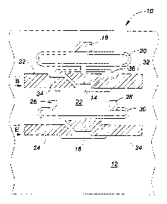
MEMS magnetically actuates switches shown in FIG. 2. FIG. l0A is a cross-
sectional
view of the MEMS switch through the A-A line and FIG 10B is a cross-sectional
view of
the MEMS switch through the B-B line. Referring to FIG. 10A, a microelectronic
16
CA 02328701 2000-12-15
Doc. No: CRO-37 CA Patent
substrate 200 has a thin dielectric layer 202 disposed thereon. The
microelectronic
substrate may comprise silicon, quartz, aluminum, glass or any other suitable
microelectronic substrate material. It is also possible to use a magnetic
material for the
substrate, such as ferrite nickel, if a non-magnetic dielectric layer is
disposed on the
substrate. The dielectric layer may comprise silicon nitride, silicon oxide or
any other
suitable dielectric material. The dielectric layer is typically disposed on
the substrate via
the use of conventional chemical vapor deposition (CVD) techniques. The
dielectric
layer serves to isolate the electrical load line conductor metals from the
substrate. The
second electrical load line 204 (the vertical load line in FIG. 2) is disposed
on the
substrate by standard patterning and etch procedures. The second electrical
load line may
comprise any conductive material, such as doped-silicon, copper, aluminum or
the like.
The dielectric tether device 206 is disposed within the material-free region
208 located
above the substrate. The material-free region is created by disposing
sacrificial layers
during processing that are subsequently removed to allow for certain
predetermined
structures to be free to move in prescribed directions. The dielectric tether
may be
formed of silicon nitride or any other suitable dielectric material may be
used. The first
electrical load line 210 (the horizontal load line in FIG. 2) is disposed on
the substrate
and above the tethering device. The first electrical load line may comprise
any
conductive material, such as copper, nickel, aluminum or the like. Typically,
the first
electrical load line will be overplated with a thin layer of metallic material
(not shown in
FIG. l0A), such as gold or the like, to insure low electrical resistance at
the point of
contact.
Refernng to FIG. lOB, similar to the FIG. l0A depiction the microelectronic
substrate 200 has a thin dielectric layer disposed thereon 202. Also, shown in
this
illustration, intermediate the substrate and the dielectric layer is a
clamping electrode
layer 212 that is disposed on the substrate. The clamping electrode layer in
the substrate
is used in unison with the magnetic element or an optional clamping electrode
224 to
create the clamping force. In certain embodiments in which the substrate is
conductive
the use of the buried clamping electrode in the substrate will not be
required. The
clamping electrode typically comprises a strong conductive material such as
copper or the
like. An anchor 214 is disposed on the substrate that serves to support the
tethering
17
CA 02328701 2000-12-15
Doc. No: CRO-37 CA Patent
device and provide clamping voltage to the clamping element. The anchor will
be
formed of a conductive material such as nickel or the like. A spring-like
element 216
will be affixed to the anchor and the magnetic element 218. The spring-like
element
provides a means for free movement of the tethering device and will typically
be formed
of a flexible, conductive material, such as polysilicon or a similar material.
The magnetic
element 218 will comprise a magnetic material, such as nickel, a nickel/iron
alloy or the
like. The dielectric tethering device 206 is disposed above and released from
the
microelectronic substrate. The tethering device serves as a platform for the
magnetic
element and the electrical element 220. The material-free region 222 below the
tethering
device is formed during fabrication by a sacrificial layer. The material-free-
region serves
to provide free movement to the tethering device. An optional clamping
electrode 224 is
disposed below and physically attached to the tethering device. The clamping
electrode
will typically comprise a strong conductive material, such as copper or the
like. In
embodiments in which the clamping electrode is disposed on the substrate, the
magnetic
element 218 and the clamping element may serve to provide electrostatic
clamping
capabilities; obviating the need to include the clamping electrode layer 212
in the
substrate. The electrical element 220 is disposed on the tethering device and
is typically
formed of a metallic conductor, such as nickel, gold, copper or alloys of the
same. The
electrical element is typically overplated with a low resistance material 226,
such as gold,
to insure proper electrical contact. A spring-like element 228 is attached to
the electrical
element and connects with the substrate and second electrical load line (not
shown in
FIG. lOB). The first electrical load line 210 is disposed on the
microelectronic substrate
in close proximity to the electrical element such that actuation of the
magnetic element
causes the connected electrical element to contact the first electrical load
line 210.
FIGS. 11A - 11E are cross-sectional views of various steps in the fabrication
of
the MEMS magnetically actuated switch in accordance with yet another
embodiment of
the present invention. Shown in FIG. 11A, is a microelectronic substrate 300
having a
ground clamp electrode layer 302 and a dielectric layer 304 disposed thereon.
The
microelectronic substrate may comprise silicon, quartz, aluminum, glass or any
other
suitable microelectronic substrate material. It is also possible to use a
magnetic material
for the substrate, such as ferrite nickel, if a non-magnetic dielectric layer
is disposed on
18
CA 02328701 2000-12-15
Doc. No: CRO-37 CA Patent
the substrate. The ground clamp electrode is typically formed from a metallic
material,
such as copper, nickel or the like, and is disposed by conventional diffusion
or deposition
techniques. FIG. 11B illustrates the MEMS magnetically actuated switch
construct after
a first conductive layer 306 has been deposited, patterned and etched to
define the second
electrical load line (i.e. the vertical load line in FIG. 2). The conductive
layer may
comprise a suitable conductive material, such as doped-silicon, copper or the
like.
FIG. 11C depicts the MEMS magnetically actuated switch after a first
sacrificial
layer 308 has been deposited, patterned and etch to define the areas where the
anchor will
connect with the substrate. The sacrificial layers will typically comprise a
low
temperature oxide material disposed by conventional LPCVD techniques and will
subsequently be removed to release predetermined elements from the substrate.
Shown in
FIG. 11D is the MEMS switch construct after a dielectric layer 310 has been
deposited,
patterned and etched to define the dielectric tether device. Typically the
dielectric layer
will comprise silicon nitride or another suitable non-magnetic dielectric
material may be
used. After deposition of the dielectric layer, a second sacrificial layer 312
is deposited,
patterned, and etched to define the areas on the tether device where the
magnetic and
electrical elements will be formed.
Referring to FIG. 11E, shown is the MEMS magnetically actuated switch after a
magnetic layer 314 has been deposited, patterned, and etched to define the
anchor
structures and the magnetic element. Typically, the magnetic layer will
comprise nickel,
nickel/iron alloy or a similar magnetic material. After the magnetic layer is
disposed and
defined, a second conductive layer (not shown in FIG. 11E) is deposited,
patterned and
etched to define the first electrical load line (i.e. the horizontal load line
in FIG. 2) and
the electrical element. The second conductive layer is typically formed from
copper,
nickel, aluminum or the like. After formation of the switch elements, a
release operation
removes the sacrificial layers to provide mobility to the tethering device.
As such, the present invention is capable of providing for a MEMS magnetically
actuated switch and corresponding switching arrays that are capable of
individual
activation in a single magnetic field environment. By implementing clamping
elements
the switches can be individually addressable in an array configuration. This
benefit can
be realized in easier fabrication of large scale switching arrays that occupy
less space on
19
CA 02328701 2000-12-15
Doc. No: CRO-37 CA Patent
the microelectronic substrate. Additionally, the present invention provides
for
embodiments that impart both in-plane and out-of-plane actuation.
Many modifications and other embodiments of the invention will come to mind to
one skilled in the art to which this invention pertains having the benefit of
the teachings
presented in the foregoing descriptions and the associated drawings.
Therefore, it is to be
understood that the invention is not to be limited to the specific embodiments
disclosed
and that modifications and other embodiments are intended to be included
within the
scope of the appended claims. Although specific terms are employed herein,
they are
used in a generic and descriptive sense only and not for purposes of
limitation.
20