Note: Descriptions are shown in the official language in which they were submitted.
CA 02329063 2000-10-19
WO 99/54842 PCT/NL99/00220
Substrate which is made from paper and is provided with an
integrated circuit
The invention relates to a substrate which is made
from paper and is provided with at least one integrated circuit.
A substrate of this nature is known from German Patent
Application DE-196 01 358, and is used in security documents and
banknotes to protect against forgery and fraud. This known
substrate comprises an integrated circuit which is incorporated
in the substrate and contains predetermined data. The IC is
contactlessly readable and is joined to the substrate in a non-
releasable manner. The IC which is used in this substrate is a
conventional IC, i.e. of the well-known silicon type. The
dimensions of the chip originally produced are reduced by means
of etching or polishing, so that the chip acquires the thickness
which is desired for it to be incorporated in the paper mass. In
order to prevent damage to the crystalline circuits, the IC is
reinforced with the aid of a support layer, which also serves to
position the IC. Furthermore, the IC is covered with a protec-
tive, chemically resistant layer. The lack of flexibility of
this known silicon chip is a drawback when a substrate of this
nature is used as a security paper, for example in banknotes and
identity documents. In addition, the extra layers which are to
be included, as well as the additional processing step for
producing the appropriate dimensions, lead to an additional
increase in the cost price of a substrate of this nature.
The object of the present invention is to provide a
paper-based substrate for use in security documents, banknotes
and the like, in which an integrated circuit is incorporated,
which substrate does not have the drawbacks mentioned above.
According to the present invention, this object is
achieved with a substrate of the type mentioned above in which
the integrated circuit comprises a semiconductive organic
polymer. This means an electronic circuit which is arranged in
the polymer material and the contents of which are programmed in
order to assign it a specific function. Polymer chips of this
nature are highly flexible and are therefore eminently suitable
for use in security documents such as banknotes. Even sharp
creases in the chip made from a semiconductive organic polymer
CA 02329063 2006-01-20
- 2 -
do not impede the functioning of the chip. In addition,
poly-meric ICs can be produced directly in the desired
dimensions, in particular with regard to thickness, and
the costs of a chip of this nature are lower by
approximately a factor of 10 than the current lowest price
for a chip of the silicon type.
In the polymeric chip, the nonconductive support
on which the semiconductive polymer material is deposited
substantially determines the thickness of the overall
integrated circuit. It is preferable to use a
mechanically strong insulator: plastics with strong
intramolecular and intermolecular interactions are
particularly suitable for this purpose.
Using an IC of this nature as a security mark in
security paper and similar items provides novel and
powerful means of protection, since producing these ICs is
much too complicated for forgers and generally far exceeds
their knowledge and capabilities.
In the context of this application, paper is
understood to mean paper which is made from natural or
synthetic fibres, as well as "paper" which can nowadays be
produced from plastic films, which paper is used for the
production of security paper, banknotes and the like.
Furthermore in the context of this application
the term "substrate" denotes the papermass in which the IC
is embedded or upon which IC is applied. The term "non
conductive support" denotes the device on which the active
layers of the IC are formed, which device is in the field
of IC's commonly denoted as substrate.
The integrated circuits may number one or more
and may be adjusted as a function of the requirements. For
example, with a view to certainty of operation, it is
possible to incorporate two or more identical polymer
chips, so that in the event of one of these chips failing
CA 02329063 2006-01-20
- 2a -
the substrate and/or the end product which has been
produced therefrom can still be used.
Preferably, the organic polymer is selected from
conjugated polymers, in particular from oligomeric
pentacene, poly(thienylene vinylene) or poly-3
alkylthiophene. An IC which is produced from one of these
materials is described by Brown et al. in Science, 270,
pp. 972 - 974, 1995.
As will be understood by the skilled person, the
plastic IC, used in the invention, comprises additional
layers of different polymers besides the semiconductive
polymer layer. For example, the substrate may be produced
from polyimide, on which polyaniline blocks are formed,
which function as source and drain. On top thereof, the
semiconductive polymer layer is present, e.g. comprising
poly(thienylene vinylene). This layer is covered by an
insulating layer, e.g. from polyvinylphenol,
CA 02329063 2000-10-19
WO 99/54842 - 3 _ PCT/NL99/00220
while a top layer of polyaniline is the uppermost layer, which
is the gate.
In an embodiment of the substrate according to the
invention, the integrated circuit is contactlessly readable, the
data transmission being brought about: by an inductive or
capacitive route, as is known in the prior art.
In case of inductive readout a coil is needed for the
current supply, which has to be connected conductively to the
IC; thereby making possible readout from a distance. In order to
be able to readout at a small distance it is necessary that the
IC contacts a conductor, wherein this conductor together with
the measuring apparatus creates a capacity, whereby the current
supply and readout become possible.
According to another preferred embodiment of the
substrate according to the invention, the substrate comprises a
conductive security thread which is connected to the integrated
circuit, which security thread serves as a direct contact or
indirect contact for the readout and for supplying the current.
In a preferred embodiment thereof, the security thread is
metallized in order to provide the required electrical conduc-
tivity, except at the position of the polymeric IC, where the
deposition of metal is interrupted. In the case of direct
current supply the metal has to be accessible. Possible ways of
providing this accessibility comprise a security thread which is
incorporated in the substrate, as well as a security thread
which is incorporated in the substrate and the metal parts of
which are accessible via so-called windows. Advantageously, one
or more integrated circuits are part of the security thread
itself. The thickness of this security thread may be adapted to
the intended use of the substrate, for example in banknotes. For
banknote paper, the thickness of the paper substrate usually
lies in the range up to 100 m. In this case, the thickness of
the security thread preferably lies in the range of 15-60 s of
the thickness of this substrate. If the paper substrate has a
different thickness, as for example for a cover of an identity
document such as a passport, a minimum thickness of the security
thread of approximately 10 m applies. A thickness greater than
100 m is relatively meaningless for use in security paper. The
preferred embodiment of a polymeric IC in the form of a security
thread provides an additional security feature which can easily
CA 02329063 2000-10-19
WO 99/54842 PCT/NL99/00220
- 4 -
be recognized by the public. The thread comprising an integrated
circuit may additionally comprise a number of other features,
such as a dye, fluorescent or phosphorescent material, lumines-
cent material and printed indices.
Organic, conductive polymers can also be used for
supplying the current to the chip, although in case of direct
contact the mechanical contact properties of these polymers cur-
rently still leave something to be desired.
A simple security thread which consists of conductive
polymers is proposed in European Patent Application
EP-A-0,753,623. However, a thread of this nature has only
conductive properties. There are no semiconductor properties,
and therefore it is not possible to apply and store a code in a
manner which is comparable to a conductive polymer thread in
which an integrated circuit is incorporated. The security thread
comprising an integrated circuit according to the invention can
be arranged in the customary way, for example by being incorpor-
ated completely or integrated in the paper mass, in a window or
by being attached to the surface of a document. If protection
against attack from chemicals is required, a chemically resis-
tant, electrically nonconductive protective layer may be applied
to the conductive organic polymers of the chip.
The polymeric chip does not per se have to be com-
pletely incorporated in the paper, as is the case for the
silicon chip in the German patent application mentioned above.
As an alternative, the polymeric IC may also be arranged on the
surface of the substrate, using customary techniques for attach-
ing foils, holograms, other optically active elements and the
like.
The integrated circuit may also advantageously itself
form part of all sorts of optically active elements, such as
foils, patches, holograms or kinegrams, which are arranged on or
in the substrate as additional security features. As has already
been described above with regard to a security thread, according
to a further preferred embodiment it is also possible to shape
optically active elements of this nature in such a manner that
two electrically separate conductive parts of such elements
function for readout and current supply, both directly and
capacitively. The conductive parts may consist of metal, conduc-
tive polymer or a combination thereof.
CA 02329063 2000-10-19
WO 99/54842 - 5 - PCT/NL99/00220
For protection purposes, the integrated circuit may
comprise a preprogrammed code, which code is applied before the
chip is incorporated in the substrate.
Advantageously, the integrated circuit comprises a
code of an intrinsic property of the substrate in which the
circuit is incorporated.
In the current state of the art, the polymer IC may be
used only in one direction; i.e. it can be written or programmed
once. A preferred way of storing a code in the IC is to use
techniques which are derived from cryptology. The authentic code
is then stored in the IC in an encrypted manner, and deciphering
is impossible without knowing the secret key. Thus, even if
unwritten chips could be obtained illegally, the secret key
forms a powerful and virtually impregnable barrier preventing
the forger from applying a message to security documents and
reading this message out. The protection can be improved still
further if the optionally partial programming of the chip is
carried out after the IC has become part of the security docu-
ment, as will be explained in more detail below.
The shape of the polymer chip is not critical. Cur-
rently, a dimension of approximately 1. mm for a rectangular
shape represents the lower limit of a surface dimension if a
reasonable number of bits are to be stored in the IC. A rec-
tangular IC of 4 mm by 6 mm currently holds approximately 48
bits, i.e. two bits/mm2. The ratio of the surface dimensions for
a polymer chip (i.e. length to width) should preferably not
exceed 10:1, owing to the resultant undesirable build-up of the
chip given larger ratios. The small dimensions of an IC offer
the possibility of covering the chip with additional features
which are customarily used in the prior art. The dimensions of
such additional features are generally large compared to the
dimensions of the polymeric IC. Thus even large ICs, with
sufficient memory capacity for storing large quantities of data,
can be used without impairing the appearance of the security
paper. If a combination of a chip with another security mark is
arranged on the security paper, it is necessary to ensure that
reading and supplying current to the chip are not adversely
affected by an additional security feature of this nature.
The substrate comprising a polymer IC according to the
invention is used as a security paper in, for example, bank-
CA 02329063 2000-10-19
WO 99/54842 - 6 - PCT/NL99/00220
notes, passports, identity cards and other security documents,
such as securities.
The development of an inexpensive integrated circuit
of this nature offers a number of novel possibilities for
preventing forgery of security documents, beginning with a
completely new type of electronics (electronic bar codes) in
security paper.
Examples of the use of an IC as a security feature in
a document which will be described are the various possibilities
for a banknote, but comparable possibilities likewise exist for
other types of security documents, such as passports, identity
cards and the like.
A first possibility relates to the use of a completely
preprogrammed IC in the substrate made from paper. The IC
contains one or more codes, if desirable in encrypted form,
relating to the banknote. This information may comprise the
value, the country, the place and/or time of production, number
and the like. For a specific value of the banknote, the informa-
tion on each chip is substantially identical, i.e. value,
country and usually the paper manufacturer and/or printer, and
partially different, i.e. production time, production numbers
and sometimes paper manufacturer and/or printer.
A more specific protection is obtained with a chip
which is partially preprogrammed with a unique code (first code)
and an additional second code. This second code is an encrypted
translation of the first code. Encryption is carried out using a
first key. In the event of verification, the second code is read
and the encrypted relationship to the first code is verified
using a second key. The second code can be applied to the chip
before or after the chip has been arranged in the substrate. An
encryption system of this nature is described, by way of
example, in WO-A-97/24699.
In this known system, an intrinsic property of the
object is coded, encrypted and enciphered. For banknotes,
surface properties are taken at a special location, coded,
encrypted and stored as a printed pattern on the banknote. In
the event of verification, the printed pattern and the surface
property are compared with one another using a second key.
Many other properties, as well as properties distrib-
uted arbitrarily in the substrate, are used in the prior art for
CA 02329063 2000-10-19
WO 99/54842 PCT/NL99/00220
- 7 -
the protection of security documents, cf., inter alia,
WO-A-91/19614 (fibre direction), GB-A-230,407 (reflective
flakes), US-A-4,218,764 (magnetic particles or fibres) and
WO-A-87/01845 (conductive fibres) . In all these cases, arbitrary
and therefore unique properties of a document are used for the
verification. Hitherto, there has been no suitable chip avail-
able for use in paper substrates in order to store the
(encrypted) code, and consequently a coded property was always
stored in another way, for example outside the document itself,
or was printed in or on the document or recorded magnetically
therein. The polymeric chip which is used in the substrate
according to the invention makes it technically possible to use
and store these protection features inside the document.
The fluorescence properties of arbitrarily distributed
fluorescent fibres in a predetermined area of the banknote may
be a suitable property. However, any other property which can be
measured and is arbitrarily distributed in or on the paper may
also be used. A condition is that the property used must be
stable throughout the entire lifespan of the document, which
means that any property which is highly dependent on the conse-
quences of use, such as soiling, contamination, creasing and the
like, is in principle unsuitable.
The coordinates of the relevant part of the banknote
where the arbitrary property is determined and, if necessary,
the orientation in which the surface must be examined may also
be stored in the chip. Thus, when verifying the banknote, a
specific parameter is measured along a predetermined path, or an
image of the entire banknote is taken, but the assessment is
carried out using only the data found at the precoded
coordinates. The result of this measurement is compared with the
stored code, which likewise refers to the same property at the
same location. On the basis of this comparison, which may
optionally be encrypted, a rejection or acceptance signal is
generated.
The substrate with a polymeric IC according to the
invention may furthermore comprise customary security features,
such as watermarks, security threads, optically active elements
and special chemicals, microprints, etc., standard techniques
being used to determine these features.
The invention also relates to a security thread or
CA 02329063 2000-10-19
WO 99/54842 - 8 - PCT/NL99/00220
optically active element comprising an integrated circuit made
from a semiconductive organic polymer.
The following example illustrates the invention. In
this case, specific fluorescent properties in a specific part of
the document are used as an example. Many banknotes are supplied
with a number of highly fluorescent fibres which emit different
colours of light. These fibres are distributed arbitrarily
through the document. The local fluorescence of various types of
fibres at a predetermined location can be coded and digitally
stored in the chip, optionally in encrypted form, at the time
the document is produced, i.e. during the paper manufacturing
phase or during the document printing phase. In the event of
verification, the area in question is read again using the
coordinates and orientation which are stored in the chip, and
the results are compared with one another, followed by rejection
or acceptance. The said coordinates and orientation will gen-
erally differ for each separate banknote, with the result that
verification is completely unique for the said document, since
the arbitrary property and coordinates are unique for that
document. In this way, the chip of each separate banknote
contains a unique code which, as it were, represents a finger-
print of a specific part of the banknote in question. The code
of the intrinsic property may be stored either in encrypted or
nonencrypted form.
As has already been mentioned above, the use of the
substrate according to the invention is not limited to bank-
notes. For other uses, such as passports and identity documents,
part of a biometric property of the legal owner can be used to
generate a digital code which is then stored in the IC of the
document. One such example could be a coded part of a digitized
photograph of the legal owner, the part to be digitized being
determined by coded parameters which are unique for each docu-
ment. Entirely as for the example given above, verification of
the document requires the stored code of the photograph and the
code actually read to match one another. Other biometric parame-
ters may also be used, such as fingerprints or parts thereof,
which are then stored in coded form in the polymer chip. Here
too, it is necessary for the coded, stored feature to be stable.
To illustrate the invention further, reference is made
to the appended drawing, in which:
CA 02329063 2000-10-19
WO 99/54842 - 9 - PCT/NL99/00220
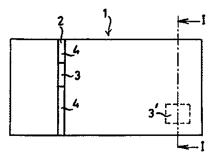
Fig. .1 shows a diagrammatic plan view of an embodiment
of a banknote according to the invention;
Fig. 2 shows a cross section through the banknote
illustrated in Fig. 1, along line I-I;
Fig. 3 shows a diagrammatic plan view of another
embodiment of a banknote according to the invention;
Fig. 4 shows an enlarged illustration of an optically
active element which is used in the banknote in accordance with
Fig. 3;
Fig. 5 shows a cross section through the optically
active element illustrated in Fig. 4;
Fig. 6 shows a cross section through yet another
embodiment of a banknote according to the invention;
Fig. 7 shows a further embodiment of a security thread
with polymeric chip;
Fig. 8 shows another embodiment of an optically active
element with polymeric chip;
Fig. 9 shows a combination of =a security thread and
optically active element; and
Fig. 10 shows yet another embodiment of a security
thread according to the invention, in cross section.
It should be noted that, in the figures which are to
be discussed below, identical components are denoted by ident-
ical reference numerals.
Fig. 1 shows a banknote 1 made from paper. The bank-
note 1 comprises a security thread 2 containing a chip 3 made
from a semiconductive organic polymer and conductive e.g.
metallized parts 4. Furthermore, the banknote 1 comprises a
second chip 3', which is likewise made from a semiconductive
organic polymer. As can be seen from the cross section in
accordance with Fig. 2, the security thread 2 is arranged on the
paper 5, while the second polymeric chip 3' is embedded in the
paper mass 5. The embedded chip 3' makes contact with a
conductor or coil so as to provide the current required and
readout.
Fig. 3 shows another embodiment of a banknote 1, in
which the security thread 2, which again contains a polymeric
chip and conductive parts 4, is incorporated in the paper mass.
Sections of the conductive parts 4 are accessible via windows 6
in order to make direct electrical contact, if desired. The
CA 02329063 2000-10-19
WO 99/54842 - 10 - PCT/NL99/00220
banknote 1 illustrated in Fig. 3 also comprises a second chip
3', which in this case is situated beneath an optically active
element 7. The optically active element 7 comprises conductive
parts 8 which are separated by a strip 9 which is insulating,
i.e. nonconductive. The chip 3' can be read and supplied with
power via the conductive parts 8, whether directly or from a
distance via capacitive coupling. The conductive part may be
covered by a chemically inert layer, if readout is done
capacitively. If direct contact is required, a part of the
conductor and the entire part 9 can be covered in such a way
that the IC and conductor are protected (with a nonconducting
material), while other parts of the conductor are still acces-
sible to direct contact.
Fig. 4 shows an enlarged view of the optical element 7
with chip 3', while Fig. 5 is a cross section through an optical
element 7 of this nature.
Fig. 6 shows a further embodiment of a security thread
2 with a chip made from semiconductive organic polymer 3 and
conductive parts 4, which is applied on the paper 5. In this
embodiment, the polymer chip and sections of the conductive
parts 4 of the security thread 2 are protected by means of a
layer 10 of a chemically resistant, electrically nonconductive
material. The protecting layer 10 may cover the entire thread,
if capacitive coupling is used.
Fig. 7 shows yet another embodiment of a security
thread according to the invention, in which the chip 3 does not
form part of the security thread itself, but rather is posi-
tioned next to it. The conductive parts 4 of the security thread
2 are electrically insulated from one another by means of
insulator block 4. The chip 3 is connected to the relevant
conductive parts 4 of the security thread via electrical conduc-
tors 12.
An embodiment of the same type for an optically active
element is illustrated in Fig. 8. The electrical conductors 12
provide the electrical contact between the conductive parts 8 of
the optically active element and the polymeric chip 3'.
Fig. 9 shows a combination of a security thread 2 with
optically active element 7, the metal parts 4 of the security
thread 2 making electrical contact with the metal parts 8 of the
optically active element 7. A chip made from semiconductive
CA 02329063 2000-10-19
WO 99/54842 PCT/NL99/00220
- 11 -
organic material 3' is situated beneath the optically active
element 7.
Fig. 10 illustrates yet another embodiment of a
security thread according to the invention. In this embodiment,
the security thread is composed of a chip 3 and conductive parts
13, which are made from a conductive polymer. The security
thread is arranged on the paper 5. The polymer chip 3 is pro-
tected with a layer 10 of chemically resistant material, which
also covers (sections of) the conductive polymer 13. In order to
ensure a very good supply of power and readout, metal blocks 14
are arranged next to the layer 10 of insulating material, which
metal blocks 14 are electrically connected to the conductive
organic polymers 13.
In case of a system using capacitive coupling an additional
protecting layer may be applied over the metal parts 14 and the
chemically resistant layer 10.