Note: Descriptions are shown in the official language in which they were submitted.
CA 02329334 2002-12-17
WO 99/43058 PCTILiS99103534
-~l
FIBER OPTIC LASERS EMPLOYING FIBER OPTIC AMPLIFIERS
Cross-Reference to Related A~lications
This Application claims priority to L~.S. Provisional Application No.
60/07,339, filed February 20, 1998, Attorney Docket No. 0953.048. entitled
''SIDE POLISHED FIBER-OVERLAY LASERS".
This Application relates to the following previously filed, commonly
assigned, U.S. Patent Applications:
U.S. Patent Application No. 08/786,047, filed January 21, 1997,
Attorney Docket No. 0953.023, now U.S. Patent No. x.81 x,309
issued September 29, 1998, entitled, "OPTICAL AMPLIFIER AND
PROCESS FOR AMPLIFYING AN OPTICAL SI<iN AL
PROPAGATING IN A FIBER OPTIC;"
1 s U.S. Patent Application No. 08/928,578, filed September 12, 1997.
Attorney Docket No. 0953.023A, now U.S. Patent No. 6,052,220, entitled,
"OPTICAL AMPLIFIER AND PROCESS FOR AMPLIFYING AN
OPTICAL SIGNAL PROPAGATING IN A FIBER OPTIC EMPLOYING AN
OVERLAY WAVEGUIDE AND STIMULATED EMISSION;"
U.S. Patent Application No. 08/786,033, filed January 21, 1997, Attorney
Docket No. 0953.021, now U.S. Patent No. 5,892,857, entitled "ELECTRO-
OPTIC COMPOUND WAVEGUCDE MODULATOR;" and
U.S. Patent Application No. 08/785,871, filed January 21, 1997, Attorney
CA 02329334 2002-12-17
WO 99/43058 PCT/US99/0353
,._7 _
Docket No. 0953.022, now U.S. Patent No. 6,026,205, entitled "COMPOUND
OPTICAL WAVEGUIDE AND FILTER APPLICATIONS THEREOF."
Technical Field
The present invention relates to fiber optic ring and linear caviy lasers
formed using optical amplifiers, which employ stimulated emission or optical
parametric amplification, in compound waveguide conFgurations.
Back ;round of the Invention
The present invention is intended to provide a laser source for any
wavelength, and of the type already known using erbium-doped fibers at 1~~0
nnl.
Current in-line fiber optic amplifiers operate in the 1300 nm
telecommunications window utilizing Neodymium (Nd)-doped gain media (both
glasses and YAG). These devices provide single-pass gain to compensate for
1 ~ propagation losses incurred in optical fibers. A laser is the extension of
single-pass
amplification to multiple-pass oscillation by the addition of a cavity. In
most
conventional laser systems, the cavity is created using two or more mirrors.
While
a plethora of lasers have been developed using mirror cavities, extending
these
systems to fibers requires the use of costly and delicate fiber-coupling
systems.
Some fiber laser systems have been developed in which a section of ion-
doped fiber is splice:? into a fiber ring, which acts as the cavity.
Unfortunately, only
a handful of doped glasses have been developed which can be fashioned into
optical fibers, which provide only very sparse coverage of the entire optical
spectrum.
CA 02329334 2000-10-19
WO 99/43058 PCT/US99/03534
-3-
What is required, are improved laser systems employing advanced optical
amplification technology.
The present invention provides a compound waveguide architecture and
associated amplification tf:chniques to address this need, in both ring and
linear
cavity laser system configurations.
Summary of the Invention
The present invention, in one aspect, is a laser system including a fiber
optic amplifier arranged with respect to an interior portion of a fiber optic
having a
side surface through which. optical energy can be transferred to or from the
fiber
1'D optic. The fiber optic amplifier includes a channel overlay waveguide
formed over
the surface for amplifying '.the optical energy therein for transfer to an
optical signal
propagating in the fiber opvtic. The fiber optic is arranged into a cavity, an
output
of which comprises laser energy generated within the cavity using the
amplified
optical signal propagating in the fiber optic. The cavity may be ring or
linear, and
15 the system may include various intracavity elements for, e.g., wavelength
selection,
optical isolation and modu',lation of the optical signal propagating in the
fiber optic.
Two alternative amplification technologies are disclosed, including
stimulated emission which uses channel overlay waveguides exhibiting optical
fluorescence. Optical parametric amplification can also be used, in which case
the
2~~ channel overlay waveguide; exhibits a non-linear response of second order.
Associated methods of producing laser energy, as well as methods for
fabrication
of a laser system are also disclosed.
In summary, disclosed herein are fiber optic laser systems employing
alternate embodiments of an in-line, non-invasive fiber optic amplifier. The
lasers
2.5 of the present invention err~ploy these fiber optic amplifiers in either
fiber ring or
linear cavity configurations. The flexibility of the non-invasive fiber optic
amplifier
CA 02329334 2000-10-19
WO 99/43058 PCT/US99/03534
-4-
technology allows these laser systems to be designed and constructed for both
narrowband and broadban<1 operation. As such, either the amplifier itself, or
a
separate component, can act as the wavelength determining element in the
cavity.
These lasers provide a stable, fiber coupled source that can be used with
nearly any
S gain material to produce fiber coupled laser energy at an enormous variety
of
wavelengths. Such wide wavelength coverage will benefit medical imaging,
communications, remote sensing, and other scientific research.
Brief Description of the Drawings
The subject matter which is regarded as the invention is particularly pointed
out and distinctly claimed :in the concluding portion of the specification.
The
invention, however, both as to organization and method of practice, together
with
further objects and advantaiges thereof, may best be understood by reference
to the
following detailed description of the preferred embodiments) and the
accompanying drawings in which:
Figs. la & 1b are cross-sectional views of a polished fiber/overlay
compound waveguide in accordance with one aspect of the present invention,
Fig.
1b being taken along line l b-lb of Fig. la, and Fig. la being a cross-
sectional
view taken along line 1 a-1 a of Fig. 1 b;
Fig. 1e comprises a~ perspective view of the compound waveguide depicted
in Figs. la & 1b;
Figs. 2a-2c comprise alternative embodiments of a channel overlay
waveguide for a compound waveguide in accordance with the present invention;
Fig. 3 is a plot of power intensity in the fiber optic compared with
wavelength for a conventional "slab" overlay waveguide compared with a channel
overlay waveguide in accordance with the present invention;
CA 02329334 2000-10-19
WO 99/43058 PCT/US99/03534
-5-
Fig. 4 is a plot of optical power intensity in a fiber optic compared with
interaction length, again for a conventional "slab" overlay waveguide
contrasted
with a channel overlay waveguide in accordance with the present invention;
Figs. 5a & 5b comprise cross-sectional views of multiple embodiments of
an optical amplifier in accordance with the present invention, Fig. 5a
comprising a
cross-sectional view taken along line Sa-Sa of Fig. 5b, and Fig. 5b comprising
a
cross-sectional view of the optical amplifier taken along line Sb-Sb of shown
in
Fig. 5a;
Fig. 5c is a plot of experimentally observed gain spectrum for a side-
1 D polished fiber amplifier with a Nd:YAG crystal used as the overlay
waveguide,
with the waveguide pumped with 700 mW of light at 808 nn;
Fig. 6 is a plot of amplifier gain versus interaction length for a lithium
niobate based device;
Fig. 7 is a plot of amplifier gain versus pump power for a lithium niobate
15 based device;
Fig. 8 is a plot of normalized dispersion-limited gain bandwidth for a
lithium niobate based device;
Fig. 9 is a graphical representation of optical parametric amplification
employing a seed signal comprising optical energy transferred to the channel
2n overlay waveguide from the fiber optic pursuant to the present invention;
Fig. 10 is a representation of prism coupling in accordance with the present
invention;
Fig. 11 depicts examples of mis-matched and matched modes useful in
CA 02329334 2000-10-19
WO 99/43058 PCT/US99/03534
-6-
describing mode matching in accordance with the present invention;
Fig. 12 is a cross-sectional view of an alternate embodiment of an optical
amplifier in accordance with the present invention, wherein a low index
matching
layer is disposed between the coupling surface of the channel overlay
waveguide
:> and the fiber optic;
Figs. 13a & 13b depict amplifier performance for a lithium niobate device
at wavelength 1310 nm in accordance with the present invention, Fig. 13a
depicting device gain versus interaction length, and Fig. 13b plots device
gain
versus input or pump power applied to the amplifier;
Fig. 14 is a cross-sectional view of an alternate embodiment of an optical
coupler in accordance with the present invention having bandwidth enhancement;
Fig. 15 depicts a first embodiment of the laser system of the present
invention employing a ring cavity; and
Fig. 16 depicts a second embodiment of the laser system of the present
1.'i invention employing a linear cavity.
Detailed Description of the Invention
As discussed above., the present invention is directed to laser systems
employing advanced ampli:&cation technology. Discussed first is the enabling
amplification technology with respect to Figs. 1-14, followed by a disclosure
of the
laser systems 1000, 1100 of the present invention with respect to Figs. 15-16.
Amplification Technology:
As noted, the present invention employs a polished fiber/overlay compound
CA 02329334 2000-10-19
WO 99/43058 PCT/US99/03534
waveguide architecture which implements an optical amplification method for
fiber
optic systems. The compound waveguide efficiently amplifies small signals
that,
e.g., have been attenuated .due to long distance transmission. The
amplification is
carried out by the process o~f stimulated emission, or by type I optical
parametric
:> amplification. Advantageously, as an all-optical signal amplifier, there is
no
discontinuity created in the optical fiber network, aiding in minimization of
losses
and instabilities.
As noted, the present technique involves ane of two amplification methods.
The first employs stimulated emission, whereby a material with strong
fluorescence
characteristics is pumped by a high-power laser diode. For example, neodymium-
doped (Nd) yttrium aluminum garnet (YAG) (Nd:YAG) materials can be used as
an overlay waveguide and pumped with an 808 nm 1 watt laser diode source. Any
process able material can be used in this architecture which means any
material that
fluoresces can be utilized as an amplifier. In fact, members of the Neodymium
1.'. family of glasses that were previously thought to be inefficient can be
used. This is
because the absence of a finer discontinuity in a structure pursuant to the
present
invention prohibits the forniation of a cavity, and minimizes the possibility
of
lacing at 1064 nm. Furthen:nore, because the material need not be drawn into a
fiber, the subset of usable materials expands dramatically to include glasses
and
2(I crystals in which excited st<~te absorption is not a problem. Thus, in
accordance
with the principles of the present invention, the constraints on the process
are
solely the concentration of :fluorescent atoms or ions, the stimulated
emission
cross-section, and the availability of high-power pump sources. Given that
lasers
have existed for 30 years arid given recent strides in the field of high-power
laser
2'. diodes, none of these constraints are significant barriers to successful
implementation of this invention.
The second amplification method involves the use of second-order
nonlinear frequency conversion to down-convert a high-power, short-wavelength
pump to amplify an optical signal propagating in a fiber optic. Parametric
CA 02329334 2000-10-19
WO 99/43058 PCT/US99/03534
_g_
amplification is limited onily by device length and material non-linearities.
With
the compound architecture presented, existing materials can provide gain
comparable to that provided by conventional erbium-doped fiber amplifiers, but
at
any wavelength desired provided a pump source exists. This is hardly a
limitation,
however, based on the versatility of current high-power diode laser
technology.
The optical amplifier and amplification process in accordance with this
invention employs a polished fiber/overlay compound waveguide architecture
such
as disclosed in detail in the above-referenced, commonly assigned U.S. patent
applications directed to the related filter and modulator structures. This
compound
architecture is briefly discussed below.
As is known, an optical waveguide can be a useful device for selective
coupling of a specific optical signal from a portion of a broad-band fiber
optic
placed in optical proximity thereto. When a single-mode optical fiber, side-
polished close to the core, is placed in proximity to a high index, "overlay"
1:> waveguide, the compound .device's spectral response is that of a periodic
bandstop
wavelength filter. In this configuration, the waveguide is positioned in
optical
proximity to the fiber such that coupling occurs within the "evanescent" field
of the
optical signal transmitted within the fiber, resulting in a non-invasive
coupler
which does not suffer insertion losses associated with in-line couplers which
21) interrupt the fiber core itself
Refer now to the drawing figures wherein the same reference numerals are
used throughout multiple figures to designate the same or similar components.
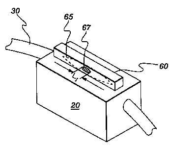
Figs. la-lc depict an exemplary side-polished optical fiber/channel overlay
compound waveguide, generally denoted 10, in accordance with the present
2:i invention. Compound waveguide 10 includes a substrate 20 having a first
waveguide 30 running therethrough. Waveguide 30 comprises, for example, an
optical fiber having a core ~40 encased by cladding 50. The fiber transmits an
optical signal through its core along propagation axis a~. Assuming that
optical
CA 02329334 2000-10-19
WO 99/43058 PCT/US99/03534
-9-
fiber 30 comprises a single-mode optical fiber side-polished close to its
core,
optical coupling is possible; to an overlay waveguide 60. The compound
waveguide spectral response is that of a periodic bandstop wavelength filter.
In accordance with the invention, overlay waveguide 60 comprises a
:> "channel" overlay waveguide which as discussed further below constrains
optical
energy within a predefined area orthogonal to the propagation axis of the
optical
energy within the channel overlay waveguide. The predefined area constrains
the
optical energy to the vicinity of the fiber optic. C>verlay waveguide 60
optically
couples the evanescent field exposed by the side-polishing of fiber optic 30.
This
evanescent coupling occur:. at least over an optical interaction area 67
(having
interaction length L,) betwf:en channel waveguide 60 and fiber waveguide 30,
which in exemplary device embodiment 10 is substantially determined by the
size
of the intersection 65 of the; planar polished surface of fiber waveguide 30
and the
lower, coupling surface of channel waveguide 60. Interaction length L, is
typically
l :p much smaller than the length of the channel waveguide. As discussed
further
below, although Figs. la-lc depict direct contact between fiber optic 30 and
overlay waveguide 60, an intervening adhesive and/or index matching layer may
be
present at this coupling intc;rface.
Evanescent coupling occurs between fiber optic 30 and waveguide 60 in the
exposed evanescent field wea of the optical signal transmitted along axis a,
of fiber
optic 30. This evanescent coupling causes optical energy to be transferred to
the
channel overlay waveguide: from the optical signal propagating in fiber optic
30.
Channel overlay waveguide 60 confines diffraction of coupled optical energy to
a
predefined area transverse, or orthogonal, to the axis of propagation of the
optical
energy within the overlay. This predefined area is in the vicinity of the
fiber optic
such that all coupled optical energy remains in the overlay substantially
directly
over the fiber optic and is therefore available for coupling back into the
fiber optic
subsequent to being amplified in accordance with the invention. Axis a, and
axis
a3 are depicted in Fig 1b as, two exemplary axes orthogonal to the direction
of
CA 02329334 2000-10-19
WO 99/43058 PCTNS99/03534
-10-
propagation of optical energy within the channel overlay waveguide 60. Again,
transfer or lateral diffraction of coupled optical energy within the overlay
waveguide is constrained by the optical boundaries of the waveguide 60, which
may be defined by the physical shape of the waveguide as explained further
below.
Further, pursuant to the present invention, this confinement of optical energy
within the overlay waveguide is substantially directly over the fiber optic
such that
the optical energy coupled from the optical signal propagating in the fiber
optic
remains in the vicinity of the fiber optic for subsequent coupling back into
the fiber
optic along the length L, of the compound waveguide.
Figs. 2a-2e depict various configurations of a channel overlay waveguide
for use in accordance with the present invention. Each of these waveguides
effects
confinement of coupled optical energy to a defined area in a directional
transverse
or orthogonal to the axis of propagation of the optical energy within the
waveguide.
In Fig. 2a, compowld waveguide 110 includes layer I70 which is
l :i substantially planar. Layer 170 is deposited over substrate 20 containing
the side-
polished optical fiber including core 40 and clad 50. Layer 170 includes a
channel
waveguide 160 defined by a material with index of refraction no which is
greater
than the indices of refractia~n of the material n on either side. Optical
boundaries
162 and 164 at these regions of differing indices serve as the optical
boundaries
21) which confine optical enerl;y within waveguide 160 transverse to an axis
of
propagation of the energy within the waveguide. As with boundaries 162 and
164,
upper boundary 166 confines the optical energy along the vertical axis.
Various
fabrication techniques can be employed to realize the structure of Fig. 2a.
Fig. 2b presents a compound waveguide architecture 210 which similarly
2:i includes a layer 270 deposited over substrate 20 having a fiber optic
embedded
therein comprising core 40 and cladding 50. A channel waveguide 260 is formed
by doping (e.g., via ion implantation) layer 270 in the vicinity of the fiber
optic
such that the channel wave;guide 260 is disposed over core 40 of the fiber
optic.
CA 02329334 2002-12-17
WO 99/43058 PCTIUS99/03534
Waveguide 260 has an index of refraction n~ which is greater than the index of
refraction n of the remaining portions of layer 270 such that optical
boundaries 262
and 264 are formed on either side of waveguide 260. These boundaries. in
addition
to an upper boundary 266 Serve to confine optical energy coupled into the
overlay
waveguide within channel 260 for subsequent return to the fiber optic.
As another alternative, a compound waveguide architecture 310 is depicted
in Fig. 2c wherein a channel waveguide 360 is realized using a relief
structure 366
on the upper surface of layer 370 disposed over substrate 20 within which the
'optical fiber resides. Optical boundaries 362 and 364 can be realized using
such a
relief structure. These boundaries define a cross-sectional area disposed
orthogonal
to the axis of propagation of optical energy within channel 360. One method of
creating such a relief structure is disclosed in commonly assigned U.S. Patent
x,396,362 entitled "High Resolution MicroMachining of Organic Crystals and
Optical Modulators Formed Thereby," issued March 7, 1996.
The above-described channel waveguide presents improved optical
characteristics compared with those of standard planar or "slab" waveguides as
evidenced by the spectral response plot of Fig. 3. This figure comprises a
comparison of the periodic bandstop characteristic 420 of a channel wave~uide
superimposed over the periodic bandstop characteristic 410 of a planar or slab
waveguide. These characteristics are for the optical signal propagating in
fiber 30
following its interaction with channel 60. As shown, spectral characteristic
420
has a "sharper" response resulting in smaller transition regions in the
bandstop
areas than those of spectral characteristics 410. The difference in the
spectral
2~ responses is represented as hashed region 430, which depicts the improved
characteristic of the channel waveguide over a planar or slab waveguide. This
spectral response is due in large pan to minimization of lateral diffractive
losses
provided by the channel overlay waveguide.
CA 02329334 2000-10-19
WO 99/43058 PCT/US99/03534
-12-
The present invention is based on a recognition that the absence of lateral
diffractive losses in a chanmel waveguide compared to a slab waveguide results
in
an entirely different theory of operation of the channel overlay waveguide.
With
phase matching of the fiber optic mode and the overlay waveguide mode, a
planar
or slab waveguide can be expected to laterally diffract energy in direct
proportion
to the length LI between the planar or slab waveguide and the fiber optic.
Therefore, it is often a desirable characteristic of a planar or slab optical
coupling
device that the length L, be as long as possible to result in a deeper
bandstop
response at the wavelength of interest. For a channel overlay waveguide on the
11) other hand, different physical design considerations are required because
the beam
is confined in the lateral direction, preferably to an area directly over or
in the
"vicinity of the fiber optic. As used herein, "in the vicinity" means that the
channel overlay waveguide had a sufficiently small width such that
substantially all
optical energy in the channel overlay will be evanescently coupled back into
the
l :i fiber optic.
The different operational characteristics of a channel waveguide compared
with a slab waveguide can 'be better understood with reference to Fig. 4,
which
comprises a plot of power in the optical fiber compared with interaction
length at a
fixed wavelength of interest. Power curve 450 represents the power in the
optical
21) fiber in the presence of a planar or slab overlay waveguide, while curve
470 depicts
optical power in the optical fiber using a channel waveguide. Both power
curves
450 & 470 are periodic in nature along length L,. This periodicity is an
inherent
characteristic of an evanescent coupling system.
As shown, power curve 450 decays generally along curve 440 as the
25 interaction length increases, indicating a decaying power loss in the
optical fiber
along the interaction length. Thus, for a planar or slab waveguide, it is
generally
desirable to increase the interaction length to or beyond a point at which the
lateral
losses provide a desired attenuation level at a wavelength of interest. This
would
be represented as the depth of one of the notches in the plot of Fig. 3.
CA 02329334 2000-10-19
WO 99/43058 PCT/US99/03534
-13-
For a channel waveguide system, power curve 470 although oscillating
exhibits no decaying loss as the interaction length increases. This is because
lateral
diffraction is restricted resulting in minimal lateral loss of optical power
coupled to
the channel waveguide. 'this is depicted in Fig. 4 by the substantially
horizontal
S decay curve 460. Due to the absence of power decay, the present invention
focuses
on the periodic nature of the power transfer in a channel waveguide system.
The
interaction length of the channel waveguide must be carefully controlled to
correspond to a desired multiple of L~, which represents two points in the
oscillating power transfer curve 470 between which optical power in the
optical
fiber falls from a maximum to a minimum. The level of attenuation in a
compound
waveguide as presented herein is therefore a direct function of the
interaction
length and can be controlled by designing the interaction length in view of a
desired oscillating power transfer function. Those skilled in the art will
recognize
that this length L, can be controlled in the side-polished fiber optic
embodiment by
1:> carefully controlling the radius (R) of curvature of the fiber optic as it
passes
through substrate 20 in Fig. 1, as well as the depth of the polishing. By way
of
example, a length (LI) of Smm might be obtained with a radius (R) curvature of
SOcm.
Optical amplification architecture and methods in accordance with the
217 present invention for fiber optic communication systems are described
below.
These structures and methods of the present invention are based upon use of a
compound waveguide such as described hereinabove.
By way of introduction, one embodiment of a compound waveguide
amplifier architecture, generally denoted 500, in accordance with the present
2:p invention is depicted in Figs. 5a & 56. Amplifier 500 includes a fiber
optic 502
having a core 504 encased within cladding 506. As described above, fiber optic
502 is disposed within a block 508 and has been side-polished to remove a
portion
of cladding 506 to better e~;pose core 504 to a waveguide 510 superimposed on
the
side-polished fiber optic. ~lJaveguide S 10 comprises a channel overlay
waveguide
CA 02329334 2000-10-19
WO 99/43058 PCT/US99/03534
-14-
as described above and has a coupling surface S 10 through which optical
energy is
coupled from and to fiber optic 502. The pump source 511 will be incident on
the
top surface of waveguide '.l 10.
The pump source for this device is selected to be at a frequency which is
strongly absorbed by the amplifying material and which results in a large
population inversion. It typically consists of a high-power continuous-wave
(cw)
laser diode array. For significant amplification, and noise limitation, pump
power
should be high enough to place the system in saturation.
Experiments have indicated that for a side polished fiber amplifier in which
Nd:YAG is used as the overlay waveguide, signal gains of more than 5 dB can be
achieved in the absence of a channel waveguide. Numerical calculations show
that
the 5 dB gain observed in a slab overlay device will translate into 13 dB in a
channel waveguide device over the same distance. Optimizing the pump
conditions and the interaction length should improve that by at least a factor
of 2
resulting in 26 dB of gain, with the possibility of attaining much higher
amplification. Furthermore, the noise figure of a device based on Nd:YAG, or
any
Nd-doped material, is expE;cted to be very low because the spontaneous
emission
preferentially occurs at l Oti4 nm and not at 1319 nm.
An amplifier in accordance with the present invention, having a channel
overlay waveguide, will have an operating gain bandwidth determined by the
material used. In the case of narrowband crystals, such as Nd:YAG, the gain
bandwidth is expected to be only 2-3 nm, as shown in Fig. 5c. (Fig. 5c depicts
the
experimentally observed gain spectrum for a side-polished fiber amplifier with
a
Nd:YAG crystal used as the overlay waveguide pumped with 700 mW of light at
808nm.) On the other hand, by using amorphous materials such as doped glasses
or vibronically broadened :materials, such as Cr:YAG, the gain bandwidth is
limited not by the material, which may have 100 nm of bandwidth or more, but
by
the coupling which will occur over some subset of the gain band. In broadband
CA 02329334 2002-12-17
WO 991:I3058 PCT/US99/0353.i
-~5-
devices, gain bandwidths of 10 nm or more are expected, making these devices
suitable for wavelength division multiplexing (WDM) systems.
ns a second embodiment of a compound waveguide amplifier architecture
in accordance with the present invention, again reference Figs. 5a & 5b. In
this
second embodiment, the amplifier again includes fiber optic X02 having core
X04
encased within cladding X06 as described above. Further, fiber optic X02 is
disposed within a block X08 and has been side polished to remove a portion of
cladding 506 to better expose core 504 to waveguide ~ 10 superimposed on the
side-polished fiber optic. Waveguide ~ 10 again comprises a channel overlay
waveguide as described above and has a coupling surface between waveguide ~ 10
and core X04 through which optical energy is coupled from and to the fiber
optic.
In the second embodiment, however, a low-index matching layer 512 is
preferably
disposed between waveguide 510 and fiber optic 502 for enhanced phase matching
of the modes of the two waveguides. Further, a prism coupler 514 (shown in
1 ~ phantom) couples pump beam energy into waveguide 510 as described in
detail
further below.
Simulations show that signal gains of approximately 300 to 400 (-2~dB)
can be obtained employing a fiber/overlay amplifier architecture such as
depicted
in the above-described embodiments of Figs. 5a & 5b. This gain is for a S.Omm
long device composed of lithium niobate (LiNbOj), and significantly greater
gains
can be obtained for longer devices as shown in Fig. 6. Analogously, larger
gain
can be obtained over shorter distances from materials with larger optical non-
linearities, e.g. an organic salt selected from the group consisting of
dimethylamino
n-methylstilbazolium tosylate (DAST}, 4-methoxy stilbazolium tosylate (MOST),
2~ and 3,4 dihydroxy stilbazolium tosylate. Similar gain to that of lithium
niobate can
be achieved using DAST. DAST and the other referenced organic salts are
described in greater detail in the above-referenced U.S. Patent No. x,396,362.
Additional limits on gain are imposed by available pump power, which if
CA 02329334 2000-10-19
WO 99/43058 PCT/US99/03534
-16-
increased will result in increased gain as shown in Fig. 7. A gain of 300 to
400
assumes a diode array pump source producing 3.0W coupled into the overlay
waveguide through the prism coupler. Although mode overlap between the signal
beam and the pump beam may reduce available gain in the system and coupling
efficiency, the gain of a Smm LiNb03 device should exceed 100 (20dB). This is
sufficient to allow signals to propagate 100km in standard optical fiber (with
attenuation of 0.2 dB/km) before requiring amplification, which is comparable
to
existing systems. Saturation of gain is observed only for input signal levels
above
mW, which is already large enough to not require amplification.
10 An amplifier in accordance with the present invention, having a channel
overlay waveguide, will have an operating band of ~ 1 nm, which as shown in
Fig.
8 represents the material dispersion limits. While this bandwidth is small, it
is
sufficient to amplify signals in existing systems that do not use wavelength
division
multiplexing (WDM).
As briefly noted above, a compound waveguide amplifier in accordance
with one embodiment of the present invention employs a second-order nonlinear
frequency conversion process to generate gain at telecommunication
wavelengths.
The nonlinear process is difference frequency generation, which can
successfully
produce parametric gain through the process of optical parametric
amplification
(OPA). The nonlinear process is commercially available in optical parametric
systems currently available: from many laser companies. Optical parametric
generation, oscillation, and amplification are currently used commercially to
create
widely tunable, solid-state optical sources.
The process of parametric amplification is a member of a family of second-
order nonlinear phenomena that involves frequency conversion, the most notable
of
which is second harmonic ;generation. By their nature, second-order processes
are
considered three wave mixing because they typically involve three interacting
beams. These effects can be further classified into two types: sum frequency
and
CA 02329334 2000-10-19
WO 99/43058 PCT/US99/03534
-17-
difference frequency. Sure frequency processes are those in which two
interacting
fields add up to produce a 'third, such as second harmonic generation.
Pararnetxic
amplification belongs to th.e second class of phenomena known as difference
frequency generation, whereby a single input beam is split into two output
beams.
Parametric amplification, as are all second order non-linear optical
phenomena, is governed generally by energy conservation, i.e., assuming the
presence of a sufficiently strong non-linear effect: in the material. This is
graphically depicted in Fig. 9 where a pump beam at 2c.~ is seeded by optical
energy co from the coupled optical fiber, which upon passing through the non-
linear
1 ~D material (x~z~) outputs enhanced intensity t~ comprising both the signal
beam and
the idler beam. As represented by the strength of the arrows, the seed c.~ is
strengthened or amplified upon passing through the non-linear material.
There are many advantages to optical parametric amplification used in a
compound waveguide architecture as proposed herein. With such an approach, the
1:p process has zero lifetime, which contrasts favorably with amplified
spontaneous
emission type amplifiers such as the above-described erbium-doped fiber
amplifier.
Parametric gain amplification is applicable to any phase-matchable wavelength.
Waveguides can access large coefficients and can increase power densities.
Finally, minimum noise is injected into the fiber optic through the optical
2iJ parametric amplification process.
Consider that a given optical field with a wavelength of ~, in free-space
(free-space meaning a vacu~~um) has associated with it a frequency V given by
Equation ( 1 )
c~ = 2nv = 2rtc/?~ (1)
Wherein: c~ = the angular frequency of an optical beam (in radians)
CA 02329334 2000-10-19
WO 99/43058 PCTNS99/03534
-18-
V = the non-angular frequency of an optical beam (in Hz)
the wavelength of an optical beam (in vacuum)
c = speed of light in a vacuum.
The frequency of any optical field correlates to a specific energy through
Equation
(2).
E=fiw (2)
Wherein: ~, = Planck's constant
E = the energy of the photons of an optical beam.
Recall that optical parametric amplification is a form of difference
frequency generation in which a pump beam is split into two output beams
referred
to as the signal beam and the idler beam. The three beams are related by
conservation of energy as represented by Equation (3).
Epump Esignal ~ idler
By combining Equations 2 & 3, the conservation of energy relation can be
translated into frequency as. shown by Equation (4).
pump ~''~signal + «idler
1-'i wherein: wp~mP = the angular frequency of the pump beam
wsignal = ~e angular frequency of the signal beam
w~a~e~ = the angular frequency of the idler beam.
In addition to energy conversation, which determines the relationship
CA 02329334 2000-10-19
WO 99/4305$ PCT/US99/03534
-19-
between the frequencies of the interacting beams, there is a second parameter
that
determines the specific frequencies involved. This is known as the phase
matching
condition, and requires that the three interacting beams propagate in the
material in
phase to achieve the most efficient energy exchange. As a result, the ideal
case is
for a zero phase difference; between the input beams and the output beams.
Considering that the phas<~ of a propagating beam is given by the wave-vector,
the
refractive index, and the distance, the phase matching condition cari be
written as
set forth in Equation (5).
~kZ C,(~''~pcimp npump ~''~signalnsignal ~idlernidler)j'
wherein:
l 0 0k = the wave-vector mismatch between the pump, signal and idler
beams
L = interaction length
c = speed of light in vacuum
np"mP = the refractive index of the material at the pump wavelength
nsignal - the refractive index of the material at the signal wavelength
n;aer = the refractive index of the material at the idler wavelength.
The phase-matching condition indicates that for a given pump and desired
signal or
idler wavelength, the refractive indices must be tuned, through angle or
temperature, to minimize ~'kL. In fact, for negligible pump depletion, the
0 efficiency of the parametri.c amplification process is governed by OkL
through the
relation of Equation (6).
sine (~kl,)
«-
~ signal ~ pidler ~, Qk~? 2
CA 02329334 2000-10-19
WO 99/43058 PCT/US99/03534
-20-
To summarize, the operation of a parametric amplifier is governed by Equations
(4), (5) and (6) to select a desired frequency and then tune the refractive
indices to
minimize the phase-mismatch and maximize efficiency. Since the amplifier
proposed herein is based on waveguide amplification, the refractive indices
can be
tuned by adjusting the dimensions of the structure to use waveguide dispersion
to
adjust the indices of the interacting beams.
Parametric amplification is generally used in a non-degenerate sense where
the signal and idler beams are different frequencies. This is typically the
more
useful configuration because multiple wavelengths are desired, or severe
I 0 restrictions exist on pump sources and system structures. However, because
of the
channel waveguide geometry employed herein and the existence of diode laser
sources at a variety of wavelengths, the non-invasive amplifier architecture
of the
present invention can be used at the degeneracy point where the signal and
idler are
the same wavelength (see l?ig. 9), resulting in a more efficient overall
amplification
I S process. The use of the process at degeneracy restricts the pump via
Equation (4)
to be twice the frequency of the signal and idler beams. A key to the
operation of
the amplifier in this configuration is the ability to selectively excite a
single mode
of propagation in both the pump and seed beams.
Typically, multi-mode structures such as the overlay waveguide of the
20 present invention, are not efficient structures for frequency mixing
because exciting
single modes in both the pump and seed, and subsequently phase-matching these
modes is difficult. The non-invasive fiber amplifier described herein,
however,
uses the unique property of the side-polished fiber to excite the highest-
order seed
mode of the structure to the exclusion of all other modes, and prism coupling
is
25 used to accomplish the same for the pump beam. Prism coupling is depicted
in
Fig. 10, wherein a pump beam 550 is input to channel overlay waveguide 510
through prism coupler 514. The refractive index of the prism (nP) relates to
the
effective refractive index (nee.) as np cos (8)=nee.. Each mode in waveguide
510 has
a propagation constant (3 associated therewith and the waveguide dispersion
can be
CA 02329334 2000-10-19
WO 99/43058 PCT/US99/03534
-21-
included as an effective refractive index expressed as (3=ne~ko. The free-
space
wave-vector ko is the same as that of the input light or pump beam 550 since
the
wavelengths are the same. The incident angle, 8 , is selected such that
nPCOSB=nee.
which is the condition for optimal efficiency. If the effective index of
refraction
(nee.) is greater than the refractive index of the prism (np), no coupling of
modes is
possible, i.e., it is not possiible to excite modes with larger effective
indices. Based
upon this it is possible to excite a single mode into which all energy is
transferred.
As will be understood by one of ordinary skill in the art, the overlay
waveguide
dimensions, the waveguidc; material, and the waveguide to fiber optic
separation
are employed to tune the overall compound system into a phase-matched
condition.
Again, an operational feature of the device is the ability to excite single
modes of
the overlay waveguide in both the seed beam and the pump beam, the seed beam
being the optical energy coupled into the waveguide from the fiber optic.
Efficiency of the amplification process depends on several parameters,
many of which have been discussed above. One other major contributor to
efficient amplification is the field overlap of the excited modes. If the
modes are
well overlapped, there can be efficient conversion between the pump beam and
the
seed beam, whereas poor mode overlap can prohibit the process all together.
Mode
overlap is depicted in Fig. 11, wherein overlap is defined as the
multiplication of
the pump mode by the seed mode, integrated over the dimensions of the
waveguide. In a mis-match mode condition, the overlapped modes are shown to
produce regions I and II which taken together can cancel each other out and
provide
no amplification. By contrast, when modes are matched as shown, the resultant
region I overlap signal comprises a value not equal to zero.
Another significant feature of an amplifier in accordance with the second
embodiment of the present invention is the disposition of a low-index matching
layer 600 at the coupling surface 512, for example, between a ridge-type
channel
waveguide 510 and the fiber optic 502 as shown in Fig. 12. Layer 600 is
preferred
in order to accommodate natural material dispersion of the amplifier material,
and
CA 02329334 2000-10-19
WO 99/43058 PCT/US99/03534
-22-
to allow all the fields of the structure to interact efficiently. Without this
layer,
phase-matching and amplification in accordance with the present invention is
inefficient, however, with the layer, phase matching between the fiber and the
overlay waveguides at the seed wavelength, and phase-matching between the pump
and seed beams in the overlay can both be readily accomplished.
Another example of a specific fiber/overlay compound waveguide structure
in accordance with the principles of the present invention is next presented.
The
general architecture consists of the components depicted in Figs. 5a & Sb. The
fiber optic portion 502 of t:he device comprises a standard single-mode
optical
fiber, such as Corning SMF-28 fiber optic having an 8.3 micron core and 125
micron total diameter (core and cladding), principally comprising cladding
506.
Fiber optic 502 is embedded within a fused silica block 508, e.g., having a
refractive index of 1.447. The block/fiber structure is side polished down to
remove a portion of cladding 506 as shown. By way of example, side polishing
may proceed until 0.5-2 microns of cladding remain.
A channel overlay waveguide is then superimposed on top of the
fiber/block component and aligned with the embedded fiber such that the
propagation axes of the embedded fiber and the overlay waveguide are aligned.
Channel overlay waveguide 510 might comprise a ridge-type channel waveguide as
2.0 depicted in Fig. 2c hereof. In such a case, the main body of overlay
waveguide 510
may comprise a 5-40 microns thick Nd:glass slab overlay waveguide (e.g.,
Nd:ZBLAN) having a centered 0.1-3 micron thick high-index ZnS, or other
transparent dielectric, ridge with a width approximately the width of the
fiber core
504 of fiber optic 502. For example, assuming that fiber optic core 504 has an
8.3
2:5 micron diameter, then the 'width of the high-index ridge might be 10
microns.
In an alternate embodiment, a rectangular channel overlay waveguide 510
such as depicted in Figs. 5a & 5b might be employed. Typical dimensions for
such a rectangular waveguide might be 10 microns by 10 microns. Also, note
that
CA 02329334 2000-10-19
WO 99/43058 PCT/US99/03534
-23-
while ZBLAN is known to be difficult to form into fibers, an architecture in
accordance with the present invention experiences no such limitation. Thus, 30-
40
nm of gain bandwidth can be obtained. Furthermore, any material which is
useful
for laser applications can be applied to this architecture, including rare-
earth doped
crystals, rare-earth doped glasses, rare-earth based deposited films,
polymers, and
optically or electrically pumped semiconductors.
In this embodiment, the pump beam requires no coupling mechanism and
can adequately pump the arnplifier device by being incident on the top surface
of
the channel overlay waveguide. By way of example, the pump source could
comprise an open heat sink laser diode glued to the top surface of the channel
overlay waveguide. An alternate embodiment could use a mufti-mode optical
fiber
to deliver the pump beam fivom the laser diode to the top surface of the
channel
overlay waveguide.
1 ~~ Again, one of ordinary skill in the art will understand that the specific
dimensions and materials provided above merely comprise one example of an
implementation of a fiber/overlay compound waveguide in accordance with the
present invention. Other materials and/or dimensions will be apparent to those
skilled in the art based on the description presented herein.
By way of completeness, a further specific example of a fiber/overlay
compound waveguide structure is presented. The general architecture consists
of
the components depicted in Fig. 12. The fiber optic portion 502 of the device
comprises a standard single-mode optical fiber, such as Corning SMF-28 fiber
optic having an 8.3 micron core with 125 micron total diameter, principally
comprising cladding 506. Fiber optic 502 is embedded within a fused silica
block
508, e.g., having a refractive index of 1.447. The block/fiber structure is
side
polished down to remove a portion of cladding 506 as shown. By way of example,
side polishing may proceed until 0.5-2 microns of cladding remains.
CA 02329334 2000-10-19
WO 99/43058 PCT/US99/03534
-24-
A channel overlay ~waveguide 510 is then superimposed on top of the
fiber/block component and aligned with the embedded fiber such that
propagation
axes of the embedded fiber and the overlay waveguide are aligned. Channel
overlay waveguide 510 might comprise a ridge-type channel waveguide as
depicted
in Fig. 2c hereof. In such a case, the main body of overlay waveguide 510 may
comprise a 5-20 microns thick Lithium Niobate slab overlay waveguide having a
centered 0.1-2 micron thick high-index ZnS ridge with a width approximately
the
width of the fiber core 504 of fiber optic 502. For example, assuming that
fiber
optic core 504 has an 8.3 micron diameter, then the width of the high index
ZnS
ridge might be 10 microns. In an alternate embodiment, a rectangular channel
overlay waveguide such as depicted in Figs. 5a & Sb might be employed.
'Typical
dimensions for such a rectangular waveguide might be 10 microns by 10 microns.
Low-index matching layer 600 at the coupling interface between overlay
waveguide 510 and the fibf;r optic 502 could comprise a 0.5-2 microns thick
layer
1:> of any known low-index material, such as magnesium fluoride (MgF2). In
order to
couple the pump beam (nol: shown) into overlay waveguide 510, prism coupler
514
is disposed above the waveguide as shown. One embodiment of a coupler could
comprise a BK-7 glass prism coupler such as model number O1 PRS 401
manufactured by Melles Griot of Irvine, CA, or model number OSBR08 produced
by Newport Corp. also of Irvine, CA. Again, one of ordinary skill in the art
should
understand that the specific; dimensions and materials provided above merely
comprise one example of an implementation of a fiber/overlay compound
waveguide in accordance with the present invention. Other material and
dimension
examples will be apparent to those skilled in the art based on the description
2:~ presented herein.
The radius of curvature of the fiber and the polishing depth are chosen so
that a significant portion, for example greater than fifty (SO%) percent, of
the
power of an optical signal in the fiber optic is transferred into the overlay
waveguide and once amplified is returned from the overlay waveguide back into
CA 02329334 2002-12-17
WO 99/43038 PCTJUS9910333.1
-~ 5-
the fiber optic. Thus, the compound waveguide is preferably designed to
transfer
one beat length of energy between the fiber and the overlay. Alternatively,
optical
power could oscillate between the optical fiber and the overlay waveguide n
beat
lengths, wherein n is an integer. Transfer of optical energy into the overlay
waveguide is desirable so that there is a seed signal in the overlay waveguide
that
can, for example, be amplified by the non-linear amplification process
described
above. Thus, note that transfer of even ten ( 10%) percent or less of optical
enemy
of the optical signal in the fiber optic can occur and be amplified in the
overlay
waveguide for return back to the fiber optic.
I O Following amplification, the stronger signal is passed back into the
optical
fiber for continued transmission. Again, in one embodiment, the overlay
waveguide is fabricated from a material which possess a large second order
optical
non-linearity. Dimensions of the waveguide are selected to allow for phase-
matching between the highest-order modes of the fundamental (signal) beam and
1 ~ the harmonic (pump) beam. Several members of the family of inorganic
materials
are suitable for the overlay waveguide, including but not limited to: lithium
niobate and potassium titanyl phosphate (KTP). Further performance
enhancements may be obtained by using a member of the organic family of
materials, such as dimethylamino n-methylstilbazolium tosvlate (DAST}. 4-
20 methoxzy stilbazolium tosylate (MOST), and 3,4 dihydroxy stilba2olium
tosylate,
which are discussed in detail in the above-referenced U.S. patent 5,396,362.
The pump source for the compound waveguide is selected to be at twice the
frequency (one-half the wavelength) of the signal to be amplified. Thus, if a
1310
nm seed signal is propagating through the fiber optic, then the pump source
25 provides a pump beam at 655 nm. The pump source will typically consist of a
high-power laser diode array. For significant amplification, pump power should
be
Watts or greater. As stated above, the pump beam is launched into the overlay
waveguide via prism coupling. Compound amplifier performance is plotted in
Figs. 13a & 13b for a lithium niobate overlay waveguide amplifying a 1310 nm
CA 02329334 2000-10-19
WO 99/43058 PCT/US99/03534
-26-
wavelength signal.
The operating bandwidth of the channel overlay device is approximately 1
nm, but can be expanded by using a quasi-phase-matched structure in the
overlay
guide as depicted in Fig. 14. Bandwidth enhancement is attained by the
compound
waveguide architecture 700 shown through the use of chirped grating 710 as a
modified overlay waveguide 720. Optionally, Barker coded waveguides could be
employed. Both processes add dispersion to the system which can be tailored
such
that the new dispersion is added to the phase-matching condition to make 0k=0
over a much wider band of wavelengths, allowing efficient amplification to
occur
over a substantially enhanced bandwidth. Quasi-phase-matching is known to
provide efficient frequency conversion at a given wavelength, however, by
chirping
the periodicity of the grating-like structure, phase-matching can be achieved
over
several wavelengths, thereby increasing the bandwidth of the non-linear
conversion
process and consequently enhancing the operating bandwidth of the amplifier.
For
example, chirped quasi-phase-matched structures embedded in the overlay
waveguide could expand tile bandwidth out to 10 or 20nm, allowing the compound
waveguide to be used in wavelength division multiplexed systems.
Bandwidth enhancement is also significant since a fiber optic can carry
multiple optical signals of different wavelengths simultaneously, wherein each
wavelength represents a different channel. The goal of enhanced bandwidth
would
be to attain amplification of each of these channels simultaneously. The
tradeoff is
that a slightly reduced gain results. Multiple pump beams 730 are shown
incident
on the prism coupler 722 in Fig. 14 since each channel will require a
different
pump beam wavelength. Multiple pump beams are shown by way of example
only. Single pump beam embodiments are also possible. Such embodiments
would expand the process ;slightly away from degeneracy.
Those skilled in the; art will note from the above discussion that a polished
fiber/overlay compound waveguide in accordance with the present invention
CA 02329334 2000-10-19
WO 99/43058 PCT/US99/03534
-27-
comprises an optical amplifier for fiber optic communication systems. The
device
efficiently amplifies small signals at high speeds without creating
discontinuity in
the optical fiber network. 'The technique involves the use of either
stimulated
emission to amplify the optical signal, or non-linear frequency conversion to
down-
S convert a high-power, short-wavelength pump to amplify the optical signal.
Gain
comparable to that produced by erbium-doped fiber amplifiers is attainable,
but at
any communication wavelength desired. Since the compound waveguide
architecture of the present invention does not require discontinuity in the
fiber optic
system, losses typically as;>ociated with coupling signals in and out of the
fiber
optic are avoided, and no system instabilities are generated. Various
inorganic and
organic materials may be employed as the overlay waveguide.
Laser S stems:
With reference to Figs. 15 and 16, the fiber optic laser systems 1000 and
I 100 of the present invention include amplifiers 1010, 1110, like those
discussed
above, placed inside of a cavity. The cavity may be a fiber ring (Fig. 15) or
a linear
cavity (Fig. 16) composed of mirrors.
In the ring cavity embodiment 1000 of Fig. 1S, the fiber cavity is formed
from standard, single-mode: optical fiber (e.g., Coming SMF-28) 1040. Fiber
1040
is wrapped around so that the ends of the fiber length are connected to two
ports of
2~D a fiber coupler 1030, which effects a coupling to input/output fiber 1050.
In the linear cavity embodiment 1100 of Fig. 16, a highly reflective mirror
(or fiber bragg grating in the fiber) 1130 is placed at one end of the fiber
length and
a somewhat less reflective window (output coupler, e.g., fiber brag grating in
the
fiber) 1140 is placed at the opposite end of the fiber.
In either embodiment, the cavity comprises the gain medium, and
comprises an amplifier 1010 or 1110 (like those discussed above), and one or
more
CA 02329334 2002-12-17
WO 99/13058 PCTIUS99/035~
-~s-
intracavity elements, 1020, 1120. These elements may serve many functions,
such
as: wavelength selectors (,to limit lasing of a broadband gain medium to a
single
wavelength), optical isolators (to ensure unidirectional oscillation in ring
cavities),
or they may be modulators for mode-locking or d-switching of the system.
As discussed above, any one or all of the amplifiers can be implemented as
disclosed in the previously filed, commonly assigned. above-referenced U.S.
Patent Nos. 5,815,309 and 6,052,220, entitled "OPTICAL
AMPLIFIER AND PROCESS FOR AMPLIFYING AN OPTICAL SIGNAL
PROPAGATING IN A FIBER OPTIC," and "OPTICAL AMPLIFIER AND
PROCESS FOR AMPLIFYING AN OPTICAL SIGNAL PROPAGATING IN A
FIBER OPTIC EMPLOYING AN OVERLAY WAVEGUfDE AND
STIMULATED EMISSION," respectively.
The fiber/overlay waveguide architecture of the present invention offers
several advantages over other fiber-coupled laser systems. First, this
architecture is
1 s fabricated using, e.g., side-polished fiber technology, and is thus
produced directly
on the fiber. Further, no coupling from a free-space cavity to the fiber is
required.
This eliminates any losses due to free-space to fiber coupling, and mitigates
any
sensitivities a conventional cavity may have, since here the cavity is
composed
entirely of a continuous fiber. In addition, while maintaining the benefits of
an in-
fiber architecture, the side-polished laser does not suffer the limitations of
existing
doped fiber lasers. Notably, the present invention is able to utilize any
existing gain
material (glass or crystal), as it is used as a flat overlay, and not pulled
into a fiber.
Thus, with the proper choice of materials, the entire optical spectrum can be
covered. Further, because the gain material is not used as a fiber,
substantially
2~ higher pump powers can be used, resulting in significantly increased output
powers.
Upon successful fabrication of the amplifiers, the laser systems can be
rapidly fabricated and tested, using commercially available minors or fiber
CA 02329334 2000-10-19
WO 99/43058 PCT/US99/03534
-29-
couplers.
The use of the laser systems disclosed herein can focus on the generation of
lasing action at 1310 nm, using a variety of different fiber couplers as
output
couplers. Following operation at 1310 nm, lasing at other wavelengths will be
possible using various gain materials. Such laser devices will be useful for
medical
imaging applications, sources for communications systems, remote sensing, and
a
host of scientific research purposes.
While the invention has been particularly shown and described with
reference to preferred embodiments) thereof, it will be understood by those
skilled
in the art that various changes in form and details may be made therein
without
departing from the spirit and scope of the invention.