Note: Descriptions are shown in the official language in which they were submitted.
CA 02329458 2000-12-21
- 1 -
TITLE OF THE INVENTION
PLANAR ANTENNA DEVICE
BACKGROUND OF THE INVENTION
The present invention relates to an on-vehicle
planar antenna device for receiving satellite
broadcasting.
Conventionally, there has been no technique but
decreasing an antenna element size when a planar
antenna device is used for obtaining high electro-
magnetic field radiation characteristics within the
range of a wide elevation angle.
FIG. 1 illustrates a structure of a general air
patch antenna device. FIG. 1 shows a ground plane 11,
an antenna element 12 mounted on the ground plane 11
separated by a spacer 13, and a feed point 14 to the
antenna element 12.
A microstrip antenna device stationed in the air
(~r = 1) has a high relative antenna device gain. On
the other hand, however, the half-power angle generally
becomes approximately 60° to 80° depending on antenna
device shapes. Consequently, a gain remarkably
decreases toward a low elevation angle.
To decrease the antenna element size for widening
such a narrow elevation angle range, a dielectric must
be used.
FIG. 2 illustrates an example structure of a
dielectric patch antenna device using the dielectric.
CA 02329458 2000-12-21
- 2 -
FIG. 2 shows a ground plane 21, a dielectric plate 22
mounted on the ground plane 21, an antenna element 23
provided on the dielectric plate 22, and a feed point
24 to the antenna element 23.
The size of the antenna element 23 is decreased by
using the dielectric plate 22. It becomes possible to
obtain high electromagnetic field radiation charac-
teristics within a wide elevation angle range.
However, the antenna element size is decreased
for the dielectric patch antenna device in FIG. 2.
Compared to the air patch antenna device in FIG. 1, the
antenna device gain greatly decreases. In addition, a
loss due to the dielectric plate 22 further decreases
the antenna device gain. As a result, the dielectric
patch antenna device in FIG. 2 does not provide so high
a radiation level toward a low elevation angle.
BRIEF SUMMARY OF THE INVENTION
An object of the present invention is to provide
a planar antenna device which satisfies both of
electromagnetic field radiation characteristics over a
wide elevation angle range including a low elevation
angle direction and a high antenna device gain.
A planar antenna device according to the present
invention comprises: a ground plane; a planar antenna
element having a principal plane mounted above the
ground plane; and a cavity, having an opening partially
exposing the antenna element, placed on the ground
CA 02329458 2000-12-21
- 3 -
plane in order to cover the entire antenna element
contactlessly.
Preferred manners for the above-mentioned planar
antenna device are as follows.
(1) A feed point for supplying power supply to
the antenna element is further provided.
(2) An area of the opening is smaller than a size
of the antenna element.
(3) The opening is placed substantially parallel
to a principal plane of the antenna element.
(4) The antenna element is an air patch antenna
element mounted above the ground plane separated by a
spacer.
Another planar antenna device according to the
present invention comprises a ground plane; a planar
antenna element having a principal plane mounted above
the ground plane; and a planar conductor placed
substantially parallel to a principal plane of the
antenna element and having an opening at substantially
a center thereof.
According to the present invention, it is possible
to provide excellent electromagnetic field radiation
characteristics over a wide elevation angle range
including a low elevation angle direction and a high
antenna device gain only by adding a cavity to a
conventional air patch antenna device without
decreasing the antenna element size, thereby
CA 02329458 2000-12-21
- 4 -
maintaining sufficiently high antenna device gain.
Further, the present invention eliminates the need
to use a dielectric for obtaining a gain toward a low
elevation angle. It is possible to maintain a high
antenna device gain without decreasing an antenna
device gain due to a dielectric loss.
Additional objects and advantages of the invention
will be set forth in the description which follows, and
in part will be obvious from the description, or may be
learned by practice of the invention. The objects and
advantages of the invention may be realized and
obtained by means of the instrumentalities and
combinations particularly pointed out hereinafter.
BRIEF DESCRIPTION OF THE SEVERAL VIEWS OF THE DRAWING
The accompanying drawings, which are incorporated
in and constitute a part of the specification,
illustrate presently preferred embodiments of the
invention, and together with the general description
given above and the detailed description of the
preferred embodiments given below, serve to explain the
principles of the invention.
FIG. 1 is a perspective view exemplifying a
structure of a conventional air patch antenna device;
FIG. 2 is a perspective view exemplifying a
structure of a conventional dielectric patch antenna
device;
FIG. 3 is a perspective view illustrating a
CA 02329458 2000-12-21
- 5 -
structure of an antenna device according to an
embodiment of the present invention for receiving BS
digital broadcasting;
FIG. 4 is a sectional view of an antenna device
structure taken along the line 4-4 of FIG. 3;
FIG. 5 shows VSWR characteristics of an antenna
device according to an embodiment of the present
invention;
FIG. 6 shows return loss characteristics of an
antenna device according to an embodiment of the
present invention;
FIG. 7 is a Smith chart for an antenna device
according to an embodiment of the present invention;
FIG. 8 shows gain characteristics of an antenna
device according to an embodiment of the present
invention in comparison with conventional antenna
devices corresponding to azimuth angles at a horizontal
plane;
FIGS. 9A through 9C show directivities of an
antenna device according to an embodiment of the
present invention and conventional antenna devices; and
FIG. 10 is a modification of an antenna device
according to the present invention.
DETAILED DESCRIPTION OF THE INVENTION
An embodiment of the planar antenna device
according to the present invention will be described in
further detail with reference to the accompanying
CA 02329458 2000-12-21
- 6 -
drawings.
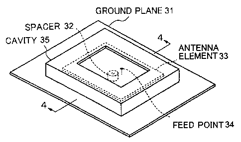
FIG. 3 is a perspective view illustrating a
structure of a planar antenna device according to the
present invention. FIG. 4 is a sectional view taken
along the line 4-4 of FIG. 3.
In FIG. 3, an antenna element 33 is mounted above
a ground plane 31 via a spacer 32 so that the antenna
element 33 is separated from the ground plane 31. This
antenna element 33 is excited by power from the feed
point 34. The ground plane 31 is made of a metal plate
such as brass, aluminum, stainless steel, and the like.
The spacer 32 is made of synthetic resin such as
polyacetal, polycarbonate, ABS, and the like. The
antenna element 33 is made of a metal plate such as
brass, aluminum, and the like.
A box-like cavity 35 is placed on the ground plane
31 so as to cover the entire antenna element 33. The
cavity 35 is made of a metal plate such as brass,
aluminum, and the like.
The cavity 35 is provided so that it does not
touch the antenna element 33 with a predetermined
distance. A square opening 35a, which is smaller than
a size of the antenna element 33, is formed at a
surface a cavity 35 which is opposite to the antenna
element 33.
The opening 35a of this cavity 35 is formed in
order to provide high electromagnetic field radiation
CA 02329458 2000-12-21
_ 7 _
characteristics in a wide range of elevation angles,
especially toward a low elevation angle without
reducing the size of the antenna element 33. It is
possible to change electromagnetic field radiation
characteristics especially toward a low elevation angle
by adjusting the size of the opening 35a with reference
to the antenna element 33 and a distance between the
opening 35a and the antenna element 33.
In the above-mentioned antenna device structure,
various characteristics observed from experiments will
be described as follows.
First, characteristics of the antenna device
itself will be described with reference to FIGS. 6
through 7.
FIGS. 5 through 7 show an experimental voltage
standing-wave ratio (VSWR), a return loss corresponding
to the VSwR, and a Smith chart, respectively. Any of
the characteristics FIGS. 5 through 7 indicates that an
excellent performance is available at approximately
2.34 GHz with an input impedance of 50~.
FIGS. 8 through 9C exemplify characteristics of
the antenna device according to the embodiment of the
present invention in comparison with the air patch
antenna device in FIG. 1 and the dielectric patch
antenna device in FIG. 2.
FIG. 8 shows gain characteristics corresponding to
azimuth angles at a horizontal plane. A characteristic
CA 02329458 2000-12-21
a indicated by a thin line corresponds to the air
patch antenna device in FIG. 1. A characteristic
indicated by a broken line corresponds to the
dielectric patch antenna device in FIG. 2. A
characteristic y indicated by thick lines corresponds
to the antenna device with the cavity 35 in FIGS. 3 and
4 according to this embodiment.
As shown in FIG. 8, the air patch antenna device
showing the characteristic a provides a high gain at
around azimuth angle 0°, but causes large gain changes
corresponding to azimuth angles. The air patch antenna
device in FIG. 8 is found to be inappropriate for,
especially, an on-vehicle antenna device which always
changes antenna device angles according to directions
of radio waves received.
The dielectric patch antenna device showing the
characteristic a decreases the antenna element size
and causes a dielectric loss, decreasing the total gain
for the entire antenna device.
By contrast, the antenna device according to this
embodiment showing the characteristic y causes a
little change in gains according to azimuth angles and
is found to be suited for an antenna device which
always changes antenna device angles in accordance with
directions of radio waves received.
FIGS. 9A through 9C show directivities of the
antenna devices explained in FIG. 8.
CA 02329458 2000-12-21
- 9 -
FIG. 9A exemplifies a directivity of the air patch
antenna device. The directivity is valid only in a
front direction and within a high elevation angle range.
It is understood that the directive range is very
narrow.
FIG. 9B exemplifies a directivity of the
dielectric patch antenna device. Compared to the air
patch antenna device in FIG. 9A, the dielectric patch
antenna device in FIG. 9B increases a characteristic at
the azimuth angle and toward a low elevation angle.
However, it is understood that the directivity is
unsatisfactory.
FIG. 9C exemplifies a directivity of the antenna
device with the cavity 35 according to this embodiment.
The antenna device in FIG. 9C provides the directivity
in a very wide range not only at the azimuth angle on
the horizontal plane, but also at elevation angles
especially ranging from low to high elevation-angle
directions.
As mentioned above, the antenna device structure
with the cavity 35 according to this embodiment of the
present invention can maintain high electromagnetic
field radiation characteristics over a wide elevation
angle range from a low elevation-angle direction. It
is also possible to provide a sufficiently high total
gain for the entire antenna device.
Compared to a quadrifilar helical antenna device,
CA 02329458 2000-12-21
- 10 -
a cross di-pole antenna device, and the like having
high efficiency and low elevation-angle radiation
characteristics, the antenna device according to this
embodiment of the present invention provides the
following advantages.
(1) Simplifying a structure of the entire antenna
device including a feed structure.
(2) Providing a mechanically solid structure
having the rigid cavity for guarding the antenna
element with no sharp projections.
(3) Easily manufacturing the antenna device.
(4) Easily thinning the entire antenna device
structure.
The antenna device according to the present
invention can be easily mass-produced and be suitably
mounted on vehicles such as cars.
The above-mentioned embodiment provides an air
patch antenna device with the cavity 35. The present
invention is not limited thereto.
For example, in the embodiment, an elevation
radiation characteristic is improved by providing the
cavity, but a rectangular conductor 36 having an
opening (or may be a circular conductor, or a linear
conductor like a wire etc.) as shown in FIG. 10 may be
provided like the cavity 35. That is, any conductor
may be used to define an aperture of the antenna. With
this configuration, the same advantage can be obtained
CA 02329458 2000-12-21
- 11 -
as the above-mentioned embodiment.
The present invention is not limited to above-
mentioned embodiment, and can be achieved in a scope of
the invention.
Additional advantages and modifications will
readily occur to those skilled in the art. Therefore,
the invention in its broader aspects is not limited to
the specific details and representative embodiments
shown and described herein. Accordingly, various
modifications may be made without departing from the
spirit or scope of the general inventive concept as
defined by the appended claims and their equivalents.