Note: Descriptions are shown in the official language in which they were submitted.
CA 02329542 2000-10-20
-1-
SYSTEM AND METHOD FOR SCHEDULING MESSAGE TRANSMISSION AND PROCESSING IN A
DIGITAL DATA NETWORK
FIELD OF THE INVENTION
The invention relates generally to the field of digital communications systems
and more particularly
to digital networks for facilitating communication of digital data in, for
example, digital image, audio
and video distribution systems and among digital computer systems. The
invention is more
particularly directed to flow control and scheduling arrangements for
regulating the flow of
information through the network to avoid congestion, prevent loss of data and
preserve fairness
among a plurality of devices that are transferring information over the
network.
BACKGROUND OF THE INVENTION
Digital networks have been developed to facilitate the transfer of
information, including data
and programs, among digital computer systems and other digital devices. A
variety of types of
networks have been developed and implemented using diverse information
transfer methodologies.
In some networks, such as the well-known Ethernet, a single wire is used to
interconnect all of the
devices connected to the network. While this simplifies wiring of the network
in-a facility and
connection of the devices to the network, it results in generally slow
information transfer, since the
wire can only carry information, in the form of messages, from a single device
at a time. To alleviate
this to some extent, in some Ethernet installations, the network is divided
into a number of sub-
networks, each having a separate wire, with interfaces interconnecting the
wires. In such
installations, wires can carry messages for devices connected thereto
simultaneously, which increases
the number of messages that can be transferred simultaneously. It is only when
a device connected
to one wire needs to send a message to a device connected to another wire that
wires in two or more
sub-networks will be used, making them unavailable for use by other devices
connected thereto.
To further alleviate this, networks have been developed in which
communications are
handled through a mesh of switching nodes. The computer systems and other
devices are connected
to various switching nodes. Since the switching nodes themselves are
interconnected in a variety
of patterns, a number of paths may be available between pairs of the devices,
so that if one path is
congested, another may be used. Such an arrangement may result in a network
which is more
complicated than an Ethernet network, but it can provide substantially higher
information transfer
CA 02329542 2000-10-20
-2-
rates, particularly if optical fiber is used as the media interconnecting the
switching nodes and
devices. A problem which may arise with such networks is that, in such
networks, a switching node
or a device, when it is receiving information from another switching node or
device in the network,
does not have a mechanism to provide "flow-control" information to the
transmitting switching node
or device. While this does reduce the cost of a network, it may result in
congestion, in which either
a switching node may receive information at a rate faster than it can transmit
it, or a destination
device may receive information at a rate faster than it can buffer and process
it.
SUMMARY OF THE INVENTION
The invention provides a new and improved system and method for scheduling the
transfer
of messages in a communications network.
In brief summary, the invention in one embodiment provides a system comprising
at least
two devices interconnected by a network including at least one communication
link. Each device
includes a network interface for transferring messages over the network. At
least one of the devices
as a source device, transmits messages over one or more virtual circuits
established over the network,
and at least one other of said devices, as a destination device for the
respective virtual circuits,
receives the messages thereover. The network interface of the source device
includes a transmit
section that includes a transmitter and a transmit scheduler. The transmitter
generally transmits
messages for the respective virtual circuits for which the device is the
source device. The transmit
scheduler schedules transmission of messages by the transmitter so that
messages are transmitted in
a round-robin manner as among the virtual circuits for which the device is the
source device, thereby
providing fairness in message transmission as among the virtual circuits. In
one embodiment, the
transmitter transmits messages in a series of fixed-length cells, each of
which can contain a portion
of a message, and the transmit scheduler schedules transmission of messages by
the transmitter so
that messages are transmitted in a round-robin manner as among the virtual
circuits for which the
device is the source device, so that short messages for ones of the virtual
circuits are not unduly
delayed by relatively long messages for others of the virtual circuits. The
network interface of the
destination device includes a receive host for performing predetermined
operations in connection
with receive messages, and a receive scheduler. The receive scheduler
schedules the virtual circuits
for which the device is the destination device and enables the receive host to
perform the
predetermined operations in connection with the virtual circuits for which the
device is the
CA 02329542 2007-07-30
-3-
destination device in a round-robin manner, thereby providing fairness in
message processing as
among the virtual circuits.
In another embodiment, the network includes a switching node which forms part
of the path
for one or more virtual circuits between the source device and the destination
device. The switching
node is connected to receive messages transmitted by the source device over
the virtual circuit(s) for
which it forms part of the path over one communication link connected thereto,
buffer the received
messages in an internal buffer, and transmit the buffered messages over the
virtual circuit(s) over
another communication link connected thereto, thereby to forward messages for
the virtual circuit(s)
downstream over the respective virtual circuit(s). The switching node
transmits the buffered
messages over the virtual circuits generally in a round-robin manner for
virtual circuits for which the
respective communication link forms part of the path, thereby providing
fairness in message
transmission as among the virtual circuits.
In accordance with another aspect of the present invention, there is provided
a system
comprising: source and destination devices interconnected by a network
including at least one
communication link, the source device being operable to transmit message
packets over one or
more virtual circuits established over the network to the destination device,
the destination device
being operable to receive the message packets thereover,
A. the source device comprising a transmit section that comprises a
transmitter and a
transmit scheduler, the transmitter being configured to transmit message
packets for the respective
virtual circuits for the source device, and the transmit scheduler being
configured to schedule
transmission of inessage packets by the transmitter so that messages are
transmitted in a round-
robin manner as among ones of the virtual circuits; and
B. a destination device comprising:
(a) a receive buffer operable to store linked lists of data from received
message
packets, each linked list corresponding to a specific virtual circuit,
(b) a memory,
(c) a receive host operable to transfer data from the receive buffer to the
memory of
the destination device and
(d) a receive scheduler, configured to schedule high priority virtual circuits
in a
round-robin manner and low priority virtual circuits in a round-robin manner
for the receive host to
transfer data from the receive buffer to the memory.
CA 02329542 2007-07-30
-3a-
In accordance with yet another aspect of the present invention, there is
provided a system
comprising at least two devices interconnected by a network including at least
one communication
link, each device including a network interface for transferring message
packets over the network,
at least one of the devices as a source device, transmitting message packets
over one or more virtual
circuits established over the network, and at least one other of said devices,
as a destination device
for the respective virtual circuits, receiving the message packets thereover,
A. the network interface of the source device including a transmit section
that includes
a transmitter and a transmit scheduler, the transmitter being configured to
transmit message packets
for the respective virtual circuits for which the device is the source device,
and the transmit
scheduler being configured to schedule transmission of message packets by the
transmitter so that
messages are transmitted in a round-robin manner as among ones of the virtual
circuits for which
the device is the source device; and
B. the network interface of the destination device including a receive host
for
performing predetermined operations in connection with received message
packets, and a receive
scheduler, the receive scheduler being configured to schedule the virtual
circuits for which the
device is the destination device to enable the receive host to perform the
predetermined operations
in connection with the virtual circuits for which the device is the
destination device in a round-
robin manner; the transmit scheduler includes:
A. a virtual circuit task list configured to identify virtual circuits for
which message
packets are to be transmitted; and
B. a transmit task control configured to sequence through the virtual circuit
task list
to identify successive virtual circuits for which message packets are to be
transmitted and, for each
identified virtual circuit, to enable data to be obtained for transmission by
said transmitter in a
respective message packet;
wherein said virtual circuit task list is configured to include a plurality of
prioritized
task lists, the transmit task control being configured to select among said
prioritized task lists and,
for each prioritized task list so selected, identify a virtual circuit for
which message packets are to
be transmitted; in which each virtual circuit is identified by a virtual
circuit identifier, the virtual
circuit identifiers each having a value within a range of virtual circuit
identifier values, each of said
prioritized task lists comprising a bit map including a bit associated with
each virtual circuit
identifier value in said range, the transmit task control being configured to,
for each virtual circuit
CA 02329542 2007-07-30
-3b-
for which a message packet is to be transmitted at the respective priority
level, set the bit in the bit
map of the respective prioritized task list associated with the virtual
circuit's virtual circuit identifier
value, the transmit task control using the set bits to identify virtual
circuits for which message
packets are to be transmitted.
In accordance with still another aspect of the present invention, there is
provided a system
comprising at least two devices interconnected by a network including at least
one communication
link, each device including a network interface for transferring message
packets over the network,
at least one of the devices as a source device, transmitting message packets
over one or more virtual
circuits established over the network, and at least one other of said devices,
as a destination device
for the respective virtual circuits, receiving the message packets thereover,
A. the network interface of the source device including a transmit section
that includes
a transmitter and a transmit scheduler, the transmitter being configured to
transmit message packets
for the respective virtual circuits for which the device is the source device,
and the transmit
scheduler being configured to schedule transmission of message packets by the
transmitter so that
messages are transmitted in a round-robin manner as among ones of the virtual
circuits for which
the device is the source device; and
B. the network interface of the destination device including a receive host
for
performing predetermined operations in connection with received message
packets, and a receive
scheduler, the receive scheduler being configured to schedule the virtual
circuits for which the
device is the destination device to enable the receive host to perform the
predetermined operations
in connection with the virtual circuits for which the device is the
destination device in a round-
robin manner;
wherein the transmit scheduler includes:
A. a virtual circuit task list configured to identify virtual circuits for
which
message packets are to be transmitted; and
B. a transmit task control configured to sequence through the virtual circuit
task
list to identify successive virtual circuits for which message packets are to
be transmitted and, for
each identified virtual circuit, to enable data to be obtained for
transmission by said transmitter in a
respective message packet;
wherein said virtual circuit task list is configured to include a plurality of
prioritized
CA 02329542 2007-07-30
- 3c-
task lists, the transmit task control being configured to select among said
prioritized task lists and,
for each prioritized task list so selected, identify a virtual circuit for
which message packets are to
be transmitted; in which one or more message packets are associated with a
message, each message
having a beginning, one of said prioritized task lists being associated with
virtual circuits for which
data for message packets associated with the beginning of a message is to be
obtained and another
of said prioritized task lists being associated with virtual circuits for
which data for message
packets associated with the beginning of a message have been obtained, the
transmit task control
being configured to select from each of said prioritized task lists at a
selected rate.
In accordance with still yet another aspect of the present invention, there is
provided a
system comprising at least two devices interconnected by a network including
at least one
communication link, each device including a network interface for transferring
message packets
over the network, at least one of the devices as a source device, transmitting
message packets over
one or more virtual circuits established over the network, and at least one
other of said devices, as a
destination device for the respective virtual circuits, receiving the message
packets thereover,
A. the network interface of the source device including a transmit section
that includes
a transmitter and a transmit scheduler, the transmitter being configured to
transmit message packets
for the respective virtual circuits for which the device is the source device,
and the transmit
scheduler being configured to schedule transmission of message packets by the
transmitter so that
messages are transmitted in a round-robin manner as among ones of the virtual
circuits for which
the device is the source device; and
B. the network interface of the destination device including a receive host
for
performing predetermined operations in connection with received message
packets, and a receive
scheduler, the receive scheduler being configured to schedule the virtual
circuits for which the
device is the destination device to enable the receive host to perform the
predetermined operations
in connection with the virtual circuits for which the device is the
destination device in a round-
robin manner; in which the receive scheduler includes:
A. a virtual circuit task list configured to identify virtual circuits for
which
message packets have been received; and
B. a receive task control configured to sequence through the virtual circuit
task
list to identify successive virtual circuits for which message packets have
been received, and, for
each identified virtual circuit, to enable data to be transferred to a data
store; in which said virtual
CA 02329542 2007-07-30
-3d-
circuit task list is configured to include a plurality of prioritized task
lists, the receive task control
being configured to select among said prioritized task lists and, for each
prioritized task list so
selected, identify a virtual circuit for which data will be transferred to a
data source; in which each
virtual circuit is identified by a virtual circuit identifier, the virtual
circuit identifiers each having a
value within a range of virtual circuit identifier values, each of said
prioritized task lists comprising
a bit map including a bit associated with each virtual circuit identifier
value in said range, the
receive task control being configured to, for each virtual circuit for which a
message packet has
been received, set the bit in the bit map of an appropriate one of the
respective prioritized task lists
associated with the virtual circuit's virtual circuit identifier value, the
receive task control using a
set bit to identify a virtual circuit for which data will be transferred to a
data store.
In accordance with still a further aspect of the present invention, there is
provided a system
comprising at least two devices interconnected by a network including at least
one communication
link, each device including a network interface for transferring message
packets over the network,
at least one of the devices as a source device, transmitting message packets
over one or more virtual
circuits established over the network, and at least one other of said devices,
as a destination device
for the respective virtual circuits, receiving the message packets thereover,
A. the network interface of the source device including a transmit section
that includes
a transmitter and a transmit scheduler, the transmitter being configured to
transmit message packets
for the respective virtual circuits for which the device is the source device,
and the transmit
scheduler being configured to schedule transmission of message packets by the
transmitter so that
messages are transmitted in a round-robin manner as among ones of the virtual
circuits for which
the device is the source device; and
B. the network interface of the destination device including a receive host
for
performing predetermined operations in connection with received message
packets, and a receive
scheduler, the receive scheduler being configured to schedule the virtual
circuits for which the
device is the destination device to enable the receive host to perform the
predetermined operations
in connection with the virtual circuits for which the device is the
destination device in a round-
robin manner; in which the receive scheduler includes:
A. a virtual circuit task list configured to identify virtual circuits for
which
message packets have been received; and
B. a receive task control configured to sequence through the virtual circuit
task
CA 02329542 2007-07-30
-3e-
list to identify successive virtual circuits for which message packets have
been received, and, for
each identified virtual circuit, to enable data to be transferred to a data
store; in which said virtual
circuit task list is configured to include a plurality of prioritized task
lists, the receive task control
being configured to select among said prioritized task lists and, for each
prioritized task list so
selected, identify a virtual circuit for which data will be transferred to a
data source; in which said
network interface of said destination device further includes a buffer for
buffering received
message packets, one of said prioritized task lists being associated with
virtual circuits for which
the buffer contains at least one message packet associated with a virtual
circuit and another of said
prioritized task lists being associated with virtual circuits for which the
buffer contains message
packets associated with a virtual circuit at a selected buffer congestion
level, the receive task
control being configured to select from each of said prioritized task lists at
a selected rate.
In accordance with an even further aspect of the present invention, there is
provided a
system comprising: source and destination devices interconnected by a network
including at least
one communication link, the source device being operable to transmit message
packets over one or
more virtual circuits established over the network to the destination device,
the destination device
being operable to receive the message packets thereover,
A. the source device comprising a transmit section that comprises a
transmitter and a
transmit scheduler, the transmitter being configured to transmit message
packets for the respective
virtual circuits for the source device, and the transmit scheduler being
configured to schedule
transmission of message packets by the transmitter so that messages are
transmitted in a round-
robin manner as among ones of the virtual circuits; and
B. the destination device comprising
(a) a receive buffer operable to store data from received message packets,
(b) a memory,
(c) a receive host operable to transfer data from the receive buffer to the
memory of
th-, destination device, and
(d) a receive scheduler configured to schedule virtual circuits in a round-
robin
manner for the receive host to transfer data from the receive buffer to the
memory;
the transmit scheduler comprising:
CA 02329542 2007-07-30
-3f-
A. a virtual circuit task list configured to identify virtual circuits for
which
message packets are to be transmitted; and
B. a transmit task control configured to sequence through the virtual circuit
task
list to identify successive virtual circuits for which message packets are to
be transmitted and, for
each identified virtual circuit, to enable data to be obtained for
transmission by said transmitter in a
respective message packet; said virtual circuit task list being configured to
include a plurality of
prioritized task lists, the transmit task control being configured to select
among said prioritized task
lists and, for each prioritized task list so selected, identify a virtual
circuit for which message
packets are to be transmitted; wherein the prioritized task lists comprise a
memory configured to
store identifications of virtual circuits with pending doorbell tasks.
In accordance with still a further aspect of the present invention, there is
provided a system
comprising: source and destination devices interconnected by a network
including at least one
communication link, the source device being operable to transmit message
packets over one or
more virtual circuits established over the network to the destination device,
the destination device
being operable to receive the message packets thereover,
A. the source device comprising a transmit section that comprises a
transmitter and a
transmit scheduler, the transmitter being configured to transmit message
packets for the respective
virtual circuits for the source device, and the transmit scheduler being
configured to schedule
transmission of message packets by the transmitter so that messages are
transmitted in a round-
robin manner as among ones of the virtual circuits; and
B. the destination device comprising
(a) a receive buffer operable to store data from received message packets,
(b) a memory,
(c) a receive host operable to transfer data from the receive buffer to the
memory of
the destination device, and
(d) a receive scheduler configured to schedule virtual circuits in a round-
robin
manner for the receive host to transfer data from the receive buffer to the
memory;
the transmit scheduler comprising:
A. a virtual circuit task list configured to identify virtual circuits for
which
CA 02329542 2007-07-30
-3g-
message packets are to be transmitted; and
B. a transmit task control configured to sequence through the virtual circuit
task
list to identify successive virtual circuits for which message packets are to
be transmitted and, for
each identified virtual circuit, to enable data to be obtained for
transmission by said transmitter in a
respective message packet; said virtual circuit task list being configured to
include a plurality of
prioritized task lists, the transmit task control being configured to select
among said prioritized task
lists and, for each prioritized task list so selected, identify a virtual
circuit for which message
packets are to be transmitted; wherein the prioritized task lists comprise a
first memory configured
to store identifications of virtual circuits with pending high priority data
retrievals, and a second
memory configured to store identifications of virtual circuits with pending
low priority data
retrievals.
BRIEF DESCRIPTION OF THE DRAWINGS
This invention is pointed out with particularity in the appended claims. The
above and
further advantages of this invention may be better understood by referring to
the following
description taken in conjunction with the accompanying drawings, in which:
FIG. 1 schematically depicts a computer network in which a flow control
arrangement in
accordance with the invention is implemented;
FIG. 2 is a functional block diagram of a computer system for use in the
computer network
depicted in FIG. 1;
FIG. 3 is a functional block diagram of a switching node for use in the
computer network
depicted in FIG. 1;
FIG. 4 is a flowchart detailing operations of a computer system in connection
with the
invention; and
FIGS. 5 and 6 are functional block diagrams of receive and transmit schedulers
for use in
connection with the computer system depicted in FIG. 2.
DETAILED DESCRIPTION OF AN ILLUSTRATIVE EMBODIMENT
FIG. 1 schematically depicts a computer network 10 including a plurality of
switching nodes
11(1) through I 1(N) (generally identified by reference numeral 11(n)) for
transferring signals
representing data among a number of devices, which in FIG. 1 are represented
by computers 12(1)
through 12(M) (generally identified by reference numeral 12(m)). The computers
12(m), as is
CA 02329542 2000-10-20
-4-
conventional, process data, in accordance with theirprogram instructions to
generate processed data.
In their processing, a computer 12(ms ) (subscript "S" referencing "source")
may, as a source
computer, need to transfer data, processed data and/or program instructions
(all of which will be
referred to herein generally as "information") to another, destination,
computer 12(mD) (subscript "D"
referencing "destination"), which may need to use the transferred information
in its operations. Each
computer 12(m) is connected over a communication link, generally identified by
reference numeral
13(p), to a switching node 11(n) to facilitate transmission of data thereto or
the reception of data
therefrom. The switching nodes 11(n) receive, buffer and forward data received
from the computers
11(n) and from other switching nodes 11(n) to facilitate the transfer of data
among the computers
12(m). The switching nodes 11(n) are interconnected by communication links,
also generally
identified by reference numeral 13(p) to facilitate the transfer of data
thereamong. The
communication links 13(p) may utilize any convenient data transmission medium.
Each
communication link 13(p) depicted in FIG. 1 is preferably bi-directional,
allowing the switching
nodes 11(n) to transmit and receive signals among each other and with
computers 12(m) connected
thereto over the same link; to accommodate bi-directional communication links,
separate media may
be provided for each communication link 13(p), each of which facilitates
unidirectional transfer of
signals thereover.
In one embodiment, the data is transferred using the well-known "ATM"
("Asynchronous
Transfer Mode") transfer methodology. That methodology is described in detail
in C. Partridge,
Gigabit Networking, (Reading MA: Addison Wesley Publishing Company, 1994),
primarily in
chapters 3 and 4, and D. McDysan, et al., ATM Theorv And Application (McGraw
Hill, 1995) and
will not be described in detail. Generally, in the ATM methodology, the
computers 12(m) and the
switching nodes 11(n) transmit data in the form of fixed-length "cells" over
"virtual circuits"
established between computers 12(m) through the network. Each virtual circuit
essentially defines
a path from a source computer 12(ms) to a destination computer 12(mD) through
one or more
switching nodes 11(n) and over respective communication links 13(p). In the
ATM data transfer
methodology, for a block of inforrnation to be transferred from a source
computer 12(mS) to a
destination computer 12(mD) over a virtual circuit established therebetween,
the source computer
12(ms) allocates the data block to one or a series of "cells" for transmission
serially over the
communication link 13(p). Each cell transferred through the network 10
includes a header portion
and a data portion, with the header portion including virtual circuit
identifier information for
CA 02329542 2000-10-20
-5-
controlling the transfer of the cell through the network 10, along with
protocol and other control
information, including an "end of message" ("EOM") flag. The data portion
contains data from the
data block that is to be transferred in the cell. The data portion of each
cell is of fixed, predetermined
length, which, in one embodiment, is forty-eight bytes. The source computer
12(ms) will pad the
data in the data portion of the cell (if one cell will accommodate the data
block to be transferred) or
the last cell in the series (if multiple cells are required to accommodate the
data block to be
transferred) if the amount of data in the block is not an integral multiple of
the size of the data
portion of each cell to ensure that the data portion of the last cell has the
required length. If a series
of cells are required to transfer a data block, the source computer 12(ms)
will transmit the cells so
that the data in the data portions of the series of cells to conform. to the
order of data in the data block
that is being transferred. In addition, if that cells are properly transferred
to the destination computer
12(mD), the destination computer will receive the cells in the same order. In
the last cell in a series
which contains information from a data block, the end of message flag in the
header portion is set,
thereby to notify the destination computer 12(mD) that it has received all of
the cells containing data
for the data block.
The invention provides an arrangement for enabling the computers 12(m) and
switching
nodes 11(n) to control the flow of cells over the network to avoid or reduce
the likelihood that
congestion will develop both at the switching nodes 11(n) and at the
destination computer, which
may otherwise lead to degradation in the cell transfer throughput or loss of
cells in the network. The
invention further provides an arrangement for scheduling operations by the
computers 12(m) and
switching nodes 11(n) to generally facilitate fairness in the transfer of
information and reasonable
latency in the transfer of small messages over the various virtual circuits
established through the
network 10. Generally, in connection with flow control, the computers 12(m)
and switching nodes
11(n) implement flow control in two modes, identified herein as a virtual
circuit flow control mode
and a link flow control mode. In the virtual circuit flow control mode, if a
computer 12(m),
operating as destination computer 12(mD) for a virtual circuit, is receiving
cells associated with the
virtual circuit at rate that is too fast for it to process (as will be
described below), the destination
computer 12(mD), operating in the virtual circuit flow control mode, will
enter a set virtual circuit
flow control state in which it enables flow control for the virtual circuit.
In that operation, the
destination computer 12(mD) will generate a set virtual circuit flow control
message and transmit it
upstream along the path for the virtual circuit, that is towards the source
computer 12(ms) for the
CA 02329542 2000-10-20
-6-
virtual circuit. Each switching node 11(n) along the path for the virtual
circuit from the destination
computer 12(mD) to the source computer 12(ms) will also enter a set virtual
circuit flow control state
for the virtual circuit. When the source computer 12(mS) for the virtual
circuit receives the set virtual
circuit flow control message, it will effectively stop transmitting cells
associated with that virtual
circuit.
Each switching node 11(n) along the path for the virtual circuit, if it is
receiving cells
associated with the virtual circuit at a rate that is, for example, too fast
for it to forward downstream
along the path for the virtual circuit (as also described below), can also,
operating in the virtual
circuit flow control mode, enter a set virtual circuit flow control state and
generate a set virtual
circuit flow control message and transmit it upstream along the path for the
virtual circuit. The
upstream switching nodes 11(n), if any, along the path for the virtual circuit
to the source computer
12(mS), and source computer 11(mS), will operate in the same manner as
described above.
When the destination computer 12(mD) can resume receiving cells for that
virtual circuit, it
will enter a clear virtual circuit flow control state, in which it will
generate a clear virtual circuit flow
control message and transmit it upstream along the path for the virtual
circuit. If a switching node
11(n) receives the clear virtual circuit flow control message and it is not
itself in the set virtual circuit
flow control state, it will forward the set virtual circuit flow control
message upstream-along the path
for the virtual circuit to the upstream switching node 11(n), if any, along
the path to the source
computer 12(mS), or to the source computer 12(mS) for the virtual circuit. On
the other hand, if a
switching node 11(n) receives the clear virtual circuit flow control message
and it is itself in the set
virtual circuit flow control state, it will delay forwarding the clear virtual
circuit flow control
message until it leaves the set virtual circuit flow control state, at which
point it will forward the
clear virtual circuit flow control message upstream along the path for the
virtual circuit. When the
source computer 12(ms) receives a clear virtual circuit flow control message,
it can resume
transmitting cells associated with the virtual circuit downstream over the
virtual circuit. It will be
appreciated that, by allowing a switching node 11(n) to delay forwarding of
the clear virtual circuit
flow control message upstream along the path for the virtual circuit while it
is in the set virtual
circuit flow control state, that will allow the switching node 11(n) to
forward cells for the virtual
circuit and thereby reduce the number of cells that it may have been buffering
for the virtual circuit,
before enabling an upstream switching node 11(n) or the source computer 12(ms)
to resume
transmitting cells thereto.
CA 02329542 2000-10-20
-7-
The link flow control mode is implemented on a communication link-basis,
instead of on a
per-virtual circuit basis. Thus, in the link flow control mode, if a computer
12(m) is receiving cells
from the switching node 11(n) connected thereto at rate that is too fast for
it to process (as will also
be described below), the computer 12(m), operating in the link flow control
mode, will enter a set
link flow control state in which it enables flow control for the communication
link. In that operation,
the computer 12(m) will generate a set link flow control message and transmit
it to the switching
node 11(n) connected thereto over that link. When the switching node 11(n)
receives the set link
flow control message, it will stop transmitting cells thereto overthat link.
Similarly, each switching
node 11(n), if it is receiving cells at a rate that is, for example, too fast
for it to forward (as also
described below), it can also, operating in the link flow control mode, enter
a set link flow control
state and generate respective set link flow control messages and transmit them
other switching nodes
11(n) or computers 12(m) connected thereto which are transmitting cells
thereto; when those
switching nodes 11(n) or computers 12(m) receive the set link flow control
messages, they will also
stop transmitting cells to the switching node 11(n) from which the respective
set link flow control
message was received.
When the computer 12(m) can resume receiving cells from the switching node
11(n) over the
communication link 13(p), it will enter a clear link flow control state and
generate a clear link flow
control message and transmit it to the switching node 11(n). When the
switching node 11(n) receives
the clear link flow control message, it can resume transmitting cells to the
computer 12(m).
Similarly, when a switching node 11(n) operating in the set link flow control
state can resume
receiving cells, it can enter a clear link flow control state, generate
respective clear link flow control
message and transmit them to switching nodes 11(n) and/or computers 12(m)
connected thereto. In
either case, the switching nodes 11(n) and computers 12(m), after receiving
respective clear link flow
control messages, can resume transmitting cells to the switching node 11(n) or
computer 12(m) from
which they received the clear link flow control messages.
Providing separate virtual circuit flow control and link flow control modes
provides several
benefits. For example, the virtual circuit flow control mode can be used to
provide general fairness
for cell transmission bandwidth through the network as among virtual circuits
which terminate at
each destination computer 12(mD) or for which each switching node 11(n) forms
part of the path.
The virtual circuit flow control mode can also be used to reduce the
likelihood that excessive
congestion will develop. On the other hand, the link flow control mode can be
used if excessive
CA 02329542 2000-10-20
-8-
congestion does develop, to prevent, or at least reduce the likelihood that,
cells will be received by
a computer 12(m) or switching node 11(n) at a rate which will overflow buffers
provided thereby,
which, in turn, can lead to cell loss. In one embodiment, the various flow
control messages, that is,
set and clear virtual circuit flow control messages and set and clear link
flow control messages are
relatively short, including a message type flag that identifies the type of
message, that is, a set virtual
circuit flow control message, a clear virtual circuit flow control message, a
set link flow control
message and a clear virtual circuit message, and an identifier portion. If the
identifier portion
contains a predetermined value, which in one embodiment is "zero," the message
is a set or clear link
flow control message, depending on the value of the message type flag. On the
other hand, if the
identifier portion contains a value other than the predetermined value, the
message is a set or clear
virtual circuit flow control message, also depending'on the value of the
message type flag, with the
value in the identifier portion identifying the virtual circuit with which it
is associated. Since the set
and clear virtual circuit and link flow control messages are relatively short,
only a small amount of
bandwidth through the network is required to transfer them.
Before proceeding to a detailed description of the flow control arrangement
used in system
10, it would be helpful to describe the structure and operation of computer
12(m) and switching node
11(n) used in one embodiment of system 10. FIG. 2 depicts a functional
block.diagram of a
computer 12(m) for use in connection with the network 10, and FIG. 3 depicts a
functional block
diagram of a switching node 11(n) for use in connection with network 10.
Generally, a computer
12(m) may comprise any type ofconventional computer, including a conventional
personal computer
or computer workstation, server computer, mini- or mainframe computer, or the
like. With reference
to FIG. 2, computer 12(m) includes a processor 20, system memory 21, mass
storage subsystem 22,
input/output subsystem 23 and a network interface 24 all interconnected by an
interconnection
arrangement 25. In one embodiment, the interconnection arrangement 25 includes
a conventional
PCI bus. The processor 20 processes one or more application programs under
control of an operating
system. In specific connection with transfers of data over the network 10,
(i) for transfers in which the computer 12(m) operates as a source computer
12(ms), the
processor can establish buffers (not separately shown) in the system memory 21
in which it loads
blocks of data to be transferred to other computers as destination computers
12(mD), and
CA 02329542 2000-10-20
-9-
(ii) for transfers in which the computer 12(m) operates as a destination
computer 12(mD) the
processor can establish buffers (also not separately shown) in the system
memory in which blocks
of data received from other computer as source computers 12(ms),
as described, for one embodiment, in the Virtual Interface Architecture
("VIA") specification,
Version 1(December 16, 1997), published by Compaq Computer Corp., Intel Corp.
and Microsoft
Corp.
The mass storage subsystem generally provides long-term storage for
information which may
be processed by the processor 20. The mass storage subsystem 22 may include
such devices as disk
or tape subsystems, optical disk storage devices and CD-ROM devices in which
information may
be stored and/or from which information may be retrieved. The mass storage
subsystem 22 may
utilize removable storage media which may be rerrioved and installed by an
operator, which may
allow the operator to load programs and data into the computer 12(m) and
obtain processed data
therefrom.
The input/output subsystem 23 includes operator input and output subsystems
that generally
provide an operator interface to the digital computer 10. In particular,
operator input subsystems
may include, for example, keyboard and mouse devices, which an operator may
use to interactively
input information to the digital computer 10 for processing. In addition, the
operator input
subsystems may provide mechanisms whereby the operator may control the digital
computer 10.
The operator output subsystems may include devices such as video display
devices, through which
the digital computer 10, under control of the microprocessor 11, displays
results of processing to the
operator. In addition, a printer may be provided to provide a hardcopy output
for the operator.
The network interface 24 retrieves data from the system memory 21 that is to
be transferred
to other computers operating as destination computers 12(mD), generates cells
therefrom and transfers
the generated cells over the communication link 13 (p). In addition, the
network interface 24 receives
cells from the communication link 13(p), extracts the data therefrom and
transfers the data to
appropriate buffers in the system memory 21 for storage. The network interface
24 includes a
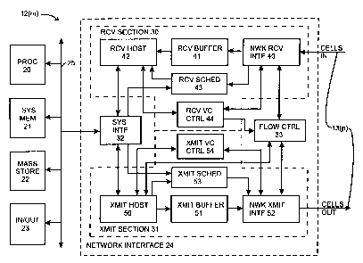
number of components, including a receive section 30, a transmit section3 1, a
system interface
circuit 32 and a flow control circuit 33. The receive section 30 connects to
the communication link
13(p) and receives cells received thereover, buffers the data from the
received cells, and cooperates
with the system interface circuit 32 to transfer the buffered data over
interconnection arrangement
25 to the system memory 21 for storage for use by applications being processed
by the computer
CA 02329542 2000-10-20
-10-
12(m). The transmit section 31 cooperates with the system interface circuit 32
to retrieve data to be
transmitted from the system memory 21 over interconnection arrangement 25,
generates cells and
transmits them over the communication link 13(p). In one embodiment, the
system interface circuit
32 operates in a DMA (direct memory access) manner to retrieve data from the
system memory 21
for transmission by the transmit section 31, and to transfer data received by
the receive section 30
to the system memory 21 for storage. The system interface circuit 32 also
operates to receive control
information from the processor 20 for storage in various control registers
(not shown) which control
operations ofthe receive section 30, transmit section 31, flow control circuit
33 as well as the system
interface circuit 32 itself.
As noted above, the receive section 30 operates to receive cells from the
communication link
13(p) that is connected to the computer 12(m), buffer the data from the
received cells and, in
cooperation with the system interface circuit 32, transfer the buffered data
to the system memory 21
for storage. The receive section includes a number of components, including a.
network receive
interface circuit 40, a receive buffer 41, a receive host circuit 42, a
receive scheduler 43 and a receive
virtual circuit control circuit 44. The network receive interface circuit 40
receives cells, identified
as "CELLS IN" from the communication link 13(p) connected to the computer
12(m) and buffers
the data in the data portion of each cell in the receive buffer 41. As noted
above, cells are transmitted
through the network 10 over virtual circuits, and the network receive
interface circuit 40 will
generally aggregate the data from cells associated with a particular virtual
circuit in the receive buffer
41. In one embodiment, the data in the receive buffer 41 associated with a
particular virtual circuit
is stored in a linked list, and, when the network receive interface circuit 40
receives a cell associated
with a particular virtual circuit, it will buffer the data from the cell in
the receive buffer and link it
to the end of the linked list associated with the virtual circuit with which
the cell was associated.
The receive virtual circuit control circuit 44 stores information for each
virtual circuit over
which the network interface 24 receives cells, including, for each virtual
circuif, a pointer to locations
in the system memory 21 in which data received therefor is to be stored, and
pointers to the locations
of the head and tail of the linked list, if any, that is associated with the
virtual circuit and a number
of buffered cells value which identifies the number of received cells
associated with the virtual
circuit whose data is currently being buffered in the receive buffer 41. While
the receive buffer 41
is not buffering any data from cells associated with a particular virtual
circuit, the receive virtual
circuit control circuit 44 will indicate that no linked list exists for the
virtual circuit, but as long as
CA 02329542 2000-10-20
-11-
there is data from at least one cell associated with a virtual circuit, the
receive virtual circuit control
circuit 44 will contain linked list information for the virtual circuit; it
will be appreciated that, if the
receive buffer 41 is buffering data from only one cell associated with a
particular virtual circuit, the
head and tail pointers will point to the same location, namely, the location
in receive buffer 41 which
stores that data. When the network receive interface circuit 40 has data from
a received cell and
buffers it in the receive buffer 41, it can use the information in the receive
virtual circuit control
circuit 44 to determine whether a linked list exists for the virtual circuit.
If the receive virtual circuit
control circuit 44 indicates that no linked list exists for the virtual
circuit, the network receive
interface circuit 40 can load a pointer to the location in receive buffer 41
in which the data from the
cell was stored in the receive virtual circuit control circuit 44 as both the
head and tail pointer for the
linked list, and increment the number of buffered cells value; in this
condition, the number of
buffered cells value will be "one." On the other hand, if the receive virtual
circuit control circuit 44
indicates that a linked list exists, the network receive interface circuit 40
will link the just-stored data
to the tail of the linked list that is associated with the virtual circuit
that is, in tum, associated with
the received cell. In addition, the network receive interface circuit 40 will
update the tail pointer in
the receive virtual circuit control circuit 44 to point to the location of the
just-stored data as the new
tail of the linked list, and increment the number of buffered cells value.
The receive host 42 retrieves buffered data from the receive buffer 41 and, in
cooperation
with the system interface circuit 31, transfers the buffered data to the
system memory 21 over
interconnection arrangement 25 for storage. The receive host 42 also makes use
of the virtual circuit
information in the receive virtual circuit control circuit 44 to identify
locations in the receive buffer
41 which contain data associated with each particular virtual circuit which is
to be transferred to the
system memory 21 for storage. In particular, when the receive host 42 is to
retrieve data from the
receive buffer 41 for a particular virtual circuit for transfer to the system
memory 21, it (that is, the
receive host 42) can make use of the head pointer pointing to the location of
the head of the linked
list for the virtual circuit. In one embodiment, the network interface 24 can,
in a single transfer,
transfer buffered data from one cell or blocks of multiple cells over
interconnection arrangement 21
to the system memory 21. In any case, after the receive host 42 has retrieved
data from the receive
buffer that is associated with a cell from the head of the linked list that is
associated with the cell's
virtual circuit, it (that is, the receive host 42) will update the head
pointer for the virtual circuit as
maintained by the receive virtual circuit control circuit 44 to point to the
next location, if any, in the
CA 02329542 2000-10-20
-12-
receive buffer 41 for the linked list in which data is stored for the virtual
circuit, and will decrement
the number of buffered cells value for the virtual circuit. If the just-
retrieved data is the last for the
virtual circuit, the receive host 42 can decrement the number of buffered
cells value to zero thereby
to indicate that there is no linked list associated with the virtual circuit
in the receive buffer 41.
The receive scheduler 43 enables the network receive interface circuit 40 to
communicate
with the receive host 42 to control the scheduling of the above-described
operations performed by
the receive host 42. The receive scheduler 43 also enables the processor 20 to
communicate with the
receive host 42 to control certain operations by the receive host 42 under
control of the application
programs being processed by the computer 12(m), to, for example, notify the
receive host 42 of the
buffers in the system memory 21 in which data received in cells associated
with respective virtual
circuits is to be stored. Operations performed by the r~ceive scheduler 43 in
connection with
processor 20, network receive interface circuit 40 and receive host 42 are
described below in
connection with FIG. 5.
As further noted above, the transmit section 31 cooperates with the system
interface circuit
32 to retrieve data to be transmitted from the system memory 21 over
interconnection arrangement
25, generates cells and transmits them over the communication link 13(p). The
transmit section 31
includes a number of components, including a transmit host 50, a transmit
buffer.51, a network
transmit interface circuit 52, a transmit scheduler 53 and an transmit virtual
circuit control circuit 54.
The transmit host 50, in cooperation with the system interface circuit 31,
retrieves from the
system memory 21 over interconnection arrangement 25 data to be transmitted in
cells over the
communication link 13(p) and buffers it (that is, the retrieved data) in the
transmit buffer 51. The
transmit virtual circuit control circuit 54 stores information for each
virtual circuit, including pointers
to locations in system memory 21 from which data to be transmitted is to be
retrieved for the
respective virtual circuits and virtual circuit status information. As with
the receive buffer 41, the
transmit buffer 51 aggregates the data to be transmitted in cells associated
with a particular virtual
circuit in a linked list, and the transmit virtual circuit control circuit 54
also stores linked list head
and tail pointers and a number of buffered cells value for each virtual
circuit for which the transmit
buffer is buffering data to be transmitted. Thus, when the transmit host 50
stores data that is to be
transferred that is associated with a particular virtual circuit in the
transmit buffer 51, it accesses the
information for the virtual circuit in the transmit virtual circuit control
circuit 54 to determine
whether a linked list exists in the transmit buffer that is associated with
the virtual circuit. If the
CA 02329542 2000-10-20
-13-
transmit host 50 determines that no such linked list exists, which will be the
case if the number of
buffered cells value associated with the virtual circuit has the value "zero,"
it (that is, the transmit
host 50) can provide a pointer to the location in the transmit buffer 51 in
which the data is stored as
both the head and tail pointer for the virtual circuit, and in addition
increment the number ofbuffered
cells value, in the transmit virtual circuit control circuit 54. On the other
hand, if the transmit host
50 determines that a linked list exists for the virtual circuit over which
data that it just stored in the
transmit buffer 51, it (that is, the transmit host 50) will update the tail
pointer for the virtual circuit
as maintained by the receive virtual circuit control circuit 44 to point to
the location in the transmit
buffer 51 in which the data was stored, and will increment the number of
buffered cells value for the
virtual circuit.
The network transmit interface circuit 52 retrieves data from the transmit
buffer 51 and
generates therefrom cells, identified as "CELLS OUT," for transmission over
the communication link
13(p) connected to the computer 12(m). In that operation, when the network
transmit interface
circuit 52 retrieves data associated with a particular virtual circuit from
the transmit buffer 51, it will
retrieve the data from the head of the linked list associated with the virtual
circuit and in that
operation will use the linked list information, in particular the head
pointer, that is stored in the
transmit virtual circuit control circuit 54 for the particular virtual
circuit. After the network transmit
interface circuit 52 has retrieved data from the transmit buffer 51 that is
associated with a cell from
the head of the linked list that is associated with the cell's virtual
circuit, it (that is, the network
transmit interface circuit 52 will update the head pointer for the virtual
circuit as maintained by the
transmit virtual circuit control circuit 54 to point to the next location, if
any, in the receive buffer 41
for the linked list in which data is stored for the virtual circuit, and will
decrement the number of
buffered cells value for the virtual circuit. If the just-retrieved data is
the last for the virtual circuit,
the network transmit interface circuit 52 can decrement the number of buffered
cells value to zero
thereby to indicate that there is no linked list associated with the virtual
circuit in the transmit buffer
51.
The transmit scheduler 53 enables the transmit host 50 to communicate with the
network
transmit interface circuit 52 to control the scheduling of the above-described
operations performed
by the network transmit interface circuit 52. The transmit scheduler 53 also
enables the processor
20 to communicate with the transmit host 50 to control certain operations by
the transmit host 50
under control of the application programs being processed by the computer
12(m), to, for example,
CA 02329542 2000-10-20
-14-
notify the transmit host 50 of particular buffers in the system memory 21 in
which data to be
transmitted in cells associated with respective virtual circuits is stored.
Operations performed by the
processor 20, transmit host 50 and network transmit interface circuit 52 in
connection with the
transmit scheduler 53 are described below in connection with FIG. 6.
In connection with one aspect of the invention, the flow control circuit 33
performs several
operations in connection with
(i) regulating the rate of transmission of cells by the transmit section 31,
and
(ii) enabling the transmit section to transmit virtual circuit and link flow
control messages
over communication link 13(p), as appropriate.
In connection with (i) above, the flow control circuit 33 will
(a) after receiving a set virtual circuit flow control message, disable the
transmit section 31
from transmitting cells associated with a particular virtual circuit, until a
clear virtual circuit flow
control message is received; after receiving the set virtual circuit flow
control message, the flow
control circuit 33 disables the transmit host 50 from retrieving data from the
system memory 21 for
transmission over that virtual circuit (in one embodiment, the network
transmit interface 52 can
continue transmitting cells for previously-retrieved data that is buffered in
the transmit buffer 51),
and
(b) after receiving a set link flow control message, disable the network
transmit interface 52
from transmitting cells over the communication link 13(p), until a clear link
flow control message
is received.
In connection with (ii) above, the flow control circuit 33 will generate set
and clear virtual
circuit and link flow control messages for transmission by the network
transmit interface 52 based
on both the total amount of data being buffered in the receive buffer 41
(which will be referred to
herein as the "total receive buffer occupancy level") and the amount of data
being buffered in the
receive buffer 41 for a particular virtual circuit (which will be referred to
herein as the "per-virtual
circuit receive buffer occupancy level"), which the flow control circuit 33
can determine based on
the information in the receive virtual circuit control circuit 44. Certain
operations performed by the
flow control circuit 33 will be described in connection with flow diagrams
depicted in FIG. 4.
Generally, the flow control circuit 33 operates in four states, which are
identified as a non-flow
controlled state, a normal congestion state, a medium congestion state and a
high congestion state.
These states are determined by the total receive buffer occupancy level in
relation to various
CA 02329542 2000-10-20
-15-
threshold values. Thus, the flow control circuit 33 will be operating in the
non-flow controlled state
if the total receive buffer occupancy level is below a relatively low "no flow
control" threshold value.
On the other hand, the flow control circuit 33 will be operating in the normal
congestion state if the
total receive buffer occupancy level is between the no flow control threshold
value and a somewhat
higher "congestion mode" threshold value, in the medium congestion state if
the total receive buffer
occupancy level is between the congestion mode threshold value and a
relatively high "link mode"
threshold value, and in the high congestion state if the total receive buffer
occupancy level is above
the link mode threshold value. If the flow control circuit 33 is operating in
(a) the non-flow controlled state, then it will not enable the network
transmit interface circuit
52 to transmit any set virtual circuit or link flow control messages, and, on
a round robin basis in
order of virtual circuit identifier, it will place those virtual circuits
which are in the set virtual circuit
flow control state in the clear virtual circuit flow control state and enable
the network transmit
interface circuit 52 to transmit clear virtual circuit flow control messages
therefor;
(b) the normal congestion state, then
(I) for each virtual circuit whose per-virtual circuit receive buffer
occupancy level is
above a selected per-virtual circuit receive buffer flow control threshold
value, it will
place the virtual circuit in the set virtual circuit flow control state and
enable the
network transmit interface circuit 52 to transmit a set virtual circuit flow
control
message therefor; but
(II) for any virtual circuits in the set virtual circuit flow control state,
but whose per-
virtual circuit receive buffer occupancy levels are below the selected per-
virtual
circuit receive buffer flow control threshold value, it will, on a round-robin
basis in
order of virtual circuit identifier, place the virtual circuits in the clear
virtual circuit
flow control state and enable the network transmit interface circuit 52 to
transmit
clear virtual circuit flow control messages therefor;
(c) the medium congestion state, then it will place each virtual circuit for
which the receive
section receives a cell in the set virtual circuit flow control mode and
enable the network transmit
interface circuit 52 to transmit a set virtual circuit flow control message
therefor; and
(d) the high congestion state, then it will enable the network transmit
interface circuit 52 to
transmit a set link flow control message.
CA 02329542 2000-10-20
-16-
If the flow control circuit 33 sequences from the high congestion state to any
of the other states, it
will enable the network transmit interface circuit 52 to transmit a clear link
flow control message.
By, in the normal congestion state, sequencing the virtual circuits that are
in the set virtual circuit
flow control state, but whose per-virtual circuit receive buffer occupancy
levels are below the
selected per-virtual circuit receive buffer flow control threshold value, to
the clear virtual circuit flow
control state on a round-robin basis in order of virtual circuit identifier,
the flow control circuit 33
will provide a degree of fairness as among the virtual circuits.
The operations performed by the flow control circuit 33 in connection with the
determination
as to whether to generate and send clear virtual circuit and link flow control
messages will be
described in connection with the flowchart depicted in FIG. 4. With reference
to FIG. 4, the flow
control circuit 33 will first establish and initialize a virtual circuit
pointer (step 100) which will be
used during the round-robin sequencing, in order of virtual circuit
identifier, of virtual circuits from
the set virtual circuit flow control state to the clear virtual circuit flow
control state. Thereafter the
flow control circuit 33 will determine if there are any virtual circuits which
are in the set virtual
circuit flow control state (step 101). If the flow control circuit 33 makes a
negative determination
in step 101, there are no virtual circuits which need to be sequenced from the
set virtual circuit flow
control state to the clear virtual circuit flow control state, it will return
to step 101.
On the other hand, if the flow control circuit 33 makes a positive
determination in step 101,
there are virtual circuits which need to be sequenced from the set virtual
circuit flow control state
to the clear virtual circuit flow control state, and so it (that is, the flow
control circuit 33) determines
whether it is operating in the medium or heavy congestion state (step 102).
While the flow control
circuit 33 is operating in the heavy or medium congestion state, it will not
sequence any virtual
circuits from the set virtual circuit flow control state to the clear virtual
circuit flow control state, and
so if it (that is, the flow control circuit) makes a positive determination in
step 102, it will return to
step 101.
On the other hand if the flow control circuit 33 makes a negative
determination in step 102,
it is operating in either the non-flow controlled state or the normal
congestion state, and so it can,
on a round-robin basis, in order of virtual circuit identifier, sequence
virtual circuits whose per-
virtual circuit receive buffer occupancy level is below the selected per-
virtual circuit receive buffer
flow control threshold value, in the clear virtual circuit flow control state,
enable the network
transmit interface circuit 52 to transmit clear virtual circuit flow control
messages therefor. Thus,
CA 02329542 2000-10-20
-17-
if the flow control circuit 33 makes a negative determination in step 102, it
will increment the virtual
circuit pointer established in step 100 to point to the next virtual circuit
that is in the set virtual
circuit flow control state (step 103). Thereafter, the flow control circuit 33
will determine if it is
operating in the non-flow controlled state (step 104), and, if so place the
virtual circuit pointed to by
the virtual circuit pointer in the clear virtual circuit flow control state
(step 105) and enable the
network transmit interface 42 to transmit a clear virtual circuit flow control
message therefor (step
106). Thereafter, the flow control circuit 33 will return to step 101.
Returning to step 104, if the flow control circuit 33 determines in that step
that it is not
operating in the non-flow controlled state, it is operating in the normal
congestion state.
Accordingly, it will determine whether the virtual circuit pointed to by the
virtual circuit pointer has
a per-virtual circuit receive buffer occupancy level below the selected per-
virtual circuit receive
buffer occupancy level threshold (step 107). If the flow control circuit 33
makes a positive
determination in that step 107, it will sequence to step 105 to place the
virtual circuit pointed to by
the virtual circuit pointer in the clear virtual circuit flow control state
and thereafter enable the
network transmit interface 42 to transmit a clear virtual circuit flow control
message therefor (step
106). On the other hand, if the flow control circuit 33 makes a negative
determination in step 107,
the per-virtual circuit buffer occupancy level for the virtual circuit pointed
to by the virtual circuit
pointer is above the selected threshold, and so the flow control circuit 33
returns to step 101 without
placing the virtual circuit in the clear virtual circuit flow control state.
Returning to FIG. 2, and in accordance with another aspect of the invention,
as noted above,
the receive scheduler 43 enables the network receive interface circuit 40 and
processor to
communicate with the receive host 42 to control the scheduling of various
operations performed by
the receive host 42. The receive scheduler 43 provides for a number tasks of a
high priority class,
including a "doorbell" task, a high-priority data transfer task and an end-of-
message data transfer
task, and one task of a low-priority class, namely, a low-priority data
transfer task. In one
embodiment, the processor 20 (FIG. 2) in connection with a particular virtual
circuit, makes use of
a "doorbell" mechanism to selectively notify the receive host 42 or the
transmit host 50, through the
system interface 32, when there is control information available for a
particular virtual circuit. The
doorbell mechanism selectively provides for each of the receive host 42 or the
transmit host 50 work
queues (not separately shown) in which the processor 20 loads pointers to
control blocks (also not
separately shown) for the respective virtual circuits stored in system memory
21. Each control block
CA 02329542 2000-10-20
-18-
(which is referred to as a"descriptor" in the above-identified VIA
specification) contains various
types of commands and control information for the virtual circuit, including,
for example, one or
more pointers to respective buffers in system memory 21 in which data for
messages received by the
receive section 30 for the virtual circuit is to be stored, in connection with
virtual circuits for which
the network interface 24 is the destination, or one or more pointers to
respective buffers in system
memory 21 which contain data to be transmitted over the virtual circuit, in
connection with virtual
circuits for which the network interface 24 is the source. The processor 20
can enable the receive
host 42 to perform a doorbell task in connection with a virtual circuit by
loading a pointer to a
control block in the work queue associated with the virtual circuit. During
execution of a doorbell
task in connection with a particular virtual circuit, the receive host 42 will
retrieve and process
command and control information from the control block pointed to by the first
pointer in the work
queue. The receive host 42 can also enable a doorbell task in connection with
a virtual circuit if there
is additional work to be done in connection with the current doorbell task. In
addition, the receive
host 42 can enable a doorbell task in connection with a virtual circuit if it
has transferred data from
the receive buffer 41 associated with a set end-of-message flag for the
virtual circuit and if the work
queue associated with the virtual circuit contains a pointer to a subsequent
control block; this will
enable the receive host 42 to, for example, obtain a pointer to another buffer
in the system memory
21 in which it is to store data for the virtual circuit.
A high priority data transfer task in connection with a virtual circuit
enables the receive host
42 to transfer data for the virtual circuit from the receive buffer 41 to the
system memory 21 on a
high-priority basis. Generally, the receive host 42 transfers data for a
virtual circuit to the system
memory 21 after a predetermined amount of data has accumulated in the receive
buffer 41 for that
virtual circuit. In one embodiment, the predetermined amount is selected so
that, if the receive host
42 transfers data pursuant to the high-priority data transfer task, a block of
data will be transferred
in an efficient manner over the interconnection arrangement 25. A high
priority data transfer task
is generally enabled by the network receive interface 40, although it (that
is, a high-priority data
transfer task) can be enabled by the receive host 42 itself. The network
receive interface 40 can
enable a high-priority data transfer task in connection with a virtual circuit
if, when it loads data from
a cell into the linked list for the virtual circuit in the receive buffer 41,
the amount of data in the
linked list is at or above the predetermined threshold. In addition, the
receive host 42 can enable a
CA 02329542 2000-10-20
-19-
high-priority data transfer task in connection with a virtual circuit if,
after performing any task for
the virtual circuit, there is data in the linked list for the virtual circuit
in the receive buffer 41.
An end-of-message data transfer task in connection with a virtual circuit
enables the receive
host 42 to transfer data for the virtual circuit from the receive buffer 41 to
the system memory on a
high-priority basis, after a cell has been received for the virtual circuit
indicating that it (that is, the
cell) is the last cell for a message. The end-of-message data transfer task is
provided to ensure that
the data relating to an end of inessage is transferred to the system memory 21
on a high-priority basis,
even if an insufficient amount of data has been accumulated in the receive
buffer 41 for use of the
high-priority data transfer task. The network receive interface 40 can enable
an end-of-message data
transfer task in connection with a virtual circuit if, when it loads data from
a cell into the linked list
for the virtual circuit in the receive buffer 41, the cell included a set end-
of-message flag. In
addition, the receive host 42 can enable a high-priority data transfer task in
connection with a virtual
circuit if, after performing any task for the virtual circuit, a data for the
virtual circuit buffered in the
receive buffer 41 was from a cell which included a set end-of-message flag.
Finally, a low priority task in connection with a virtual circuit enables the
receive host to
transfer data for the virtual circuit from the receive buffer to the system
memory 21 on a low-priority
basis. If the receive host 42 has no high priority task to perform for any of
the virtual circuits, it will
perform a low-priority data transfer task to transfer data to the system
memory for a virtual circuit.
It will be appreciated that, if the receive host 42 does not transfer data
under the low-priority data
transfer task for a virtual circuit for a while, a sufficient amount of data
for the virtual circuit may
accumulate in the receive buffer 41 to warrant the transfer using the high
priority data transfer task.
The network receive interface 40 can enable a low-priority data transfer task
in connection with a
virtual circuit when it loads data from a cell into the linked list for the
virtual circuit in the receive
buffer 41.
Generally, the receive scheduler 43 identifies the receive host 42 of the
particular virtual
circuit, among those virtual circuits for which at least one task is enabled,
for which it (that is, the
receive host 42) is to perform a task. The receive scheduler 43 identifies
virtual circuits for which
tasks of the high-priority class are enabled on a round robin basis, in order
of virtual circuit identifier.
If no task of the high-priority class is enabled for any of the virtual
circuits, the receive scheduler 43
will identify virtual circuits, if any, for which tasks of the low-priority
class are scheduled, also on
a round-robin basis, in order of virtual circuit identifier. In any case, the
receive scheduler 43 will
CA 02329542 2000-10-20
-20-
provide the identification of a respective virtual circuit for which a task is
to be performed to the
receive host 42. The receive host 42, in turn, will determine which, if any,
of the tasks of the high-
priority class it is to perform for the identified virtual circuit based on
the identified virtual circuit's
current state, as maintained in the receive virtual circuit control circuit
43, and will perform that task.
If the receive host 42 determines that no task of the high-priority class is
to be performed for the
virtual circuit, it will perform a task of the low-priority class. After the
receive host 42 has
performed at least one task for the identified virtual circuit, it will so
notify the receive scheduler,
and in addition can enable a subsequent task for that virtual circuit
depending on the virtual circuit's
then-current state (that is, the state of the virtual circuit after the task
has been performed). After the
receive scheduler 43 has received notification from the receive host 42 that
it (that is, the receive
host 42) has performed a task for the identified virtual circuit, it (that is,
the receive scheduler 43)
will identify the next virtual circuit, in order of virtual circuit
identifier, for which a task is enabled,
and these operations will be repeated therefor.
As noted above, the receive host 42, after receiving the identification of a
virtual circuit for
which a task is to be performed, determines the particular task to be
performed from the current state
of the identified virtual circuit. For example, if the receive host 42
determines that the receive buffer
42 contains data for the virtual circuit that is to be transferred, if it does
not have a pointer to a buffer
in system memory 21 in which the data is to be stored, it (that is, the
receive host 42) will perform
a doorbell task to retrieve a pointer. Thereafter, the receive host 42 can
enable a doorbell task, or a
high-priority data transfer task or an end-of-message data transfer task,
depending on whether any
data buffered for the virtual circuit is associated with a cell in which the
end-of-message flag was
set. On the other hand, if, the receive host, after receiving the
identification of a virtual circuit for
which a task is to be performed, has a pointer to a buffer in the system
memory 21 in which the data
is to be stored, it can initiate a transfer of up to a block of data to the
system memory 21, through the
system interface 32 and over the interconnection arrangement 25. Thereafter,
the receive host 42
can, but need not, enable a doorbell task, or a high-priority data transfer
task or an end-of-message
data transfer task depending on whether any data buffered for the virtual
circuit is associated with
a cell in which the end-of-message flag was set.
FIG. 5 depicts a functional block diagram of receive scheduler 43 used in one
embodiment
of the invention. With reference to FIG. 5, the receive scheduler 43 includes
a plurality ofinemories,
including a high-priority data transfer memory 80(1), a doorbell memory 80(2),
an end-of-message
CA 02329542 2000-10-20
-21-
data memory 80(3) and a low-priority data transfermemory 80(4), a memory
access arbiter 81, a task
control 82, and plurality of multiplexers 83 and 84. Each of the memories
80(1) through 80(4)
includes a series of bits, one bit for each virtual circuit for which the
network interface 24 is
destination. In one embodiment, in which a virtual circuit identifier may have
ten bits, each memory
80(1) through 80(4) includes 1024 (that is, 210) bits, each associated with
one possible binary
encoding of the virtual circuit identifiers, whether or not a virtual circuit
has been established for a
particular encoding. In that embodiment, bit (i) (index "i" ranging from zero
to 1023) in each
memory is associated with a virtual circuit having the identifier "i," whether
or not a virtual circuit
has been established for that identifier for which the network interface 24 is
destination. When the
"i-th" bit in a memory 80(1) through 80(4) is set, then the associated task
(that is, a high-priority data
transfer task, doorbell task, end-of-message data transfer task or a low-
priority data transfer task) is
enabled for the "i-th" virtual circuit.
The task control 82 receives signals representing the conditions ofthe bits
from the memories
and through appropriate ones of RCV HOST_CTRL receive host control signals,
identifies the
appropriate one of the virtual circuits for which the receive host 42 is to
perform a task. In addition,
the task control 82 initiates the resetting of the bit associated with the
identified virtual circuit in one
of the memories 80(1) through 80(4). If the task control 82 identified the
virtual circuit based on the
fact that the virtual circuit's bit in one of the memories 80(1) through 80(3)
is set, the task control 82
will enable the virtual circuit's bit in one of the memories 80(1) through
80(3) to be reset, the
resetting being performed on a round-robin basis as among the memories 80(1)
through 80(3). The
task control 82 enables this operation by asserting the appropriate one of a
HI PRI TASK RST REQ highpriority task reset request signal, a DOORBELL TASK
RST REQ
doorbell task reset request signal, or a LOW PRI_TASK RST REQ low priority
task reset request
signal, which is coupled by a multiplexer 83 to one input of a multiplexer 84.
The multiplexer 84,
in turn, couples the signal as a SEL TASK RST REQ selected task reset request
signal to memory
access arbiter 81. When the arbiter selects the SEL TASK RST_REQ signal, the
virtual circuit's
bit of the appropriate one of the memories 80(1) through 80(3) will be reset.
On the other hand, if the task control 82 identified the virtual circuit based
on the fact that
the virtual circuit's bit in the memory 80(4) is set (which will be the case
if the receive host 42 is to
perform a low-priority data transfer task), the task control 82 will enable
the virtual circuit's bit in
the memory 80(4) to be reset. The task control 82 enables this operation by
asserting A
CA 02329542 2000-10-20
-22-
LOW PRI_TASK RST_REQ low priority task reset request signal, which, is coupled
to one input
of a multiplexer 84. The multiplexer 84, in turn, couples the signal as the
SEL_TASK RST_REQ
selected task reset request signal to memory access arbiter 81. When the
arbiter selects the
SEL_TASK RST_REQ signal, the virtual circuit's bit of the memory 80(4) will be
reset.
Access to the memories to facilitate setting of the bits therein in response
to a doorbell
request from the processor 20 through the system interface 32, from the
network receive interface
40 or the receive host 42 is also controlled by the memory access arbiter 81.
The network receive
interface 40, system interface 32 can issue respective NWK RCV_INTF REQ
network receive
interface, SYS_INTF REQ system interface, and RCV VC_CTRL_SET_REQ receive
virtual circuit
control set requests for a particular virtual circuit to the memory access
arbiter 81 to set a bit in one
of the memories 80(1) through 80(4) associated with the particular virtual
circuit. When the memory
access arbiter 81 selects the NWK_RCV_INTF_REQ, SYS_INTF_REQ or
RCV_VC_CTRL_SET_REQ request, a bit in one of the memories 80(l) through 80(4)
will be set
for the particular virtual circuit. Generally, a bit in the doorbell memory
80(2) will be set in response
to a SYS_INTF REQ from the system interface 32, which, in turn, are in
response to requests from
the processor 20 enabling doorbell tasks. On the other hand, a bit in the high-
priority data transfer
memory 80(1), end-of-message data transfer memory 80(3) or data low-priority
memory 80(4) will
be set in response to a NWK RCV_INTF_REQ request from the network receive
interface 40,
generally after the network receive interface 40 has loaded data from one or
more cells associated
with a particular virtual circuit in the receive buffer 41. In addition, a bit
in any of the memories
80(1) through 80(3) may be set in response to a RCV_VC_CTRL_SET_REQ request
from the
receive host 42 to enable a high-priority data transfer task, a doorbell task
or an end-of-message data
transfer task, respectively.
It will be appreciated that, by providing that the receive scheduler 43
enables tasks to be
performed in connection with virtual circuits on a round-robin basis, in order
of virtual circuit
identifier, the receive scheduler provides for a measure of fairness as among
the respective virtual
circuits: In addition, tasks are enabled to be performed in a manner so as to
provide for a reasonable
use of the various resources provided by the network interface 24. For
example, the receive
scheduler 43 will not normally enable the receive host 42 to transfer data to
the system memory
associated with a particular virtual circuit unless a predetermined minimum
amount of data has been
received to be transferred, to make efficient use of the interconnection
arrangement 25 (this in
CA 02329542 2000-10-20
-23-
connection with the low-priority transfer task). However, if the receive
buffer 41 is buffering at least
the predetermined minimum amount of data, the receive scheduler 43 will enable
data associated
with the virtual circuit to be transferred to the system memory 21 (this in
connection with the high-
priority transfer task). In addition, if the receive buffer 41 is buffering
data associated with the end
of a message transfer over a virtual circuit, the receive scheduler 43 will
enable data associated with
that virtual circuit to be transferred to the system memory 21 (this also in
connection with the high-
priority transfer task) since there may be no further data received for that
virtual circuit, or there may
be a relatively long delay until subsequent data is received for that virtual
circuit. Finally, if there
are no other tasks for the receive host to perform, the receive scheduler 43
enables the receive host
42 to perform a low-priority transfer.
As further noted above, the transmit scheduler 53 enables the transmit host 50
to
communicate with the system interface 32 and the network transmit interface
circuit 52 to control
the scheduling of the above-described operations performed by the network
transmit interface circuit
52. The transmit scheduler 53 also enables the processor 20 to communicate
with the transmit host
50 to control certain operations by the transmit host 50 under control of the
application programs
being processed by the computer 12(m), to, for example, notify the transmit
host 50 of particular
locations in the system memory 21 in which data to be transmitted in cells
associated with respective
virtual circuits is stored.
Generally, the transmit scheduler 53 controls the retrieval of data by the
transmit host 50 to
be buffered in the transmit buffer 51 for subsequent transmission by the
network transmit interface
52. In addition, as noted above, in one embodiment, the processor 20 (FIG. 2)
in connection with
a particular virtual circuit, makes use of a "doorbell" mechanism to
selectively notify the receive host
42 or the transmit host 50 when there is control information available for a
particular virtual circuit,
thereby to selectively enable the transmit host 50 to retrieve information for
the virtual circuit from
a control block (not separately shown) for the virtual circuit in system
memory 21. During execution
of a doorbell task in connection with a particular virtual circuit, the
transmit host 50 will retrieve and
process command and control information from the virtual circuit's control
block in a manner similar
to that described above in connection with the receive host 42. In order of
priority, the transmit
scheduler 53 enables the transmit host 50 to:
CA 02329542 2000-10-20
-24-
(i) on a highest priority basis, process a doorbell task in connection with a
predetermined
maximum number of virtual circuits, the processing being performed on a round-
robin basis, in order
of virtual circuit identifier, for the virtual circuits for which doorbell
tasks are to be performed;
(ii) on an intermediate priority basis, selectively retrieve data from the
system memory for
storage in the transmit buffer 51, the retrieval being performed on a round-
robin basis, in order of
virtual circuit identifier, for the virtual circuits which are not in set
virtual circuit flow control mode
or for which transmission is not otherwise limited, also in connection with a
predetermined
maximum number of virtual circuits, and
(iii) on a lowest priority basis, selectively retrieve data from the system
memory for storage
in the transmit buffer 51, the retrieval being performed on a round-robin
basis, in order of virtual
circuit identifier, for the virtual circuits for which transmission is limited
and which are in a not in
set virtual circuit flow control mode.
With respect to item (iii) above, the virtual circuits for which transmission
is limited includes the
virtual circuits for which transmission is limited to a particular
transmission rate. As with the receive
scheduler 43, since the transmit scheduler 53 operates on a round-robin basis,
in order of virtual
circuit identifier, in connection with virtual circuits within a particular
priority level, the transmit
scheduler provides for a measure of fairness as among the respective virtual
circuits for which
operations are to be performed at that priority level. In addition, since the
transmit scheduler 53,
after performing operations in connection with a predetermined maximum number
of virtual circuits
within the priority level, will proceed to the next lower priority level, the
transmit scheduler provides
a degree of fairness as among virtual circuits at the different priority
levels.
A functional block diagram of transmit scheduler 53 is depicted in FIG. 6.
With reference to
FIG. 6, the transmit scheduler 53 includes a doorbell memory 90(1), two high-
priority memories
90(2) and 90(3), a low-priority memory 90(4), and a transmit task control 91.
Each of the memories
stores the identification of the virtual circuits for which a respective task
is to be performed, which
identification the transmit task control 91 uses to enable the transmit host
in performing the
respective tasks. Each of the memories 90(1) through 90(4) includes a series
ofbits, one bit for each
virtual circuit for which the network interface 24 is source. In one
embodiment, in which a virtual
circuit identifier may have ten bits, each memory 90(1) through 90(4) includes
1024 (that is, 210) bits,
each associated with one possible binary encoding of the virtual circuit
identifiers, whether or not
a virtual circuit has been established for a particular encoding. In that
embodiment, bit (i) (index "i"
CA 02329542 2000-10-20
-25-
ranging from zero to 1023) in each memory is associated with a virtual circuit
having the identifier
"i," whether or not a virtual circuit has been established for that identifier
for which the network
interface 24 is source.
The doorbell memory 90(1) stores the identifications of virtual circuits for
which doorbell
tasks are to be processed. As with doorbell memory 80(1) in the receive
scheduler 43, the bit of the
doorbell memory 90(1) in the transmit scheduler 53 associated with a virtual
circuit is set in response
to a request therefor from the processor 20, thereby to enable a doorbell task
to be performed by the
transmit section 31. When the transmit host 50 is to begin retrieve data for a
new message for
transmission over a virtual circuit, the transmit task control 91 will set the
bit associated with the
virtual circuit in the high-priority memory 90(2). If a message to be
transmitted is relatively long,
after the transmit host 50 has retrieved some portion of the data for the
message, the transmit task
control 91 will reset the bit associated with the virtual circuit in the high-
priority memory 90(2) and
set the bit associated with the virtual circuit in the high-priority memory
90(3). When the transmit
host 50 is to retrieve data for a virtual circuit that is transmission rate
limited, the transmit task
control 91 will set the bit associated with the virtual circuit in the low-
priority memory 90(4).
The transmit task control 91 uses the bits in the respective memories 90(1)
through 90(4) to
identify the respective virtual circuits for which a doorbell or data
retrieval operation is to be
performed, on a round-robin basis, in order of virtual circuit identifier,
within each memory. If one
or more bits are set in the doorbell memory 90(1), indicating that the
processor 20 has enabled a
doorbell task to be performed in connection with respective virtual circuits,
the transmit task control
91, in cooperation with the transmit host 50 and system interface 32, will
retrieve the information
from the virtual circuit's control block and process the doorbell task. If a
message is to be
transmitted over the virtual circuit, the bit associated with the virtual
circuit will be set in the high-
priority memory 90(2) if the virtual circuit is not transmission rate limited,
or in the low-priority
memory 90(4) if the virtual circuit is transmission rate limited. These
operations will be repeated
for the virtual circuits for which the respective bits in the doorbell memory
90(1) are set on a round
robin basis, in order of virtual circuit identifier.
After a series of doorbell tasks have been processed for a predetermined
number of virtual
circuits using doorbell memory 90(1), if any of the bits in the memories 90(2)
through 90(4) are set,
indicating that data is to be retrieved from the system memory 21 for
transmission for at least one
virtual circuit, the transmit task control 91 will enable the transmit host 50
to begin such operations.
CA 02329542 2000-10-20
-26-
Generally, in those operations, the transmit task control 91 enables the
transmit host 50 to, in a series
of iterations, retrieve data for transmission over a predetermined number of
virtual circuits identified
in one of the high-priority memories 90(2) or 90(3), and thereafter retrieve
data for transmission over
a predetermined number of virtual circuits identified in the low-priority
memory 90(4), with the
particular memory 90(2) and 90(3) alternating as between iterations. The
transmit task control 91
will enable the transmit host 50 to perform one such iteration after each
series of doorbell tasks. In
connection with retrievals performed using each memory 90(2) through 90(4),
retrievals are
performed on a round-robin basis, in order of virtual circuit identifier, for
the virtual circuits using
the successive bits in each memory.
It will be appreciated that the transmit scheduler 53, as described above,
identifies the
particular virtual circuit for which data is to be retrieved, and the transmit
host 50 actually performs
the data retrieval operation. Generally, in the data retrieval operation, if
the virtual circuit is in the
set virtual circuit flow control mode, as described above, the transmit host
50 will not retrieve any
data for the virtual circuit. Similarly, if either (i) the transmit buffer 51
already contains data
associated with a predetermined number of complete cells associated with the
virtual circuit, or (ii)
the transmit buffer 51 contains more than a predetermined amount of data, the
transmit host will not
retrieve any data for the virtual circuit, unless, with respect to (ii), at
least some data is associated
with one or more incomplete cells, in which case the transmit host 50 will
retrieve only sufficient
data to complete the cell(s). Otherwise, the transmit host 50 will retrieve a
block of data from the
system memory 21, the size of which is preferably a multiple of the amount of
data in a cell, less the
amount of data for any partial cell(s) already buffered in the transmit buffer
51, with the size of the
block being selected to provide efficient transfer over the interconnection
arrangement 25.
By using the two memories 90(2) and 90(3) to identify non-rate-limited virtual
circuits for
which data is to be retrieved for transmission, and for alternating between
them in successive
iterations, the transmit scheduler 53, and by having the transmit host 50
retrieve blocks of data as
described above, it will be appreciated that cells associated with relatively
short messages will be
transmitted with reasonable latency. This follows from the fact that, during
at least alternating
iterations, memory 90(2) is used to identify virtual circuits for which data
its to be retrieved by the
transmit host 50. As noted above, the memory 90(2) identifies the virtual
circuits for which data for
at least the beginning of messages is to be retrieved by the transmit host 50.
If a virtual circuit's
message is relatively short, then the transmit host 50 may retrieve all of the
data for the message
CA 02329542 2000-10-20
-27-
during the iteration in which the bit for the virtual circuit is set in the
memory 90(2), and so the
message will not be delayed by relatively long messages associated with other
virtual circuits.
However, if the amount of data for the message is sufficiently large that it
(that is, the data) cannot
be retrieved during the iteration, then the bit associated with the virtual
circuit in the memory 90(2)
will be reset, but the bit associated with the virtual circuit in the memory
90(3) will be set, in which
case more data associated with the virtual circuit may be retrieved when the
virtual circuit is serviced
in accordance with the round-robin activity, in order of virtual circuit
identifier, with the virtual
circuits whose bits are set in that memory 90(3).
FIG. 3 depicts a functional block diagram of a switching node 11(n) useful in
the network
depicted in FIG. 1. With reference to FIG. 3, the switching node 11(n)
comprises a plurality of
input ports 60(1) through 60(I) (generally identified by reference numeral
60(i)), a plurality of output
ports 61(1) through 61(I) (generally identified by reference numeral 61(i)) a
buffer store 63 and a
buffer manager 64. Each input port 60(i) is connected to receive cells,
identified by "CELLS IN,"
from a computer 12(m) or a switching node over a communications link 13(p).
Each output port
61(i) is connected to transmit cells, identified by "CELLS OUT," to a computer
12(m) or a switching
node over the same communication link 13(p). If input port 60(i) receives
cells from, and output port
61(i) transmits cells to, a switching node, the switching node from which the
input port 60(i) of
switching node 11(n) receives cells, or to which the output port 61(i) of
switching node 11(n)
transmits cells, is preferably another switching node 11(n') (n' # n), but may
be the same switching
node 11(n) if the communication link 13(p) forms a loopback connection for the
switching node
11(n).
Each input port 60(i), when it receives a cell over the communication link
13(p) connected
thereto, buffers the cell in the buffer store 63. Each input port 60(i)
includes a cell receiver 70, which
actually receives and buffers cells prior to its being transferred to the
buffer store 63 for buffering,
and an input port control 71 that includes the virtual circuit information for
the virtual circuits over
which the input port 60(i) receives cells. In one embodiment, the cell
receiver 70 provides an
internal "double buffer" arrangement (not separately shown) for received
cells, in particular
providing one intemal buffer which can accommodate at least a portion of ajust-
received cell prior
to being transferred to the buffer store 63, while portions of another cell is
being received in another
of the internal buffers.
CA 02329542 2000-10-20
-28-
After the cell receiver 70 has received a cell, the input port control 71
transfers the cell to the
buffer store 63 for buffered storage. Generally, the buffer store 63 comprises
a plurality of "B"
buffers BUF(0) through BUF(B-1) (generally identified by (BUF(b)), which are
organized in linked
lists by buffer link headers 75 in the buffer manager 64. Each of the buffers
BUF(b) can store
information from one cell. Generally, the buffer store 63 and buffer manager
64 provide one linked
list for each virtual circuit through the switching node 11(n), and in
addition provides a free list. The
buffer link headers 75, in turn, includes a plurality of buffer headers
BUF_HDR(0) through
BUF_HDR(B-1) (generally identified by BUF_HDR(b)), each of which is associated
with the
correspondingly-indexed buffer BUF(b) in the buffer store 63. The input port
control 71 of each
input port 61(i) maintains a virtual circuit information block (not separately
shown) in which it
stores, inter alia, a linked list header including a head pointer and a tail
pointer and a buffer count
value, for each virtual circuit for which the inpu't port 61(i) forms a path.
In addition, the buffer
manager 64 maintains a free list header including a head pointer and a tail
pointer for the free list.
For each linked list,
(i) the head pointer points to
(a) in the case of a linked list for a virtual circuit, the buffer header
BUF_HDR(b)
associated with the buffer BUF(b) which contains information far= the first
cell
buffered in the buffer store 63 for the virtual circuit, or
(b) in the case of the free list, the buffer header BUF_HDR(b) associated with
the first
buffer BUF(b) in the free list,
(ii) the tail pointer points to
(a) in the case of a linked list for a virtual circuit, the buffer header
BUF_HDR(b')
associated with the buffer BUF(b') which contains information for the last
cell
buffered in the buffer store 63 for he virtual circuit, or
(b) in the case of the free list, the buffer header BUF FIDR(b') associated
with the last
buffer in the free list, and
(iii) the buffer count value identifies, in the case of a linked list for a
virtual circuit, the
number of buffers in the buffer store 63 linked into the linked list.
It will be appreciated that the buffer BUF(b) pointed to by the head pointer
may, but need not, be the
same buffer BUF(b') pointed to by the tail pointer; if the buffer BUF(b)
pointed to by the head
pointer is the same buffer BUF(b') pointed to by the tail pointer, there will
be one buffer BUF(b)
CA 02329542 2000-10-20
-29-
associated with the linked list in the buffer store 63. In addition, each
buffer header BtTF_HDR(b),
except for the last buffer header in the linked list, includes a next pointer
that points to the next buffer
header BUF HDR(b") in the linked list; the next pointer in the last buffer
header in the linked list
may point to the list header for the linked list, or it may contain a value
that identifies it as the last
buffer header in the linked list. In the case of a linked list associated with
a virtual circuit, the buffer
BUF(b") will store information for the next cell received by the switching
node 11(n) following the
cell whose information is stored in buffer BUF(b) for the same virtual
circuit.
Generally, in storing a cell in buffer store 63, the input port control 71
will store the cell in
the buffer BUF(b) associated with the buffer header BUF_Hl?R(b) that is at the
head of the free list,
and will update the header pointer and buffer count of the free list's list
header accordingly. In
addition, the input port control 71 will
(i) if the buffer count value in the virtual circuit information block for the
virtual circuit is
non-zero, indicating that there is an active linked list in the buffer store
63 and buffer manager 64
for the virtual circuit, update the next pointer of the buffer header pointed
to by the tail pointer that
it maintains in the virtual circuit information block for the virtual circuit,
(ii) load a value into the next pointer of the buffer header BUF HDR(b)
associated with
buffer BUF(B) in which the cell is being stored to indicate that it is the
last buffer header in the
linked list, and
(iii) update the linked list header, including the head and tail pointer as
necessary and the cell
count value, that it maintains in the virtual circuit information block
associated with the virtual
circuit.
The virtual circuit information block maintained by the input port control 71
for each virtual circuit
also identifies the particular output port 61(i') over which cells associated
with the virtual circuit are
to be transmitted, and the input port control 71 will, after establishing the
linked list, also notify the
output port 61(i') that a cell has been received for the virtual circuit to be
transmitted by that output
port 61(i').
Each output port 61(i), when it receives notification from the input port
control 71 of an input
port 60(i) that at least one cell is being buffered in buffer store 63 for a
virtual circuit over which it
(that is, the output port 61(i')) is to transmit cells, will, if the
communication link 13(p) to which it
is connected is in the clear link flow control state, initiate operations to
retrieve cells associated with
the virtual circuit from the buffer store 63 and transmit them over the
communication link 13(p)
CA 02329542 2000-10-20
-30-
connected thereto. It will be appreciated that, if the communication link
13(p) to which the output
port 61 (i) is connected is in the set link flow control state, the output
port 61(i) will be disabled from
transmitting any cells associated with any virtual circuit thereover.
Each output port 61(i) includes an output port control 72 and a cell
transmitter 73. The
output port control 72 receives the notifications from the input port control
71 of a respective input
port 60(i). In response, unless the communication link 13(p) is in the set
link flow control state,
output port control 72 will access the virtual circuit information block for
the virtual circuit as
maintained by the input port control 71 to identify the head pointer for the
linked list thereby to
identify the first cell in the linked list associated with the virtual
circuit, enable the cell to be
retrieved from the buffer store 63 and transferred to the cell transmitter 73
for processing and
transmission. As is conventional, the header portion of the cell may need to
be updated prior to
transmission, which will be performed by the cell transmitter. As with the
cell receiver 70, in one
embodiment, the cell transmitter 73 provides an internal "double buffer"
arrangement (not separately
shown) for cells to be transmitted, in particular providing one internal
buffer which can
accommodate a portion of a cell being retrieved from the buffer store 63,
while a portion of another
cell is being transmitted over the communication link 13(p) connected thereto.
After a cell has been
retrieved for transmission, the output port control 72 can enable the input
port-control 71 to
decrement the cell count value maintained in the virtual circuit information
block for the virtual
circuit to reflect retrieval of the cell. If the cell count value in the
virtual circuit information block
is not zero after being decremented, the input port control 71 notifies the
output port control 72 that
the linked list for the virtual circuit is still active. In addition, the
input port control 71 updates the
header pointer in the virtual circuit information block to point to the next
cell in the linked list. The
output port control 72 initiates retrievals of cells for all of the virtual
circuits transmitted
therethrough on a round-robin basis, in order of virtual circuit identifier,
as long as there are cells for
the respective virtual circuits buffered in the buffer store 63.
As will be appreciated, an input port 60(i) may receive messages other than
cells, in particular
the invention set and clear virtual circuit flow control messages and set and
clear link flow control
messages. If an input port 60(i) receives a set virtual circuit flow control
message, the switching
node 11(n) will enter a set downstream virtual circuit flow control state for
the virtual circuit, and
in that case the input port control 71 associated with the input port 60(i)
will set a downstream virtual
circuit flow control state flag (not separately shown) in the virtual circuit
information block
CA 02329542 2000-10-20
-31-
maintained for the virtual circuit, and in addition will enable the
appropriate output port 61(i") which
is connected to the upstream switching node 11(n") along the path of the
virtual circuit toward the
source computer 12(mS), or the source computer 12(ms) for the virtual circuit
to transmit the set
virtual circuit flow control message over the communication link 13(p).
As noted above, the switching node 11(n) can also enter a set virtual circuit
flow control state
and generate a set virtual circuit flow control message and transmit it
upstream along the path for the
virtual circuit when it determines that cells associated with a virtual
circuit are being received at too
fast a rate to be transmitted downstream along the virtual circuit. In that
connection, the input port
control 71 associated with the input port 60(i) which maintains the virtual
circuit information block
for the virtual circuit also maintains a local virtual circuit flow control
flag, which the input port
control 71 can set to place the virtual circuit in a set local virtual circuit
flow control state. When
the input port contro171 sets the local virtual circuit flow control flag, it
also enables the output port
60(i") connected to the upstream switching node 11 (n") or the source computer
12(ms) for the virtual
circuit to transmit a set virtual circuit flow control message over the
communication link 13(p).
After the output port 61(i') connected to the downstream switching node along
the path associated
with the virtual circuit or the destination computer 12(mD) associated with
the virtual circuit, has
retrieved a sufficient number of cells associated with the virtual circuit
buffered by buffer store 63,
it can clear the local virtual circuit flow control flag to place the virtual
circuit in a clear local virtual
circuit flow control state.
The downstream virtual circuit flow control flag and local virtual circuit
flow control flag
associated with each virtual circuit are also used to control the transmission
or generation of clear
virtual circuit flow control messages for the virtual circuit by the switching
node 11(n). In that
connection, if
(i) the input port 60(i) receives a clear virtual circuit flow control message
associated with
a virtual circuit, it can clear the downstream virtual circuit flow control
flag, thereby to place the
virtual circuit in a clear downstream virtual circuit flow control state, and,
if the virtual circuit is not
also in the set local virtual circuit flow control state, the input port 60(i)
can enable the output port
60(i") connected to the upstream switching node along the path associated with
the virtual circuit,
or the source computer 12(ms) associated with the virtual circuit, to generate
and transmit a clear
virtual circuit flow control message; and
CA 02329542 2000-10-20
-32-
(ii) the output port 61(i') connected to the downstream switching node along
the path
associated with the virtual circuit, or the source computer 12(ms) associated
with the virtual circuit,
clears the local virtual circuit flow control flag, thereby to place the
virtual circuit in the clear local
virtual circuit flow control state, and if the virtual circuit is not also in
the set downstream virtual
circuit flow control state, the output port 61(i') can enable the output port
60(i") connected to the
upstream switching node along the path associated with the virtual circuit, or
the source computer
12(ms) associated with the virtual circuit, to generate and transmit a clear
virtual circuit flow control
message.
In connection with the invention, the input port contro171 and output port
control 72 also
perform several operations in connection with determination of whether a
particular virtual circuit
is to be placed in the set and clear local virtual circuit flow control state,
and also in connection with
placement of a particular communication link 13(p) in the set or clear link
flow control state. In
connection initially with the local virtual circuit flow control state, the
determination as to whether
to set or clear the local virtual circuit flow control state for a virtual
circuit is based on:
(i) an output port virtual circuit utilization number for the output port
61(i') which is
connected to the downstream switching node along the path associated with the
virtual circuit or the
destination computer 12(mD) associated with the virtual circuit;
(ii) the cell occupancy level of the buffer store 63; and
(iii) the number of cells associated with the virtual circuit that are
buffered in the buffer store
63.
The output port virtual circuit utilization number for an output port 61(i')
identifies the number of
virtual circuits for which buffer store 63 is storing cells to be transmitted
by the output port 61(i').
Since, as described above, the output port 61(i) retrieves cells for virtual
circuits on a round-robin
basis, in order of virtual circuit identifier, as the output port virtual
circuit utilization number for a
particular output port 61(i') increases the time between retrievals for a
particular virtual circuit will
increase, and so undesirable congestion can develop if the cell occupancy
level of the buffer store
63 (item (ii)) increases and the number of cells associated with a particular
virtual circuit (item (iii))
also increases.
In one embodiment, the output port control 72 defines three output port
virtual circuit
utilization levels (reference item (i) above), namely, a low utilization
level, a normal utilization level
CA 02329542 2000-10-20
-33-
and a heavy utilization level, for each output port 61(i). If the number of
virtual circuits for which
the buffer store 63 is storing cells to be transmitted by the output port
61(i) is
(a) below a selected low output port utilization threshold, the output port
control 72
determines that the output port 61(i) is in the low utilization level;
(b) between the selected low output port utilization threshold and a selected
higher output
port utilization threshold, output port control 72 determines that the output
port 61(i) is in the normal
utilization level; and
(c) above the higher output port utilization threshold, the output port
control 72 determines
that the output port is in the heavy utilization level.
In addition, the output port control defines one buffer occupancy threshold
(reference item (ii)
above), and three sets of buffered cell "watermark" levels (reference item
(iii) above). Each set of
buffered cell watermark levels identifies a number of cells associated with
the virtual circuit buffered
in the buffer store 63 at which the virtual circuit is to be placed in the set
local virtual circuit flow
control state, and a number of buffered cells at which the virtual circuit is
to be placed in the clear
local virtual circuit flow control state. The sets of buffered cell watermark
levels include a low
buffered cell watermark level, an intermediate buffered cell watermark level
and a high buffered cell
watermark level, which define successively higher numbers for both the number
of buffered cells
associated with the virtual circuit at which the virtual circuit is to be
placed in the set local virtual
circuit flow control state, and at which the virtual circuit is to be placed
in the clear local virtual
circuit flow control state.
The input port control 71 uses the output port virtual circuit utilization
level and the buffer
occupancy level to select one of the sets of the buffered cell watermark
levels which will be used to
determine whether a virtual circuit is to be placed in the set or clear
virtual circuit flow control state.
In that connection, if the output port contro172 determines that the cell
occupancy level of the buffer
store 63 is below the buffer occupancy threshold, for each virtual circuit,
(i) if the virtual circuit utilization level associated with the output port
61(i') that retrieves
cells associated with the virtual circuit for transmission is in the low
utilization level, it (that is, the
input port control 71) will select the high buffered cell watermark level set,
(ii) if the virtual circuit utilization level associated with the output port
61(i') that retrieves
cells associated with the virtual circuit for transmission is in the medium
utilization level, it (that is,
the input port control 71) will select the intermediate buffered cell
watermark level set, and
CA 02329542 2000-10-20
-34-
(iii) if the virtual circuit utilization level associated with the output port
61(i') that retrieves
cells associated with the virtual circuit for transmission is in the high
utilization level, it (that is, the
input port control 71) will select the low buffered cell watermark level set.
On the other hand, if the input port control 71 determines that the cell
occupancy level of the buffer
store 63 is at or above the buffer occupancy threshold, for each virtual
circuit,
(iv) if the virtual circuit utilization level associated with the output port
61(i') that retrieves
cells associated with the virtual circuit for transmission is in the low
utilization level, it (that is, the
input port control 71) will select the intermediate buffered cell watermark
level set,
(v) if the virtual circuit utilization level associated with the output port
61(i') that retrieves
cells associated with the virtual circuit for transmission is in the medium
utilization level, it (that is,
the input port control 71) will select the low buffered cell watermark level
set, and
(vi) if the virtual circuit utilization level associated with the output port
61(i') that retrieves
cells associated with the virtual circuit for transmission is in the high
utilization level, it (that is, the
input port control 71) will also select the low buffered cell watermark level
set.
It will be appreciated that, in either so that, with increasing virtual
circuit utilization levels, lower
numbers of buffered cells associated with the virtual circuit are required to
enable the virtual circuit
to be placed in the set local virtual circuit flow control state. However, if
the buffer occupancy level
ofbuffer store 63 increases above the buffer occupancy threshold, buffered
cell watermark levels are
selected which will require fewer numbers ofbuffered cells associated with a
virtual circuit to place
the virtual circuit in the set local virtual circuit flow control state. The
input port control 71 uses the
watermark levels in the buffered cell watermark level set selected for each
virtual circuit in
determining whether to set or clear the local virtual circuit flow control
flag to place the virtual
circuit in the set or clear local virtual circuit flow control state.
In one embodiment, within each buffered cell watermark level set, the buffered
cell
watermark level that identifies the number of cells buffered in buffer store
63 at which the virtual
circuit is to be placed in the clear local virtual circuit flow control state
is less than the buffered cell
watermark level that identifies the number of cells buffered in buffer store
63 at which the virtual
circuit is to be placed in the set local virtual circuit flow control state.
This will provide a degree of
"hysteresis" that will ensure that the local virtual circuit flow control
state associated with a
particular virtual circuit does not effectively rapidly toggle between the set
and clear state if cells are
CA 02329542 2000-10-20
-35-
received and transmitted by the switching node 11(n) when the number of cells
buffered in buffer
store 63 associated with a particular virtual circuit is proximate the
appropriate watermark level.
In addition, the input port control 71 determines when the switching node
11(n) or a
particular communication link 13(p) connected thereto is to go into a set or
clear link flow control
state and regulates transmission of link flow control messages by the output
ports 61(i) in response
thereto. Generally, the input port control 71 of input port 60(i) will
(i) place a communication links 13(p) connected to the switching node 11(n) in
the set link
flow control state if the cell occupancy level.of buffer store 63 increases to
a level above a selected
set link flow control threshold level, in which case the input port control 71
will enable the
correspondingly-indexed output port 61(i) to transmit set link flow control
messages; and thereafter
(ii) place the switching node 11(n) in the clear link flow control state,
(a) if the cell occupancy level of buffer store 63 decreases to a level below
a selected
clear link flow control threshold level, place the communication link 13(p) in
the
clear link flow control state, in which case the input port contro171 will
enable the
correspondingly-indexed output port 61(i) to transmit clear link flow control
messages to the switching node 11(n) or computer 12(m) connected thereto; or
(b) the number of cells buffered in buffer store 63 that are associated with
virtual circuits
that are received through a respective input port 60(i) is equal to or below a
predetermined per-input port threshold level, place the communication link
13(p)
connected to that input port 60(i) in the clear link flow control state, in
which case
the input port contro171 of input port 60(i) will enable the correspondingly-
indexed
output port 61(i) to transmit a clear link flow control message to the
switching node
11(n) or computer 12(m) connected thereto; in one embodiment, the per-input
port
threshold level is selected to be zero.
In one embodiment, the set link flow control threshold level is greater than
the clear link flow control
threshold level. This will provide a degree of "hysteresis" that will ensure
that the link flow control
state does not effectively rapidly toggle between the set and clear state if
cells are received and
transmitted by the switching node 11(n) when the number of cells buffered in
buffer store 63 is
proximate the set link flow control threshold level.
In addition to the buffer link headers 75, the buffer manager also includes an
arbiter 76 that
schedules access to the buffer store 63, to the buffer link headers 75
maintained by buffer manager
CA 02329542 2000-10-20
-36-
64, and to the virtual circuit information block maintained by the input port
control 71 of each of the
output ports 61(i), by the input port control 71 and output port control 72.
Generally,
(i) the input port control 71 of an input port 60(i), when it receives a cell
associated with a
virtual circuit, will need to access
(a) the linked list information maintained by the buffer manager 64 for the
free list to
identify a buffer BUF(b) in the buffer store 63 in which it is to store the
cell, and to
update the linked list information for the free list,
(b) the buffer store 63 to store the received cell in the identified buffer,
(c) the virtual circuit information block maintained by the input port control
71 in order
to retrieve the linked list information therein and to update the linked list
information,
the cell count value and the flow control status for the virtual circuit, and
in addition
to identify the output port 61(i) through which the cell is to be transmitted,
and
(d) the linked list information maintained by the buffer manager for the
linked list
associated with the virtual circuit, as identified by the linked list
information in the
virtual circuit information block maintained by the input port control 71, to
link the
buffer in which the received cell was stored to the linked list for the flow
control, and
(ii) the output port control 72 of an output port 61(i), when it is to
transmit a cell associated
with a virtual circuit, will need to access:
(a) the virtual circuit information block maintained by the input port control
71 through
which the cell was received, in order to retrieve the linked list information
and to
update the information therein, including the linked list information and the
cell
count value, and also to update the flow control status for the virtual
circuit as
appropriate,
(b) the buffer store 63 to retrieve the cell for transmission from the buffer,
and
(c) the linked list information maintained by the buffer manager to de-link
the buffer in
which the cell to be transmitted from the linked list for the virtual circuit,
and to link
the buffer to the free list.
Generally, the arbiter 76 arbitrates among access requests by the input port
controls 71 of the input
ports 60(i) and the output port controls 72 of the input ports 61(i) as
described above. In that
operation, in one embodiment, the arbiter 76 generally provides that the input
port controls 71 will
CA 02329542 2000-10-20
-37-
have the higher priority, on a round-robin basis as among themselves, with the
output port controls
72 having the lower priority, on a round-robin basis as among themselves.
The invention provides a number of advantages. As noted above, the invention
provides an
arrangement that provides for the efficient transfer ofmessages between
computers and other devices
over a network, while avoiding cell loss which may arise from congestion in
the network. Since
transmission of data by the transmit section 31 of the network interface 24 is
performed on a round-
robin basis, in order of virtual circuit identifier, as among the virtual
circuits for which the computer
12(m) is the source, the invention provides a significant degree of fairness
as among virtual circuits
extending therefrom, effectively guaranteeing at least some message transfer
bandwidth to all of the
virtual circuits and bounding message transfer latency thereamong, thereby
providing for
deterministic message transfer latency characteristics. Fairness as among
virtual circuits is further
enhanced by providing that the switching nodes transfer data from cells
received thereby for virtual
circuits on a round-robin basis, in order of virtual circuit identifier, and
that, for each destination
computer, the receive section 31 of the network interface transfers to the
system memory 21 the data
from cells received thereby over virtual circuits for which the computer 12(m)
is the destination on
a round-robin basis, in order of virtual circuit identifier, thereby reducing
the likelihood that the
receive buffer 41 will become overloaded with data from any one virtual
circuit. The invention
facilitates a reduction in system cost, since a smaller amount of memory can
be used in the switching
node 11(n), particularly in the buffer store 63, and achieve desirable message
transfer saturation
characteristics.
As noted above, the invention further avoids cell loss that may arise from
congestion in the
network, by providing efficient mechanisms for "end-to-end" virtual circuit
and link flow control.
In connection with the virtual circuit flow control, the invention provides an
efficient mechanisms
for controlling transmission of cells over virtual circuits between respective
destination and source
computers 12(m) based on the instantaneous capacity of the switching nodes
which form the path
for virtual circuit to forward cells for the virtual circuit and the
destination computer to receive cells
over the virtual circuit. In addition, in connection with the link flow
control, the invention provides
a separate mechanism for controlling transmission of cells over each
communication link based on
the instantaneous capacity of the device receiving cells over the respective
link to receive cells over
the respective link. The virtual circuit flow control further enhances
fairness as among virtual
circuits, since threshold levels at which virtual circuit flow control is
implemented are selected so
CA 02329542 2000-10-20
-38-
as to ensure that transfer rates over particular ones of the virtual circuits
do not become so large as
to undesirably reduce bandwidth available for other virtual circuits for which
cells are to be
transferred.
It will be appreciated that a number of modifications may be made to the
system 10,
computers 12(m) and switching nodes 11(n) as described above. For example, it
will be appreciated
that a system 10 in connection with the invention may be constructed by
interconnecting a plurality
of computers 12(m) without the need of switching riodes 11(n), for example, by
interconnecting the
network interfaces 24 of two computers 12(m), and allowing them to establish
virtual circuits for
transferring data therebetween. In addition, it will be appreciated that other
types of components,
such as gateways, bridges, and the like, may be provided for connecting the
network 10 to other
networks, and other types of devices, such as mass storage systems, may be
connected to the network
as sources and/or destinations of messages in a manner similar to that
described above in connection
with the computers 12(m).
In addition, although the system 10 has been described as generally making use
of a single
priority among virtual circuits in the transfer of messages thereover, it will
be appreciated that the
system 10 can accommodate various priority levels. Thus, for example, instead
of using a round-
robin methodology in which each virtual circuit for which a task is to be
performed be identified
before one virtual circuit is subsequently identified, some virtual circuits
may be identified more
often than others thereby providing them (that is, the ones identified more
often) with higher priority.
Indeed, multiple priority levels can be provided by identifying virtual
circuits a correspondingly-
increased number of times.
Furthermore, although the system 10 has been described as including new
virtual circuit and
link flow control methodologies, on the one hand, and new scheduling
methodologies, it will be
appreciated that systems in connection with the invention may include any of
the methodologies and
obtain at least some advantages of described herein.
The system 10 has been described as making use of round-robin scheduling
methodologies
in which the respective receive and transmit schedulers 43 and 53 identify
virtual circuits for which
tasks are to be performed in a round-robin manner, in virtual circuit
identifier order, it will be
appreciated that other forms of round-robin identification may be used. For
example, various virtual
circuit identifier lists may be used for the respective tasks, and when a task
is enabled for a particular
virtual circuit, the identification of the virtual circuit can be appended at
the end of the list. In that
CA 02329542 2007-07-30
-39-
case, the respective scheduler can identify virtual circuits from successive
entries at the head of the
list. It will be appreciated that the round-robin methodology used in
connection with schedulers 43
and 53 can provide for a simpler hardware design, but can result in a virtual
circuit being identifying
for task processing only shortly after its bit has been set in the respective
memory, which can, in turn,
derogate to some extent from fairness as among the virtual circuits. On the
other hand, virtual circuit
identifier lists can increase the likelihood that tasks are performed in
connection with virtual circuits
in the order in which they are enabled, which can result in increased fairness
as among the virtual
circuits, but with somewhat more complex hardware design.
In addition, although the invention has been described in connection with the
transfer of data
using ATM cells, it will be appreciated that other data transfer methodologies
may be used.
It will be appreciated that a system in accordance with the invention can be
constructed in
whole or in part from special purpose hardware or a general purpose computer,
or any combination
thereof, any portion of which may be controlled by a suitable program. Any
program may in whole
or in part comprise part of or be stored on the system in a conventional
manner, or it may in whole
or in part be provided in to the system over a network or other mechanism for
transferring
information in a conventional manner. In addition, it will be appreciated that
the system may be
operated and/or otherwise controlled by means of information provided by an
operator using operator
input elements (not shown) which may be connected directly to the system or
which may transfer
the information to the system over a network or other mechanism for
transferring information in a
conventional manner.
The foregoing description has been limited to a specific embodiment of this
invention. It will
be apparent, however, that various variations and modifications may be made to
the invention, with
the attainment of some or all of the advantages of the invention. It is the
object of the appended
claims to cover these and such other variations and modifications as come
within the true spirit and
scope of the invention.
What is claimed as new and desired is: