Note: Descriptions are shown in the official language in which they were submitted.
CA 02329597 2000-12-22
-1-
METHOD FOR SCAN CONTROLLED SEQUENTIAL SAMPLING OF ANALOG
SIGNALS AND CIRCUIT FOR USE THEREWITH
The present invention relates generally to testing of integrated circuits and,
more specifically, to a method for performing fast sequential access of
circuit nodes
and a circuit for use therewith.
Background of the Invention
As the density of circuit boards containing integrated circuits (ICs)
increases,
it becomes more difficult to access the board signal wires using metal probes,
or a
"bed of nails". This has led to the development by members of the Institute of
Electrical and Electronic Engineers (IEEE) of two test standards for circuit
board
testing. The standard for accessing digital signals of integrated circuit (IC)
pins is
denoted 1149.1 and was first published in 1990. An extension to the 1149.1
standard that is aimed at accessing analog signals is denoted 1149.4 and was
first
published 28 March, 2000, though preliminary drafts of the standard were
available
to many people prior to that date.
The 1149.4 standard will be better understood by reference to FIG. 1 which
illustrates general architecture of an IC 10 which contains 1149.4 test access
circuitry. The 1149.4 standard extends the 1149.1 digital test access port
(TAP) 12
by adding two analog test bus pins 14 and 16, denoted AT1 and AT2, to allow
the
signal at any function pin of an IC to be accessed via these two pins. To
monitor the
voltage at a function pin 18 via an analog test bus pin 16, two switches are
enabled.
As shown in FIG. 2, which illustrates an analog boundary module (ABM) 20, one
switch 22 (or 24) for function pin 18, and one (not shown) in a test bus
interface
circuit (TBIC) 26 for the IC. Common signals generated by the TAP to control
all
ABMs may include ShiftDR 30, CIockDR 32, UpdateDR 34, and one or more Mode
signals 36 and 38. To enable the two switches, appropriate logic bits are
shifted
serially, or "scanned", through a boundary scan register (BSR) linked by wires
following the path of dashed line 40, such that a scan register update latch
42 (or 44)
controlling each switch is loaded with the logic bits. The boundary scan shift
register
has N bits, where N is any non-zero integer, and hence N or more clock cycles
are
required to shift in bits to all of the boundary scan shift register elements
(or stages).
Each time a function pin signal is to be accessed, it is necessary to perform
at least the sequence of steps described below (where "toggle" means "generate
a
CA 02329597 2000-12-22
_2_
rising and falling edge on"), according to the 1149.1/1149.4 TAP controller
state
diagram shown in FIG. 3 (and in the waveforms of FIG. 7). The numerals 1 or 0
adjacent the states are prescribed values of the TMS input to the TAP.
The sequence of steps are: 1. while TMS=1, toggle TCK to proceed from
Run-test/Idle state 50, Update-DR state 52 or Update-IR state 54 to Select-DR-
Scan
state 56; 2. while TMS=0, toggle TCK to proceed from Select-DR-Scan state 56
to
Capture-DR state 58, in which new data overwrites the BSR contents via
multiplexer
60 (FIG. 2) and other multiplexers; 3. while TMS=0, toggle TCK to proceed from
Capture-DR state 58 to Shift-DR state 62; 4. while TMS=0, repeatedly toggle
TCK
to scan in N bits to completely fill the BSR shift register elements 64, 66,
68 and 70,
in FIG. 2; 5. while TMS=1, toggle TCK to proceed from Shift-DR state 62 to
Exit1-DR state 72; and 6. while TMS=1, toggle TCK to proceed from Exit1-DR
state 72 to Update-DR state 52, which updates all update latches 42, 44, 74
and 76,
in FIG. 2 to output new bit values.
The minimum number of TCK clock cycles to select a different analog switch
to be enabled is therefore NTCK = 4+N. The number of boundary scan shift
register
bits per ABM, as required by 1149.4, is four (elements 64, 66, 68, 70, in FIG.
2).
Four shift register bits are also required in the TBIC 26. Some of the pins of
the IC
may be digital, and hence may not have an associated ABM - these pins may have
only one boundary scan bit per pin and still be compatible with 1149.4 and
1149.1.
Although 1149.4 is intended to provide analog access to analog pins, it can
also be
used to provide analog access to digital pins as suggested by S. Sunter in
"Cost/benefit analysis of the P1149.4 mixed-signal test bus" in IEE
Proceedings,
Circuits, Devices, and Systems, December 1996, on pages 394 and 395. This
allows a tester to measure the DC characteristics of all pins of an IC via the
TAP and
analog bus pins, thus greatly reducing the number of probes needed to probe
ICs on
a wafer and the number of channels needed in a tester. To enable this
simplification
in test equipment, every pin must have an ABM. Therefore, for an IC with P
pins, N
= 4P + 4 bits would be needed. For P>100, N is approximately equal to 4P.
Clock frequencies for TCK, when testing a stand-alone IC, typically range
from fTCK=1 MHz to fTCK=50 MHz. The time to scan in N bits is NTCK~fTCK~ If
the
time to measure each pin's voltage is TMeas~re~ the total time per pin
measurement is
TMeasure + NTCK~fTCK~ The time to measure the voltage at P pins is therefore:
P(TMeasure + NTCK~fTCK ) = P(TMeasure + 4P~fTCK) = PTMeasure + 4'~~fTCK)
which is proportional to the square of the number of pins.
CA 02329597 2000-12-22
-3-
To measure the standard DC characteristics of a pin, six voltages must be
measured, corresponding to: output drive low (10L), output drive high (ION),
input
leakage low (IIL), input leakage high (11H), maximum input voltage for a logic
0 (VIL)
and minimum input voltage for logic 1 (VIH). Therefore the total time to
measure/apply 6 voltages for an IC with P pins is:
6P(TMeasure + 4P~frcK) = 6PTMeasure + 24P2/frcK
For an IC with 100 signal pins, fTCK=10 MHz, and TMeasure-10 Ns, the test time
would be approximately 27 ms, and the number of test vectors would be 270,000.
For an IC with 1000 signal pins and fTCK =10 MHz, the test time would be
approximately 2.7 seconds, and the number of test vectors would be 27,000,000.
The test time for a conventional tester having parallel access to all signal
pins of the
IC, and having a parametric measurement unit per pin, is typically 20 ms,
regardless
of the number of pins, and the number of vectors would be typically fewer than
a few
thousand.
There is a need for a method and circuit architecture which reduces the
circuit node access time via an analog bus from the prior art method that is
proportional to the square of the number of pins on the IC.
Summary of the Invention
The present invention seeks to provide a circuit node sequential access
method, and an IEEE 1149.4 compatible circuit for use therewith, in which the
time
to access a plurality of nodes is linearly proportional to the number of nodes
accessed.
The present invention provides a method in which, after the BSRs have been
initialized in the manner explained earlier to access the first of a plurality
of circuit
nodes, the number of clock cycles required to access subsequent circuit nodes
may
be reduced by simply shifting the switch enabling bit from one BSR to the next
while
preventing the TAP controller from altering the shifted boundary module bit
values
during the Capture-DR state and altering the state of other analog switches
and/or
signal node drivers during the UpdateDR state. This may be achieved by
suppressing the capture operation when the TAP controller is sequenced through
the
Capture-DR state.
The method of the present invention is generally defined as a method for
sequentially accessing circuit nodes in an IEEE 1149.4 compatible mixed-signal
circuit having a TAP controller, a boundary scan register having boundary
modules
CA 02329597 2000-12-22
-4-
associated with each circuit node, analog busses for accessing the circuit
nodes and
connecting analog pins and each boundary module, the boundary modules
including
an analog boundary module having analog switches for selectively accessing the
busses, the boundary register including shift register elements and associated
update latches for controlling the analog switches, the method comprising
initializing
the boundary modules with logic values including an analog switch enabling
logic
value for enabling a switch associated with the first of the circuit nodes and
enabling
the switch; monitoring or driving the first signal node via the analog busses;
suppressing capture mode in each boundary module; and for each additional
circuit
node to be accessed, shifting the switch enabling logic value from the
boundary
module containing the logic value to the next boundary module associated with
a
next signal node to be accessed and enabling a switch associated therewith;
and
monitoring or driving the next signal node via the analog bus.
Circuitry, constructed according to the present invention, intercepts control
signals between the TAP controller and the ABMs, such that when a register bit
is
set, the ABM register contents are not altered during the CaptureDR state.
When
the CaptureDR state is thus prevented from affecting the ABMs, it is possible
to
update ABM analog switch settings, then shift enabling bits in the scan
register from
one analog switch controlling register element in an ABM to another ABM, and
then
perform a second update without an intervening capture. In this way, analog
signals
at a plurality of analog pins can be accessed with only a few shift clock
cycles
between each access, without the need to re-initialize the ABMs between
circuit
node accesses.
According to another aspect of the present invention, there is provided an
improvement in an IEEE 1149.4 compatible mixed-signal circuit having a
plurality of
circuit nodes, analog busses for accessing the signal nodes, a TAP controller
having
a plurality of states including ShiftDR, UpdateDR and CaptureDR, an analog
boundary module associated with each the circuit node, each module having
boundary scan cells, each scan cell having an update latch, analog switches
for
selectively accessing the busses and boundary scan cells for controlling the
analog
switches, the improvement comprising circuit means for configuring the circuit
in a
Rapid Access mode to facilitate rapid sequential access of the circuit nodes,
the
circuit means being the responsive to a Rapid Access enabling signal for
suppressing capture in the boundary scan cells to permit serial shifting of
logic
CA 02329597 2000-12-22
-5-
values in the boundary scan register without altering shifted logic values or
the state
of other analog switches.
Brief Description of the Drawings
These and other features of the invention will become more apparent from
the following description in which reference is made to the appended drawings
in
which:
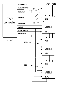
FIG. 1 shows the prior art general architecture of an IC which contains 1149.4
test
access circuitry;
FIG. 2 illustrates a schematic of prior art analog boundary module circuitry;
FIG. 3 illustrates the TAP controller state diagram specified by both the
1149.1 and
1149.4 standards;
FIG. 4 is a schematic of circuitry that prevents captures during the CaptureDR
state
of the TAP controller connected to ABMs, according to a first embodiment of
the present invention, the circuitry including Digital Boundary Cells, DBC,
and
scan cells, SC;
FIG. 5 is a schematic of a prior art digital boundary cell (DBC);
FIG. 6 is a schematic of a prior art non-boundary scan cell (SC);
FIG. 7 shows waveforms for the circuit shown in FIG. 6;
FIG. 8 is a schematic of circuitry, similar to FIG. 4, that prevents captures
during the
CaptureDR state of the TAP controller connected to ABMs, according to a
first embodiment of the present invention;
FIG. 9 is a schematic of circuitry, similar to FIG. 8, but which additionally
generates a
second UpdateDR signal, according to a second embodiment of the present
invention
FIG. 10 is a schematic of an ABM that has two UpdateDR control inputs
according to
an embodiment of the present invention;
FIG. 11 illustrates waveforms for the circuit shown in FIG. 9 and FIG. 10;
FIG. 12 shows a schematic of circuitry that generates a FuIlUpdate signal to
control
whether the ABMs update all register bits or only a subset of register bits,
according to a third embodiment of the present invention; and
FIG. 13 is a circuit schematic of an ABM having a control input for disabling
updates
for two latches, according to an embodiment of the present invention.
CA 02329597 2000-12-22
-6-
Detailed Description
In the following detailed description, numerous specific details are set forth
in
order to provide a thorough understanding of the present invention. However,
it will
be understood by those skilled in the art that the present invention may be
practiced
without these specific details. In other instances, well known methods,
procedures,
components and circuits have not been described in detail so as not to obscure
aspects of the present invention.
Before describing the various embodiments of the present invention, it would
be useful to describe IC 10 in more detail with reference to FIG. 1, 2 and 3.
As
previously mentioned, the circuit includes a TAP controller 12. The controller
includes a clock input TCK, a Test Mode Select Input, TMS, for sequencing the
controller through the 16 states shown in FIG. 3. The controller also includes
a Test
Data Input, TDI, for loading (or "shifting" or "scanning") logic values into
the IC and a
Test Data Output, TDO, for unloading data out of the IC. The IC further
includes
internal analog circuits 80 and internal digital circuits 82. The analog
circuitry is
connected to circuit nodes or pins 18 via analog boundary modules 84. The
digital
circuits are connected to circuit nodes or pins 86 via analog boundary modules
or
boundary modules 88. A pair of busses AB1 and AB2 connect each of analog
boundary modules 84 and 88 to test bus interface circuit 26 and are used to
monitor
or drive circuit nodes according to the IEEE 1149.4 standard.
The analog boundary modules are illustrated in FIG. 2 and were described
earlier. It will be noted that shift register elements 64, 66, 68 and 70 are
serially
connected between a module Scan Data Input, SDI, and a Scan Data Output SDO,
which are serially connected to other modules along previously mentioned scan
path
40. The ShiftDR signal output by the TAP is connected to multiplexer 60 and
serves
to configure shift register elements 64, 66, 68 and 70 in a shift or scan mode
when
active and in a capture mode when inactive. Update latches 42, 44, 74 and 76
are
associated with shift register elements 64, 66, 68 and 70, respectively, and
are
controlled by TAP controller UpdateDR output signal. Analog switches 22 and 24
are controlled by a mode signal, Mode2, output by the TAP and the logic values
in
update latches 44 and 42, respectively. The switches are enabled by loading a
switch enabling bit, logic 1, into their associated update latches. The
circuit further
includes 3-state digital driver 90, which is enabled by a logic 1 applied to
its control
input.
CA 02329597 2000-12-22
The present invention seeks to provide a method and circuit for performing a
fast sequential access of the circuit pins of one or more ICs. The various
embodiments of the present invention will now be described. FIG. 4 and FIG. 8
are
similar to one another except that FIG. 4 includes a combination of analog
boundary
modules 98, digital boundary cells 100 and scan cells 102 while FIG. 8
includes only
analog boundary modules 120. As shown, TAP controller 12 is provided with
output
CIockDR, which is applied to the clock input of shift register elements in the
Boundary Modules, including ABMs, DBCs, and SCs; UpdateDR which is applied to
the clock input of update latches; ShiftDR which is applied to the
multiplexers used
to configure shift register elements in shift mode or capture mode, and one or
more
mode signals, which are used for various purposes not relevant to the present
invention. The controller also includes a ScanDataOut output and a ScanDataln
input connected to the previously mentioned SDI and SDO terminals of ABMs, and
DBCs.
In accordance with one aspect of the present invention, there is provided a
circuit 104 which facilitates fast sequential access to the circuit nodes. The
circuit
uses additional signals output by the TAP controller, including a
CaptureDRState
signal and a NoCapture signal.
The CaptureDRState signal and NoCapture signals are applied to respective
inputs of a NAND gate 112 whose output is applied to one input of an AND gate
114
which gates the CIockDR signal (waveform 74w in FIG. 7) and outputs a CIockDRa
signal 76w. The other input of AND gate 114 is logic 0 only when the
CaptureDRState signal output indicates the TAP controller is in CaptureDR
state 58
and the NoCapture output indicates the TAP controller is in a "Rapid Access"
mode.
By preventing the CIockDR signal from propagating to the DBCs 100 and to the
internal SCs, 102, as shown by waveform 76aw, the normal capture function is
suppressed. Waveform 76w shows the common CIockDR signal during normal
operation, when the NoCapture signal is logic 0. Waveform 76aw shows the
signal
during the "Rapid Access" mode, when the NoCapture signal is logic 1.
DBCs 100 illustrated in FIG. 4 may be configured as shown in FIG. 5 which
illustrates a shift register element 106, an associated update latch 108, and
a first
multiplexer 110 and a second multiplexer 112. The ShiftDR controller output is
applied to the select input of multiplexer 110. The output of shift element
106 is
connected to the update latch input and to the cell SDO output. DBC output 115
is
CA 02329597 2000-12-22
_g_
fed back and applied to the "0" input of multiplexer 110. The SDI input is
applied to
the "1" input of multiplexer 110. A DBC input 116 is applied to the "0" input
of
multiplexer 112. The output of latch 108 is applied to the "1" input of
multiplexer 112.
A mode signal is applied to the select input of multiplexer 112. When ShiftDR
is
logic 1, the DBC is configured in "shift mode" in which all of the boundary
modules
which comprise the BSR are connected in series for loading or unloading logic
values to and from the boundary modules. When ShiftDR is logic 0, the cell is
configured in "capture mode" in which the DBC output is applied to the input
of the
shift register element. A capture operation occurs when a transition occurs on
clock
signal CIockDR at the clock input of the shift register element. It is this
operation
which causes "data corruption" as it relates to performing sequential circuit
node
accesses. The same applies to the ABM circuits.
Internal scan cells 102 may be configured as shown in FIG. 6. The scan cell
includes a shift register element 118 clocked by CIockDR and a multiplexer 119
which is controlled by ShiftDR.
FIG. 8 contains the same circuit 104 as shown in FIG. 4. However, in this
circuit all of the boundary cells are ABMs 120 as shown in FIG. 2, containing
two
shift register elements 68 and 70 which control digital functions and two
shift register
elements 64 and 66 that control analog switches. The enable pin 122 of the
digital
driver 90 is designed such that the driver is enabled by a logic 1. The analog
switches are designed such that each is enabled by a logic 1 in the
corresponding
register bit.
Returning to circuit 104, the NoCapture signal can be set either by loading an
instruction that sets an Instruction Register bit, or by loading a data
register bit, or by
loading into an additional bit of the BSR. The CaptureDRState signal is
typically
available in the 1149.1/1149.4 standard TAP controller. The instruction puts
the IC
and TAP controller into a "Rapid Access" mode which prevents corruption of
data in
internal data registers when the controller is sequenced through the CaptureDR
state
to access the ShiftDR state (see FIG. 3).
In accordance with the method of the present invention, there are two basic
steps to perform a fast sequential access of a plurality of circuit nodes or
pins on the
chip. The first step is an initialization step which involves scanning logic
values into
the serially connected shift register elements of the boundary modules and
then
loading the logic values into the update latches associated with the shift
register
CA 02329597 2000-12-22
_g_
elements. The logic values include at least one switch enabling value for
enabling at
least one analog switch associated with a first circuit node to be accessed.
In the
embodiments of FIG. 4 and FIG. 8, the logic values are logic 0 except for the
switch
enabling value which is a logic 1. In other embodiments described later, logic
values
other than logic 0 may be loaded for non-switch control shift register
elements.
Upon completion of the initialization step, the first circuit node may be
accessed by
either monitoring or driving it. Prior to beginning the second step, the
NoCapture
signal is activated and remains active for the balance of the procedure.
The second step simply comprises, for each subsequent circuit node to be
accessed, shifting the switch enabling logic value from one boundary module to
the
next, updating the latches associated with analog switches which control the
circuit
node, and accessing the subsequent circuit node. This step is repeated as many
times as necessary to access all of the circuit nodes.
In the conventional method, it is necessary to initialize the boundary
register
each time a circuit pin is accessed. This is necessary because the
conventional
method permits the normal capture operation to occur when the controller is
sequenced through its various states and, therefore, the data is corrupted, in
the
manner explained above in the description of FIG. 5 and cannot be re-used for
accessing additional circuit nodes. It will be seen that, if a BSR comprises N
bits,
N+4 clock cycles will be required each time a pin is accessed, as explained in
detail
earlier. The additional four clock cycles are associated with sequencing of
the
controller to the necessary states for loading and updating data. In contrast,
the
present invention only requires the same additional four clock cycles plus the
clock
cycles required to advance the switch enabling logic value from one boundary
module to the next, which for an ABM would be four clock cycles for a total of
eight
clock cycles. The BSR data is not corrupted because the capture operation is
suppressed. The number will vary depending on how far it is necessary to
advance
the switch enabling bit. In a circuit having only ABMs of identical
construction, the
number of logic 0's scanned in in sub-step 5 above would be four, assuming the
switch enabling bit is shifting to a corresponding shift register element in
the next
ABM. The number of logic 0's is one if the next switch in sequence is located
in the
current ABM. The number of logic 0's is three if the next switch in sequence
is the
first switch in the next ABM.
The following is a more technical description of the second step of the
present invention. With the NoCapture signal inactive (Logic 0), the
controller is
CA 02329597 2000-12-22
-10-
sequenced to the ShiftDR state and then an appropriate number of clock cycles
are
applied to scan in logic values into the TDI input of the IC. When these logic
values
have been fully loaded, the controller is sequenced to the CIockDR state,
which
activates the CIockDR signal and updates all update latches and enables the
switch
of interest. The circuit node may no~nr be monitored or driven.
With the NoCapture signal active, the CIockDR signal is suppressed as the
controller is sequenced through the CaptureDR state. Therefore, even though
the
ShiftDR signal is inactive, which configures the shift register elements in
capture
mode, the scan modules are unable to perform a capture operation without the
clock
input. The active NoCapture signal does not affect the shift or scan operation
because CIockDR is only disabled during the CaptureDR state.
With reference to the state diagram of FIG. 3, the second basic step of the
method comprises the following specific steps: 1. while TMS=1, toggle TCK to
proceed from the Run-test/Idle state, the Update-DR state or the Update-IR
state to
the Select-DR-Scan state; 2 while TMS=0, toggle TCK to proceed from the
Select-DR-Scan state to the Capture-DR state, (in which capture is
suppressed); 3.
while TMS=0, toggle TCK to proceed from the Capture-DR state to the Shift-DR
state; 4. while TMS=0, repeatedly toggle TCK to scan in just enough logic
zeroes to
shift bits to next ABM; 5. while TMS=1, toggle TCK to proceed from the Shift-
DR
state to the Exit1-DR state; and 6. While TMS=1, toggle TCK to proceed from
the
Exit1-DR state to the Update-DR state, which updates all latches to output new
bit
values.
The invention also contemplates enabling two analog switches at a time. To
that end, in the initialization step, a pair of sequential logic 1 switch
enabling bits are
scanned in. This pair of bits is then shifted from one ABM to the next with
each
sequential circuit node access.
The circuits illustrated in FIG. 4 and FIG. 8 provide the advantage that they
may be used without modification of conventional boundary modules (ABMs, DBCs)
but do not allow including specific digital driver logic values (unless such
values are
logic 0's) during the BSR initialization step because such values would be
replaced
during each of the second and later scan and update operations. The
embodiments
of FIG. 9-13 may be used when it is desired to load non-zero logic values and
have
those values remain active, without corruption, throughout all sequential
circuit pin
accesses. These embodiments suppress capture as in FIGS. 4 and 8, but
additionally provide a mechanism for selectively updating different groups of
update
CA 02329597 2000-12-22
-11-
latches at different times. More specifically, these embodiments provide
mechanisms for updating switch-associated update latches separately from
latches
which do not control analog switches.
The embodiment of FIG. 9 uses the same circuit 104 illustrated and
described with reference to FIG. 4 and FIG. 8. Accordingly, the same reference
numerals are used to designate the same parts. However, this circuit uses the
normal UpdateDR signal to control update latches that control analog switches
and
generates a second UpdateDR signal for controlling update latches that do not
control analog switches. The second signal is generated by a circuit 130 and
is
derived by gating first Update signal with the NoCapture signal by means of
AND
gate 132. AND gate 132 receives the inverted NoCapture signal and the UpdateDR
signal and outputs a second UpdateDR signal, labelled, UpdateDRa. When the
NoCapture output is in its initial reset state, logic 0, UpdateDRa is the same
as the
UpdateDR signal as shown by the waveforms 77w and 121w in FIG. 11. When the
NoCapture output is set, the UpdateDRa output is set to a constant logic value
independent of the UpdateDR signal, as shown by waveform 121aw of FIG. 11.
DBCs and SCs could also be connected in the scan path of FIG. 4 and FIG 8
without
affecting the sequence described for the present invention.
The addition of circuit 130 allows modification of the first and second method
steps described earlier. In the first method step, logic values other than
logic 0's and
the switch enabling value may loaded. Thus, digital driver enabling values and
any
such values may be included without concern that these values will be
corrupted
during execution of the method. In addition, the first method step is modified
by
performing two update operations simultaneously in order to (a) update all
latches
which control analog switches and (b) update all other update latches.
The second method step of the present invention is modified by restricting its
update operation to updating only update latches associated with analog
switches.
This requires a minor modification to the ABMs, as shown in FIG. 10.
FIG. 10 illustrates an ABM adapted to use the second UpdateDR signal. The
circuit is substantially the same as the previously described ABM circuit
(FIG. 2) and,
accordingly the same reference numerals have been used to designate the same
parts. It will be noted that UpdateDRa is connected to the clock input of each
of
update latches 74 and 76 while the UpdateDR signal is connected to the clock
input
of each of update latches 42 and 44, which control analog switches 24 and 22,
respectively.
CA 02329597 2000-12-22
-12-
FIG. 12 provides an alternative arrangement for updating two groups of
update latches independently. In this case, circuit 130 provides an inverter
134
which receives the NoCapture output and generates an output, labelled
FuIlUpdate,
which is applied to each of the ABMs. Referring to FIG. 13, which illustrates
an
ABM especially adapted for use with the circuit of FIG. 12, it will be seen
that
FuIlUpdate is applied to one input of an AND gate 136. The other input to the
AND
gate is the UpdateDR signal. The output of AND gate 136 is applied to the
clock
inputs of update latches 74 and 76. This embodiment would be particularly
useful in
situations where locally generated signals are desired as compared to the
centrally
generated signals provided by the previous embodiment.
The method used with the embodiment of FIG. 12 is the same as that of
FIG. 9. The same method can be used for a plurality of chips on a circuit
board. In
that situation, the boundary scan registers of two or more ICs are serially
connected
to define one large shift register. The method of the present invention can
then be
used to sequentially access the circuit nodes of all ICs in one sequence.
In summary, the circuits described and shown in FIG. 4 - FIG. 13 facilitate
fast analog access to a plurality of pins on an IC, with as few as eight TCK
clock
cycles between each access, independent of the number of pins on the IC. For
an
IC with P pins, as described in the Introduction, N = 4P + 4 bits are needed
to load
the BSR, hence this number of bits must be loaded to provide analog access to
the
first pin. For P>100, N is approximately equal to 4P.
To access each subsequent pin, eight clock cycles are needed. The total
time per measurement is therefore:
4P~fTCK +P(TMeasure + 8~fTCK ) = P(TMeasure + 12/fTCK )
which is linearly proportional to the number of pins.
The total time to measure/apply 6 voltages for an IC with P pins is:
6P(TMeasure + 12/fTCK )
For an IC with 100 signal pins, fTCK=10 MHz, and TMeasure = 10 Ns, the test
time
would be approximately 6.7 ms, and the number of test vectors would be 67,000.
For an IC with 1000 signal pins and fTCK =10 MHz, the test time would be
approximately 61.2 ms, and the number of test vectors would be 612,000.
Compared with the 2.7 seconds required for conventional method, these test
times
are between 4 and 40 times faster than the boundary scan-based prior art
described
herein, and comparable to prior art tests that directly access all pins of an
IC.
CA 02329597 2000-12-22
-13-
Although the present invention has been described in detail with regard to
preferred embodiments and drawings of the invention, it will be apparent to
those
skilled in the art that various adaptions, modifications and alterations may
be
accomplished with departing from the spirit and scope of the present
invention.
Accordingly, it is to be understood that the accompanying drawings as set
forth
hereinabove are not intended to limit the breadth of the present invention,
which
should be inferred only from the following claims and their appropriately
construed
legal equivalents.