Note: Descriptions are shown in the official language in which they were submitted.
CA 02329677 2000-12-27
v_i
HIGH SPEED CARD ED E CONNECTORS
BACKGROUND OF THE INVENTION
1. Field of the Invention
The present invention relates to modular electrical connectors and, more
particularly, to card edge connectors with shielded modular inserts.
2. Discussion of Earlier Developments
There is a plethora today of known constructions of multiple contact
electrical connectors providing a variety of features including some form of
modular construction and signal shielding. A few of the more pertinent
patented constructions known to the applicants will now be briefly
described.
U.S. Patents, No. 4,067,637 to Narozny, No. 4,324,451 to Ammon et al.
and 4,530,561 to Tyree et al. are generally descriptive of currently used
card edge connectors.
U.S. Patent No. 4,550,959 to Grabbe et al. discloses an expandable,
modular card edge connector in which individual elements are unified into
a longitudinal whole by melting an interfacing material between adjoining
sections. Withdrawal of the heat source results in a generally rigid
assembly.
U.S. Patent No. 4,586,254 to Ammon et al. discloses a modular printed
circuit card edge connector in which two end bodies engage opposite ends
of a single insulator body which contains the entire population of contacts.
It is intended to be manufactured in a generally long bar, or by a
continuous molding process, to provide for cutting to length a single,
unitary housing component containing the desired number of contact
arrays.
CA 02329677 2000-12-27
2
U.S. Patents, No. 5,013,263 to Gordon et al. and No. 5,584,728, both
disclose an electrical connector built up of interlocking modules.
Specifically, the connector structures have conversely shaped interlocking
parts at their ends to interlock end-to-end with similar structures to form
a substantially self supporting structure that can have any desired
number of contacts, each spaced an integral multiple of the same unit
distance from all of the contacts on all of the modules.
U.S. Patent No. 5,104,341 to Gilissen et al. discloses an electrical
connector mountable to a printed circuit board which includes a plurality
of insulated housings. The housings accept a plurality of terminal
subassemblies into which a plurality of electrical terminals are integrally
molded. Shield members are insertable into the rear of the connector
housing to shield adjacent vertical rows of terminals from cross talk.
U.S. Patent No. 5,704,793 to Stokoe et al. discloses an electrical connector
which is scalable in its engagement widths, but not by means of
combinations of contact modules. The scalable components of this
invention are contained within a longitudinal latching and clamping
mechanism. This invention uses a single and discrete membrane such as a
flex circuit, which must be clamped on to the card edge pattern by the
latching and clamping mechanism.
U.S. Patent No. 5,716,237 to Conorich et al. discloses an electrical
connector which compensates from near-end cross talk at its mating
section with near-end cross talk of an opposite polarity and essentially
equal magnitude. Conductive plates connected to the conductors of the
connector provide capacitive coupling unbalance between the adjacent
pairs of conductors to produce the necessary opposite polarity, equal
magnitude, near-end cross talk.
CA 02329677 2000-12-27
~.....-;
3
SUMMARY OF THE INVENTION
The present invention relates, generally, to a card edge connector which
includes an elongated longitudinally extending outer frame defining a
reception region. The electrical connector is adapted to receive a plurality
of chiclet modules including contact members lying in parallel laterally
extending planes which, as an assembly, are positioned to connectively
engage with mating contacts. Each chiclet module includes an insulative
housing having first and second spaced generally parallel elongated
passages therein and a card receiving recess for reception therein between
the first and second passages of a planar card having opposed surfaces
with conductive contact members thereon. First and second elongated
contacts are firmly received, respectively, in the first and second passages.
Each has a first contact surface positioned, respectively, for engagement
with first and second of the mating contacts. The card receiving recesses of
the chiclet modules as a group define a longitudinally extending card
receiving slot. The elongated contacts each include a second contact
surface projecting into the card receiving slot for engagement,
respectively, with second conductive contact members on the planar card.
A tubular ground shield may be slidably received on the insulative
housing in proximate engagement with its outer peripheral surface. In
this instance, the ground shield includes a first integral ground contact for
engagement with a ground contact of an external unit associated with the
mating contacts engaged by the first contact surfaces of the first and
second elongated contacts and a second integral ground contact for
engagement with a ground contact surface on the planar card inserted into
the card receiving slot.
A chiclet module may be described as a pre-assembled module which
includes one or more contacts, an insulator, and one or more shields. The
pre-assembly of identical modules creates an advantageous economy of
scale. Modular chiclet designs can be easily built or altered to afford
CA 02329677 2000-12-27
4
interconnection of the exact number of contacts desired, relieving the user
of having to select an oversized connector.
Each chiclet module can independently mate to a designated pattern of
pads positioned along a substrate edge. The substrate may be either a
printed circuit card or any other embodiment of contacts residing along an
edge of a thin insulator membrane or flat plane. One or more series of
chiclet modules may be held in specific alignment by means of their
emplacement in groups, gangs, or arrays residing in an overall plastic or
metal frame.
Alignment for mating a stacked series of chiclet assemblies with a series of
known target objects, such as a 2-dimensional contact pad pattern,
normally presents a challenge of tolerance stack-up of the individual
assemblies; the positional error of the last assembly in a series is
perturbed by the sum, or accumulated tolerances, of all of the elements
between it and the known position of a datum or reference object such as
an alignment structure. The present invention advantageously eliminates
accumulated tolerance by providing positioning structures in the overall
frame for each chiclet module.
The present invention entails an insulator chiclet module whose interior
contacts are shielded to the maximum extent by one or more generally
box-shaped or tube-shaped shields enveloping as completely as possible
the plastic insulator and its internal contacts. These shields comprise a
part of the chiclet module subassembly proper, and no other insulating,
shielding, or grounding structures are required in the overall frame.
Manufacture of the shields into their closed or nearly closed perimeter
cross sections may proceed from seamless or extruded tubes or from flat
sheet stock folded into box-like or tube-like structures. A single shield may
envelop the entire insulator structure and the contacts contained within,
or an insulator may be provided with two or more contact-isolating lobes
CA 02329677 2000-12-27
and a set of shields of which envelop individual lobes as completely as
possible. In this card edge embodiment, the insulator is bilaterally
symmetrical about the midplane of the card it admits, and this insulator
accepts two box-like shields, one on each side of the card midplane. The
5 shields include their own contacts members, and either these or their
designated pads on the card edges, or both, may be specially elongated or
positioned so as to establish, in a pre-emptive manner, shielding or
common electrical grounding across the contact interface, in advance of
electrical interconnection of other sensitive signal lines.
In some cases, mutual electrical contact between the shields of
neighboring contacts is preferred, and the invention provides for chiclet
modules with spring tabs or fingers which contact neighboring chiclet
modules. In cases where individual electrical potentials of neighboring
shields are to be maintained separate, these neighboring contacts may be
eliminated, or an insulating structure may be provided in the overall
frame to interpose or defeat this shield-to-shield interconnection.
The chiclet modules of the invention are designed to provide electrical
contact preferably to both sides of the engaged or inserted substrate, card,
or membrane edge. Single-sided deployments are also within the scope of
the invention.
The inventive device may engage pad patterns of uniform spacing or pitch,
or of a repeated or a staggered series of non-uniform patterns, as is
common with contact arrays of shielded differential signal pairs.
Individual chiclet modules, including those which span several units of
pad pattern pitch, may be provided which engage with locally unique
patterns. An example of this case would be an assembled connector
comprising a first series of shielded differential pair units with repeated
patterns of contacts on a first pitch, a second series of non-shielded
modules each of which present a gang of conventional contact pairs on a
CA 02329677 2000-12-27
I~w'
6
second pitch, and a third series of high current power modules comprising
heavy-duty contacts on a third pitch.
Thus is described an assembly containing sub-assemblies of unspecified
numbers of identical shielded, modular units, which may be interspersed
with non-shielded units of lower cost and also special-purpose units such
as those designed for high current interconnections. The invention
provides an overall frame to precisely position these modules with no
accumulated tolerance stack-up. Unit members of the pattern of
positioning structures provided in the frame may individually accept
modules of a unitary design, or as a group may accept larger modules
spanning several of these positioning structures. If desired, one or more
positions in this frame may be left empty, or a blank or dummy module
may be provided. The pitches and patterns of the contacts residing within
these modules are neither necessarily equal to nor necessarily related to
the pitch and pattern of the positioning structures in the overall frame.
Simple card-edge connectors rely on one or both end walls of the connector
to align it with the pad patterns residing on the card. It is also known that
one or more intermediate notches may be provided along a card edge for
polarity, identification, and for improved registration of the connector to
the pad patterns on the card by means of including a plenum or stub in
the connector which registers in the slots) under proper insertion. While
it is possible to provide special-purpose chiclet modules each of which
include local registration features, the cost of producing a series of
complimentary mating features along the card edge is likely to prohibit
this approach. Therefore, our invention preferably provides a primary
alignment plenum or stub or a primary set of these, incorporated in the
overall frame in a manner which defines a precise positional relationship
between this alignment feature or feature set, and the series of positioning
structures within the overall frame which align the chiclet module sets.
These primary features in the overall frame provide initial and precise
CA 02329677 2000-12-27
alignment of the chiclet modules to their associated patterns on the card
edge, by means of the chiclet modules being engaged and registered by the
series of positioning structures in the overall frame and by virtue of the
fact that both the positioning structures and the primary alignment
features are integral features of the overall frame. Therefore, the
locational accuracy of the chiclet modules with respect to an alignment
slot provided in the card edge (complimentary to the primary alignment
feature of the frame) accrues no accumulated tolerances associated with
the number, type, or distance from the frame's primary alignment features
to its positioning structures which locate the chiclet modules. By this
arrangement, the locational accuracy of any particular chiclet module is
limited only by the accuracy and reliability of the process used to provide
the features of the overall frame.
While conventional housings designed to receive a series of modules often
provide an individual aperture or receiving section for each individual
module or insert, our overall frame provides one or a small series of large
longitudinal openings each of which may accept our chiclet modules in
groups. The positioning structures mentioned elsewhere reside nearby and
extend within the general openings. Our chiclet' modules are designed
with complimentary features to accept precise alignment by these
positioning features in the frame. According to the preferred embodiment,
these features are common to all types of chiclet modules and all openings
in the frame, which affords a maximum diversity of the combinations and
compositions of groups of chiclet modules available for assembly into the
overall frame. However, it is understood that sets of frames and chiclet
modules may be designed with distinct families of positioning structures
and features, whereby these frames, in offering a first set of positioning
structures in any one aperture and a mechanically incompatible second
and distinct series of positioning structures in any other aperture will
prevent the mingling of one family of chiclet module designs with a second
family of designs within the same aperture. This segregation may be
..
CA 02329677 2000-12-27
8
advantageous as a polarity feature, or as a means of eliminating assembly
operator error, or to provide a special and proprietary series of product
distinct from a general commodity design. An additional advantage of such
segregation is the separation and deliberate location of a distinct series of
chiclet modules of an especially robust design capable of withstanding
severe service, such as high voltages, high currents, or exceptional mating
life demands, whose special positioning structures are mechanically
incompatible with elements from the series of standard service designs. In
this case, such segregation can advantageously prevent an undesirable or
dangerous condition, including the untimely or catastrophic failure of an
improperly positioned standard service unit or chiclet module group
accidentally subjected to severe service.
Where a continuous wall or perimeter structure would occlude visual
inspection of good manufacturing processes, such as successful solder
reflow of surface mount contacts, or full and complete insertion of chiclet
modules into the overall frame, the frame is preferably provided with
apertures, or continuous longitudinal cut-away sections, or a pattern of
cut-out profiles (e.g., perforated, invected, embattled, engrailed, etc.)
affording such visual inspection by completely or intermittently revealing
internal features, component positions, or the results of operations
otherwise enclosed by the overall frame.
A primary feature, then, of the present invention is the provision of a
modular electrical connector.
Another feature of the present invention is the provision of such a modular
electrical connector in the form of a card edge connector with shielded
modular inserts.
Still another feature of the present invention is the provision of such a
modular connector including an elongated longitudinally extending outer
frame defining a reception region adapted to receive a plurality of chiclet
CA 02329677 2000-12-27
--
9
modules including contact members and lying in parallel laterally
extending planes which, as an assembly, are positioned to connectively
engage with mating contacts.
Yet another feature of the present invention is the provision of such a
modular connector wherein each chiclet module includes an insulative
housing having first and second spaced generally parallel elongated
passages therein and a card receiving recess for reception therein between
the first and second passages of a planar card having opposed surfaces
with conductive contact members thereon, a first elongated contact firmly
received in the first passage having a first contact surface positioned for
engagement with a first of the mating contacts, a second elongated contact
firmly received in the second passage having a first contact surface
positioned for engagement with a second of the mating contacts, wherein
the card receiving recesses of the plurality of chiclet modules as a group
defines a longitudinally extending card receiving slot, the first elongated
contact including a second contact surface projecting into the card
receiving slot for engagement with a first conductive contact member on
the planar card inserted into the card receiving slot and the second
elongated contact including a second contact surface projecting into the
card receiving slot in the direction of the first elongated contact for
engagement with a second conductive contact member on the planar card
inserted into the card receiving slot.
Still a further feature of the present invention is the provision of such a
modular connector wherein a tubular ground shield is slidably received on
the insulative housing in proximate engagement with its outer peripheral
surface, the ground shield including a first integral ground contact for
engagement with a ground contact of an external unit associated with the
mating contacts engaged by the first contact surfaces of the first and
second elongated contacts and a second integral ground contact for
CA 02329677 2000-12-27
engagement with a ground contact surface on the planar card inserted into
the card receiving slot.
Still another feature of the present invention is the provision of such a
5 modular connector including first and second ground shields, each having
a C-shaped cross section, slidably received, respectively, on the insulative
housing in opposed relationship and in proximate engagement with its
outer peripheral surface, the first ground shield generally overlying the
first elongated passage, the second ground shield generally overlying the
10 second elongated passage, the first ground shield having first and second
opposed limbs proximately overlying the first and second major sides,
respectively, a first side limb proximately overlying the first minor side,
and a first flange limb extending transverse of the first opposed limb
slidably received in the first elongated slot whereby the first ground shield
substantially completely surrounds the first elongated contact received in
the first passage, the second ground shield having third and fourth
opposed limbs proximately overlying the third and fourth major sides,
respectively, a second side limb proximately overlying the second minor
side, and a second flange limb extending transverse of the third opposed
limb slidably received in the first elongated slot whereby the second
ground shield substantially completely surrounds the second elongated
contact received in the second passage, the first and second ground shields
both including a first integral ground contact for engagement with a
ground contact of an external unit associated with the mating contacts
engaged by the first contact surfaces of the first and second elongated
contacts, each of the first and second ground shields including a second
integral ground contact for engagement with an associated ground contact
surface on the planar card inserted into the caxd receiving slot.
Other and further features, advantages, and benefits of the invention will
become apparent in the following description taken in conjunction with
the following drawings. It is to be understood that the foregoing general
CA 02329677 2000-12-27
~-:
' 11
description and the following detailed description are exemplary and
explanatory but are not to be restrictive of the invention. The
accompanying drawings which are incorporated in and constitute a part of
this invention, illustrate one of the embodiments of the invention, and
together with the description, serve to explain the principles of the
invention in general terms. Like numerals refer to like parts throughout
the disclosure.
BRIEF DESCRIPTION OF THE DRAWINGS
The foregoing aspects and other features of the present invention are
explained in the following description, taken in connection with the
accompanying drawings, wherein:
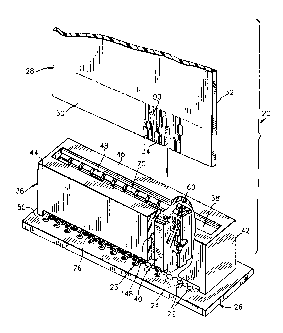
Fig. 1 is an exploded perspective view of a card edge connector assembly
embodying the present invention.
Fig. 2 is a side elevation view of the card edge connector assembly
illustrated in Fig. 1, certain parts being cut away and shown in section;
Fig. 3 is a top plan view of the card edge connector assembly illustrated in
Figs. 1 and 2;
Fig. 4 is an end elevation view of the card edge connector assembly
illustrated in Figs. 1, 2, and 3;
Fig. 5 is a perspective view of a grouping of chiclet modules according to
the invention positioned on a motherboard but absent the outer frame
which normally envelops the chiclet modules;
Fig G is a perspective view of an insulative housing for a chiclet module
with elongated contacts in place;
CA 02329677 2000-12-27
12
Fig. 7 is another perspective view of the insulative housing for a chiclet
module but without elongated contacts being illustrated;
Fig. 8A is a front elevation view of the insulative housing illustrated in
Figs. G and 7;
Fig. 8B is a side elevation view of the insulative housing illustrated in
Figs. 6, 7, and 8A;
Fig. 8C is a rear elevation view of the insulative housing illustrated in
Figs. G, 7, 8A, and 8B;
Fig. 8D is a side elevation view, taken opposite that of Fig. 8B of the
insulative housing illustrated in Figs. 6, 7, 8A, 8B, and 8C;
Fig. 9 is a perspective view illustrating opposed ground shields, each
having a C-shaped cross section for slidable reception, respectively, on an
outer peripheral surface of the insulative housing of Figs. G, 7, 8A, 8B, 8C,
and 8D;
Fig. 10 is a front elevation view of a chiclet module into which a planar
card such as a daughter board is about to be inserted;
Fig. 11 is a side elevation view of the chiclet module illustrated in Fig. 10
Fig. 12 is a perspective view illustrating a single tubular ground shield
which is another embodiment of the pair of opposed ground shields
illustrated in Fig. 9;
Fig. 13 is side elevation view of a modified chiclet module which includes
the single tubular ground shield illustrated in Fig. 12;
Fig. 14 is a detail view in section illustrating a portion of the outer frame
provided with a variety of locating features at a plurality of longitudinally
spaced locations for positioning the chiclet modules at defined spaced
locations within the outer frame;
CA 02329677 2000-12-27
13
Figs. 15, 1G, 17, 18, are detail section views, similar to Fig. 14,
illustrating
variations of the construction of Fig. 14, each illustrating a portion of the
outer frame provided with a variety of different locating features , at a
plurality of longitudinally spaced locations, also for positioning the chiclet
modules at defined spaced locations within the outer frame;
Fig. 19 is a detail exploded view in elevation illustrating a modified outer
frame in which a pair of longitudinally spaced septum members are
provided, each with a registration feature enabling a suitably formed
planar card with conductive contact members to be fully inserted into the
card receiving slot of the card edge connector assembly.
DETAILED DESCRIPTION OF THE PREFERRED EMBODIMENT
Referring to Fig. 1, there is shown an exploded perspective view of a card
edge connector assembly 20 incorporating features of the present
invention. Although the present invention will be described with
reference to the embodiments shown in the drawings, it should be
understood that the present invention can be embodied in many alternate
forms of embodiments. In addition, any suitable size, shape or type of
elements or materials could be used.
The card edge connector assembly 20 includes a plurality of contact pads
22 arranged in a contact pattern 23 on an underlying contact surface 24 in
the form of a motherboard 2G, for example. A planar card 28, a daughter
board, for example, has first and second opposed surfaces 30, 32 with
conductive contact members 34 on at least one of the opposed surfaces.
Viewing now also Figs. 2-5, an elongated longitudinally extending outer
frame 3G defines a reception region 38 which is adapted to receive a
plurality of chiclet modules 40. Each of the chiclet modules 40 includes
contact members (to be described below) and the chiclet modules lie side
by side in parallel laterally extending planes which, as an assembly, are
CA 02329677 2000-12-27
~J
14
positioned to connectively engage with the mating contact pads 22 on the
underlying contact surface 24. The outex frame 36 includes opposed
spaced end walls 42, opposed spaced side walls 44, and a top wall 46
integrally joining the end walls and the side walls. The end walls, side
walls, and top wall together define the reception region 38, the top wall
having a longitudinally extending aperture 48. The end walls 42 and the
side walls 44 extend to a lower rim 50 distant from the top wall 4G and
define, interiorly, an opening 52 through which the chiclet modules are
inserted into the reception region 38.
Turning now to Figs. G, 7, and 8A-8D, each chiclet module 40 includes an
insulative housing 54 which has first and second spaced generally parallel
elongated passages 5G, 58 therein and a card receiving recess GO for
reception of the planar card 28 (Fig. 1) between the first and second
passages. A first elongated contact 62 is firmly received in a known
manner in the first passage 5G and has a first contact surface G4
positioned for engagement with an associated contact pad 22 (Fig. 1) on
the contact pattern 23 of the underlying contact surface 24 using known
techniques. In a similar fashion, a second elongated contact 6G is firmly
received in the second passage 58 having a first contact surface G8
positioned for engagement with another associated contact pad 22 on the
contact pattern 23 of the underlying contact surface 24. Although shown
as being surface mount contacts, any type of termination (e.g. press-fit,
pin-in-paste) could be used.
As seen in Fig. 1, the card receiving recesses GO of the plurality of chiclet
modules 40 integrated as a group within the outer frame 3G define a
longitudinally extending card receiving slot 70. Turning back to Fig. G,
the first elongated contact G2 includes a second contact surface 72
projecting into the card receiving slot 70 (or recess 60 of an individual
chiclet module 40). The second contact surface 72 engages with an
associated conductive contact member 34 on the first surface 30 of the
CA 02329677 2000-12-27
' planar card 28 inserted into the card receiving slot. In a similar fashion,
the second elongated contact 66 includes a second contact surface 74
projecting into the card receiving slot 70 (or recess 60 of an individual
chiclet module 40) in the direction of the first elongated contact 62.. This
5 time, the second contact surface 74 engages with a second one of the
conductive contact members 34, this one being on the second surface 32 of
the planar card 28 inserted into the card receiving slot.
With continued attention to Fig. 1, the lower rim 50 of the outer frame 36
10 includes a cutout region 7G enabling visual inspection of the first contact
surfaces G4, G8 of the first and second elongated contacts G2, GG when
engaged with their associated contact pads, respectively. Also, aperture
48 of the outer frame 3G is aligned with the card receiving slot 70 when
the plurality of chiclet modules are received in the reception region 38.
Turn now to Figs. 9, 10, and 11 which illustrate opposed ground shields
78, 80, each having a C-shaped cross section for slidable reception,
respectively, on an outer peripheral surface 82 of the insulative housing.
When so received on the insulative housing, the ground shields 78, 80 are
positioned in opposed relationship and in proximate engagement with the
outer peripheral surface 82. The first ground shield 78 generally overlies
the first elongated passage 5G and the second ground shield 80 generally
overlies the second elongated passage 58. The ground shields 78, 80 both
include a first integral ground contact 84 for engagement (Fig. 1) with an
associated ground contact or pad 8G of an external unit such as the
mother board 2G. In turn, the ground contact or pad 86 is associated with
the mating contact pads 22 engaged by the first contact surfaces G4, G8 of
the first and second elongated contacts 62, GG. Further, each of the ground
shields 78, 80 includes a second integral ground contact 88 for engagement
with an associated ground contact surface 90 on the planar card 28
inserted into the card receiving slot 70. As seen especially well in Figs. 9,
10, and 11, each of the ground shields 78, 80 has a cutout region 92. The
CA 02329677 2000-12-27
16
cutout region 92 enables visual inspection of the first contact surfaces G4,
G8 of the first and second elongated contacts 62, G6 when engaged with
their associated mating contact pads 22, respectively, and of the first and
second ground contacts 84 when engaged with their respective mating
ground contact pads 86 of the external unit or motherboard 26.
Viewing especially Figs. 8A, 8B, 8C, and 8D, the outer peripheral surface
82 of the insulative housing 54 has first and second opposed major sides
94, 9G, respectively, and a first minor side 98 joining the first and second
major sides. In a similar manner, the outer peripheral surface 82 of the
insulative housing 54 has third and fourth opposed major sides 100, 102
and a second minor side 104 joining the first and second major sides. The
first and third major sides 94, 100 are coplanar and the second and fourth
. major sides 9G, 102 are coplanar. By the same token, the first and second
minor sides 98, 104 lie in parallel spaced apart planes. The insulative
frame 54 also has a first elongated slot 106 spaced from and aligned with
the card receiving recess 60 and having an inlet positioned intermediate
the first and third major sides, 94, 100. The first elongated slot lOG is
generally parallel with the first and second minor sides 98, 104. The
insulative frame 54 also has a second elongated slot 107, also spaced from
and aligned with the card receiving recess GO and having an inlet
positioned intermediate the second and fourth major sides 96, 102,
respectively. The second elongated slot 107 is generally parallel with the
first and second minor sides 98, 104 and coplanar with the first elongated
slot 10G.
A complete chiclet module 40 includes, as earlier described in a more
general description, the first and second ground shields 78, 80, and these
will now be described more completely as they are mounted on the
insulative housing 54. Each ground shield 78, 80 has a C-shaped cross
section and has earlier been described as being slidably received on the
insulative housing in opposed relationship and in proximate engagement
CA 02329677 2000-12-27
17
with the outer peripheral surface 82. The first ground shield 78 generally
overlies the first elongated passage 56 and the second ground shield 80
generally overlies the second elongated passage 58. The first ground
shield 78 has first and second opposed limbs 108, 110 proximately
overlying the first and second major sides 94, 96, respectively, and a first
side limb 112 proximately overlies the first minor side 98. A first flange
limb 114 extends transverse of the first opposed limb 108 and is slidably
received in the first elongated slot 106. With this construction, the first
ground shield 78 substantially completely surrounds the first elongated
contact G2 received in the first elongated passage 58.
In a similar manner, the second ground shield 80 has third and fourth
opposed limbs 11G, 118 proximately overlying the third and fourth major
sides 100, 102, respectively. A second side limb 120 proximately overlies
the second minor side 104. A second flange limb 122 extends transverse of
the third opposed limb 11G and is slidably received in the second elongated
slot 107. With this construction, the second ground shield substantially
completely surrounds the second elongated contact G6 received in the
second passage 58.
It was earlier explained that the first and second ground shields 78, 80
both include a first integral downwardly projecting ground contact 84 for
engagement with a mating ground contact or pad 8G of an external unit
such the motherboard 26. As earlier noted, the mating ground contact or
pad 8G is associated with the mating contacts 22 engaged by the first
contact surfaces G4, 68 of the first and second elongated contacts G2, GG.
Also, each of the first and second ground shields 78, 80 includes a second
integral ground contact 88 for engagement with an associated ground
contact surface 90 on the planar card 28 inserted into the card receiving
slot G0.
CA 02329677 2000-12-27
~...i
18
As particularly well seen in Figs. 1 and 10, both of the second integral
ground contacts 88 of the first and second ground shields 78, 80 project
into the card receiving recess 60, with the ground contact 88 of the first
ground shield 78 generally facing the ground contact 88 of the second
ground shield 80. Further, each of the second integral ground contacts 88
of the first and second ground shields project into the card receiving recess
60 at a location nearer the top wall 46 of the outer frame 3G than either of
the second contact surfaces 72, 74 of the first and second elongated
contacts G2, GG. In this manner, an early mate, late break, grounding
operation can be established. More specifically, this construction serves to
establish in a preemptive manner common electrical grounding across the
contact interface in advance of other electrical interconnection of the first
and second electrical contacts G2, GG.
Turn now to Figs. 12 and 13 for a description of another embodiment of
the invention. In this instance, in place of the pair of opposed ground
shields 78, 80 enveloping the insulative housing 54, a single tubular
ground shield 128 is slidably received on the insulative housing in
proximate engagement with the outer peripheral surface 82. As with the
combined pair of C-shaped ground shields 78, 80, the tubular ground
shield 128 includes a first pair of integral ground contacts 130, each
provided for engagement with a ground contact 8G (Fig. 1) of an external
unit or motherboard 2G associated with the mating contacts engaged by
the first contact surfaces of the first and second elongated contacts 62, GG.
The tubular ground shield 128 also includes a second pair of integral
ground contacts 132 for engagement with the ground contact surfaces 90
(see Fig. 1) on the planar card 28 inserted into the card receiving slot 70 of
the insulative housing 54. In every way, the tubular ground shield 128
operates in the manner of the pair of opposed ground shields 78, 80. This
includes the provision of a pair of flange limbs 134, similar to the flange
limbs 122, which are mutually opposed and coplanar and are slidably
CA 02329677 2000-12-27 '
19 .
received in the second elongated slots 106, 107 of the insulative housing
54. With this construction, the ground shield 128 substantially completely
surrounds each of the elongated contacts 62, 66 received in the passages
56, 58.
In a preferred construction, again viewing Figs. G and 7, the insulative
housing 54 is formed with first and second spaced pairs of generally
parallel elongated passages therein 56 and 5GA and 58 and 58A with an
elongated contact firmly received in each in the manner previously
described. As previously, each elongated contact has first and second
contact surfaces with the construction previously described for mating
contact with associated contact surfaces on the motherboard 26 and on the
planar card 28.
i 15 In order to hold the chiclet modules at defined spaced locations within
the
outer frame 36, the outer frame may be provided with a variety of locating
features at a plurality of longitudinally spaced locations. In Fig. 14, for
example, the top wall 4G is provided with a plurality of laterally extending
protrusions 13G projecting into the reception region 38 which engage
associated chiclet modules 40 and maintain them in a spaced side-by-side
relationship. In this instance, the spacing between each pair of
protrusions is approximately equal to the thickness of a chiclet module
and adjacent chiclet modules are maintained a slight distance apart.
Similar constructions are illustrated in Figs. 15 and 16. In Fig. 15, a
plurality of similarly spaced upright protrusions 138 axe provided on the
inside surfaces of the side walls 44. In Fig. 16, a plurality of similarly
spaced corner protrusions 140 are provided at the inner interface between
the side walls 44 and top wall 4G. In each instance, the protrusions 13G or
138 or 140 repeat at the same pitch distances for the entire length of the
outer frame 3G.
CA 02329677 2000-12-27
_..-
In other instances illustrated in Figs. l7and 18, each chiclet module has
complimentary locating features formed for engagement with locating
features of the outer frame, again, such that each chiclet module is
positively positioned with respect to the outer frame. In Fig. 17, for
5 instance, lateral protrusions 142 are illustrated which may be of the
nature and longitudinal spacing of the protrusions 13G. In this instance,
modified chiclet modules 40A have a laterally extending groove 144 which
matingly receives the lateral protrusions 142 to maintain the chiclet
modules in a spaced side-by-side relationship with adjacent chiclet
10 modules maintained a slight distance apart. In Fig. -, downwardly
extending protrusions 14G are appropriately located to project into the
uppermost end portions of the elongated passages 5G, 56A, 58, and 58A of
the insulative housing 54. This construction is alsn APP" fnr pY~m"lo
Fig. 2. In the same manner as in the previously described embodiments,
15 in this instance, the chiclet modules are maintained in a spaced side-by-
side relationship with adjacent chiclet modules maintained a slight
distance ap art.
As seen in Figs. 1, 2, and 3, a septum member 148 may be provided
20 intermediate the spaced end walls 42 and lying in~ a plane parallel to the
end walls. With this construction, the reception region 38 is separated
into first and second chambers 150, 152 (Fig 2) for receiving the chiclet
modules 40. A retention clip 154 may be attached to the septum member
148 at the lower i~im, extending away from the outer frame 36 in a
direction away from the top wall 46.
Indeed, a plurality of retention clips 154 may be provided for attaching the
outer frame 3G to an underlying surface, for example, to the motherboard
2G, one of the retention clips mounted on each end wall 42 and on each
septum member 148 at the lower rim 50. In each instance, the retention
clip extends in a direction away from the top wall 4G and are secured to
the substrate with known techniques.
CA 02329677 2000-12-27
-~. , ~i .
21
In Fig. 19, a modified outer frame 3GA is illustrated in which a pair of
longitudinally spaced septum members 156, 158 are provided intermediate
the spaced end walls 42A. The septum members 156, 158 lie in planes
parallel to the end walls 42A and thereby separate the reception region
38A into a plurality of chambers 160, 162, 164 for receiving the chiclet
modules 40. Each of the septum members 15G, 158 includes a registration
feature, for example, uppermost edges 166, 168 enabling a modified
planar card 28A with conductive contact members thereon (not shown)
and complementary registration features 170, 172 to be fully inserted
through the longitudinally extending aperture of the top wall 4GA and into
the card receiving slot. When this occurs, the slotted registration features
170, 172 are positioned and sized for engageable reception, first of the
uppermost edges 1GG, 1G8, respectively, then the remainder of the septum
members 15G, 158 so that, in turn, the conductive contact members on the
planar card 28A can be mechanically and electrically engaged by the
second elongated contact surfaces of the elongated contacts 62, 66 of the
plurality of chiclet modules.
Of course, the corollary is true, that if the planar card 28A does not
possess the registration features 170, 172 positioned and sized to receive
the septum members 15G, 158, the planar card would be rejected and
incapable of use with the system of the invention.
When the chiclet modules 40 are arranged in side-by-side fashion within
the outer frame 3G, it may be desirable to provide some further
instrumentality, other than those already described, to keep adjacent
chiclet modules at spaced distances apart. This can be achieved, for
example, by providing at least one boss member 174, and preferably
several at spaced apart locations on the outer peripheral surface 82 of one
insulative housing 54 of a chiclet module 40 such that it is, or they are,
engageable with the insulative housing of an adjoining chiclet module.
See Fig. 2. The boss member would be dimensioned to prevent mutual
CA 02329677 2000-12-27
w,..
22
engagement of the ground shield 128 or ground shields 78, 80 of the
adjoining chiclet modules.
In an alternative construction, a plurality of mutually opposed pairs of
boss members 176, 178 (Figs. 2 and 11) may be provided on the insulative
housings of adjoining chiclet modules. In this instance, the mutually
opposed pairs of boss members are aligned for engagement and
dimensioned to prevent mutual engagement of the ground shields of the
adjoining chiclet modules.
Recognizing that there are instances in which it is desirable for the ground
shields of adjoining chiclet modules to be electrically in common, a
bridging contact 180 (Figs. 5 and 9) may be provided on at least one of the
ground shields of one of the chiclet members 40 engageable with the
ground shield of its adjoining chiclet member.
It should be understood that the foregoing description is only illustrative
of the invention. Various alternatives and modifications can be devised by
those skilled in the art without departing from the invention. Accordingly,
the present invention is intended to embrace ' all such alternatives,
modifications and variances which fall within the scope of the appended
claims.