Note: Descriptions are shown in the official language in which they were submitted.
CA 02329781 2000-10-25
-1-
WO 99/56137 PCT/1L99/00091
METHOD AND APPARATUS FOR TESTING INTERCONNECT
NETWORKS
Field of the Invention
The present invention relates to the electrical testing of interconnect
networks. More particularly, the invention relates to the use of plasma for
testing interconnect networks.
Back round of the Invention
It is known in the art to test interconnect networks, particularly printed
circuit boards, by applying a voltage difference between two pads of the
circuit, generating an electric current between them .:.~ i determining the
electrical resistance of the net that connects the two r~~~ls. It is desirable
to
do this without physically contacting the pads with electrodes connected to
the voltage sources. Lasers have been used in the art in order to generate
conductive paths for this purpose. Thus, the generation of plasma, which
impinges on a surface to create a conductive path therewith, is exploited,
e.g., in US Patent No. 5,587,664, of the same assignee hereof, for the non-
contact inspection of electric parts.
The prior art has concentrated mainly on generating a conducting pathway
by ablating a metallic plasma from the target conductor, which ablated
metal generates, under the conditions employed in the art, a metallic
plasma which is of conductive nature. This approach, while useful in some
cases, suffers from some drawbacks: The metallic plasu~..:~ is very short
living
and difficult to control. It also requires a relatively high amount of laser
energy that is sufficient to produce substantial amount of metallic plasma,
and therefore requires relatively powerful and expensive lasers.
Co-pending application No. 122654 of the same applicant discloses and
claims a method for generating and guiding an electric pathway from one
electrode to another, if desired in order to test electrical circuits, and an
CA 02329781 2000-10-25
WO 99/56137 -2- PCT/IL99/00091
apparatus for carrying it out, which method comprises applying a laser
pulse along at least a section of the path where it is desired to create the
electric pathway, the energy of said laser pulse being sufficient to generate
a
plasma within said medium along said pathway and continuing to apply a
voltage or current, after the end of the laser pulse, of a magnitude
sufficient
to sustain an electric discharge in said pathway. While said method and
apparatus constitute a valuable improvement on the art, they require the
generation and control of laser beams. They also require transmission of the
high power laser beam to the contacting heads and re-imaging it into a
small spot on the tested board. All these requirements impact the apparatus
cost and complexity.
Methods and apparatuses involving the generation ;~f a confined plasma
cloud were disclosed in the art for several other application, under various
names such as: plasma jet, plasma (or arc) torch, plasma transfer, etc.
This method has been effected, for instance, in U.S. Patent 3,553,422, in
which a method and apparatus for plasma arc welding was disclosed.
This method has also been effected, for instance, in U.S. Patent 3,619,549,
in which a method and apparatus for arc torch cutting was disclosed.
In both these applications, very high power arcs are used as the plasma
source. The very hot gaseous plasma is injected upon the workpiece through
a nozzle. In these patents and many following j:~a:c:nt5, methods and
apparatuses for directing and constricting the plasma aloud were disclosed,
aimed to improve the welding or cutting quality. This includes various
combinations of types of plasma gas, shielding gas that is injected in a
concentric geometry around the plasma jet, various shapes of injection
nozzle, and also water vortex swirling around the jet in order to constrict it
even more.
CA 02329781 2000-10-25
WO 99/56137 -3- PCT/IL99/00091
Plasma injection was also used for applications of surface treatment and
coating, where the coating material in form of a powder is mixed into the
injected plasma.
Plasma jet was also used in marking and printing applications.
The same approach was used for imaging lithographic plates, for instance,
in U.S. Patent 4,911,075. A plasma jet head is placed close to the printing
surface of the plate and plasma jet is injected from it. The plasma jet
volatilizes a portion of surface metal layer of the plate, or a coating
thereof,
at the point on which it impinges, thereby changing its affinity for ink
and/or water so as to produce an image spot.
The plasma jet head comprise means for flowing a gas therethrough, a
nozzle, and means for delivering high-voltage pulses of thousands volts to
an electrode disposed behind the nozzle to ignite a discharge and an electric
current of tens to hundreds amperes to produce the plasma jet.
All said methods and apparatuses were not directed to create an electrical
pathway by the plasma jet. The plasma jet acts essentially like an intense
heat source. It is the thermal and/or chemical reaction between the plasma
and the workpiece that is utilized.
In US Patent 5,202,623, laser activated plasma was used for non-contact
testing of printed circuit boards. The plasma was g;:~~ .~a~ed in air in a
small
chamber, which is subjected to a concentrated laser pulse, the plasma exits
the chamber through an orifice, and the electrically conductive plume of
plasma is used to probe the circuit.
It is an object of the present invention to provide a method for the non-
contact inspection of interconnect networks, particularly printed circuit
boards, which does not require the generation and application of laser
CA 02329781 2000-10-25
WO 99/56137
PCT/IL99/00091
beams.
It is another object of the invention to provide such a method that comprises
generating and directing a plasma jet to each of the points or pads of the
electric circuit to which a voltage is to be applied and applying said voltage
through the plasma jet.
It is a further object of the invention to provide such a method for precisely
and accurately measuring the resistance between p~cl~ of the electric circuit,
which can be implemented using the said plasma contacts.
It is a still further object of the invention to provide an apparatus for the
non-contact inspection of electrical circuits, particularly printed circuit
boards, which is simpler and less costly than the apparatus of the prior art.
It is a still further object of the invention to provide an apparatus wherein
electric pathways are created through plasma without the use of laser
beams.
It is a still further object of the invention to provide an apparatus for
generating a most confined and finely controlled rl~sma jet for high
resolution probing of interconnect networks.
It is a still further object of the invention to provide an apparatus for
generating a delicate plasma jet that will not damage the interconnect
networks while probing.
Other objects and advantages of the invention will become apparent as the
description proceeds.
Summary of the Invention
The method for testing electrical circuits, according to the invention,
CA 02329781 2000-10-25
WO 99/56137 '5' PCT/IL99/00091
comprises the following steps:
a) generating at least two plasma jets, each in the vicinity of one point of
the circuit to be tested;
b) applying a voltage to each of said points through the corresponding
plasma jet, said voltages being different whereby to cause an electric
current to flow through said circuit between said two points; and
c) maintaining the flow of said electric current to carry out the testing
process.
The voltage and current data are elaborated, to determine the desired
characteristics of the tested electric circuit, in a i.mn.~er which is in
principle identical to what was described in the cited USP 5,587,664, the
contents of which are introduced herein by reference. One additional step in
the data processing, which was not described there, is the contact voltage
compensation. There is a voltage drop on the plasma contact, which has to
be compensated in order to calculate the resistance between said two points
accurately. This voltage drop will be called hereinafter Vc (for Contact
Voltage). To enable a precise compensation of Vc, a configuration with a low
and stable Vc was established. Vc depends upon the exact jet configuration
and operating parameters, the working distance, and the measurement
current. We found that, for high resistance measurements, when checking
isolation between said two points, the very low measurement range, of less
then 5 mA is appropriate and gives low and stable Vc; while for low
resistance measurement, when checking continuity between said two
points, the current range above 0.1 A (the arc discharge range) is
appropriate. In the last case we used a current source as the measurement
power source, and measured using constant current. In both cases, for a
working distance of 10-1000 ~,m, a typical value for the contact voltage is up
to several tens of volts. The actual contact voltage is calibrated and
compensated according to the specific configuration.
CA 02329781 2000-10-25
WO 99/56137 -6-
PCT/IL99/00091
Each plasma jet is injected, from a corresponding sensing head, through an
orifice. The plasma is generated within a cavity behind said orifice. One
way to generate said plasma is placing two electrodes in said cavity,
between which high voltage pulse is applied, followed by a current pulse to
ignite and maintain an electric discharge. Microwave generated plasma can
also be used in the same manner.
Preferably, the gas in the cavity is a gas that requires a relatively low
voltage difference to generate plasma, e.g., Helium, Neon, Argon, Xenon,
and other inert gases. Additional advantage of these gases is the reduced
chemical reaction that may occur with the electrodes and the workpiece.
By feeding a gas stream so as to flow through the cavity and out of the
orifice, the plasma jet can be farther injected. However, plasma jet can be
created by the impulse of the discharge itself without a gas stream.
The specific characteristics of the plasma injector closely relate to its
geometry, construction and materials; particularly, to the geometry and
materials of the electrodes, the spacing between them, the type of gas, and
the geometry of the nozzle.
The apparatus for testing electrical circuits, according to the invention,
comprises at least two plasma injectors, which function also as electrodes to
drive an electric current between two points of the circuit to be tested, and
which therefore will be called hereinafter "plasma injector-electrodes", or,
briefly, "plasma electrodes". Each plasma injector electrode is or can be so
positioned as to direct the plasma generated thereby to one of said two
points. The apparatus further comprises a first electric circuit to supply
voltage to said plasma injector-electrodes, means for supplying a gas to the
same, and a second electric circuit, which may be the same as, or different
from said first electric circuit, to sustain said plasma discharge.
CA 02329781 2000-10-25
WO 99/56137
PCT/IL99/00091
Each of said plasma injector-electrode comprises:
1- an insulating body;
2- two electrodes situated toward a cavity inside said body;
3- a discharge ignition and sustaining circuit connected to said electrodes;
4- said cavity being so structured and oriented as to provide a passage
therethrough for a gas stream, and a nozzle orifice for the generated
plasma jet, and as to cause said jet to impinge on one of said two points
of the tested circuit board;
5- the electrodes of one of said plasma injector-electrodes being at lower
voltages than the electrodes of the other plasma injector-electrode by an
amount sufficient to generate said electric current.
For the sake of brevity, the point of the electric circuit, on which a plasma
injector-electrode cause the jet generated by it to impinge, will be called
the
point "corresponding to" said plasma injector-electrode.
Hereinafter, for the sake of clarity, the voltage difference between the two
electrodes of a plasma injector-electrode will be called "discharge voltage"
and the voltage difference between the two plasma injector-electrodes will
be called "measurement voltage". Preferably, the discharge voltages of the
two plasma injector-electrodes are the same.
In one embodiment of the invention, said plasma inector-electrodes is
formed as a mufti-layer truncated hollow cone, w.:r'. insulating body is
simply the spacer between two metallic cones which are thread one into the
other. The orifice is then the truncation of the cones. Thus, the plasma
injector-electrode is formed, in this embodiment, by an inner metal layer
which is the first electrode, an insulating layer surrounding it, an outer
metal layer which is the second electrode, and an outer insulating layer
which covers the second electrode. Another geometry, one that was widely
used in other plasma jet applications, is one electrode being a needle,
situated inside a cavity in an insulation body, and directed toward a
CA 02329781 2000-10-25
WO 99/56137 -8- PCT/IL99/00091
metallic nozzle, which acts also as the other electrode
However, the plasma injector-electrodes might be differently structured, as
long as they comprise plasma generation means and they define a passage
for the plasma, which terminates in a nozzle. Herein, the term "nozzle"
indicates the orifice through which the plasma issues from its electrode.
The plasma generating electrodes are connected t.~ ! he discharge power
sources. The discharge voltage depends on the type of gas used, on the
electrodes shape and material, and on the gap between the two electrodes,
which determines the length of the electric discharge that is generated
through the gas between the two electrodes of the plasma injector-electrode.
Said gap will be called "the discharge gap".
The plasma injector-electrode is designed so as to minimize the electrical
energy that is required in order to ignite and sustain the discharge. Various
approaches, that are common in electric discharge technology, are
applicable here, such as: working in a discharge gap and gas pressure that
corresponds to the minimum of 'Paschen curve', using hollow cathode and/or
plasma cathode, etc. Decreasing the discharge energy o'~.-i:_'usly reduces the
load on the discharge circuit, but also improves ~i:;: probing resolution,
minimizes the damage to the tested pad, and extends the electrode lifetime.
The insulating material of the plasma electrodes should have good dielectric
strength to stand the ignition voltage, and a good heat and plasma
resistivity. Preferably, it is chosen from among ceramic materials. Long
lifetime electrodes were made of a refractory metal, such as tungsten,
though other metals performed well.
The measurement circuit is connected between one of the plasma generating
electrodes of each plasma injector-electrode, preferably the electrode that is
closer to the tested circuit. It can also be connected to an independent
CA 02329781 2000-10-25
WO 99/56137 -9- PCT/1L99/00091
electrode that is located at the edge of the needle.
Brief Description of the Drawings
In the drawings;
Fig. 1 schematically illustrates the application of an apparatus
according to an embodiment of the invention for the testing of a net of a
printed circuit board;
Figs. 2a,b are schematic axial cross-sections of two embodiments of a
plasma injector-electrode according to the invention;
Fig. 3 schematically illustrates an electric circuit. rha.t may be used to
carry out the invention;
Fig. 4 is a graph of the probability to get a proper electric contact
through the plasma jet versus the distance between the plasma injector
electrode and the corresponding pad in the circuit under test.
Fig. 5 is a graph of the contact voltage (Vc) versus the distance
between the plasma injector electrode and the corresponding pad in the
circuit under test;
Fig. 6 is the Paschen curve for several popular gases.
Fig. 7 is the electric dischar ge I-V curve.
Detailed Description of Preferred Embodiments
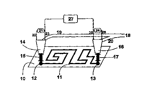
In Fig 1, numeral 10 indicates the printed circuit board, or other
interconnects network, to which an embodiment of th~.: i :a.~c:ntion is
applied.
Numeral 11 indicates a circuit from pad 12 to pad 13, which is to be tested
by means of the invention. A plasma injector-electrode 14, hereinafter to be
described, is placed opposite to pad 12 so as to direct the plasma jet
generated by it onto said pad, as shown by arrow 15. Likewise, plasma
injector-electrode 16 is placed opposite pad 13, so as to direct the jet
generated by it onto said pad, as shown by arrow 17. Evidently, the points
can be at any location on any conductor in the circuit, not necessarily pads.
They can also be parts of different nets, as is in the case of insulation
test.
CA 02329781 2000-10-25
WO 99/56137 '1~- PCT/IL99/00091
Numeral 18 indicates a source of gas that feeds the two plasma injector-
electrodes 14 and 16 through 19 and 20 respectively. An electric circuit 21 is
connected to the two electrodes of plasma injector-electrode 14, hereinafter
to be described, through two lines 22 and 23. An electric circuit 24 is
connected to the two electrodes of plasma injector-electrode 16 through two
lines 25 and 26. An electric circuit 27 is connected to one electrode in each
plasma injector-electrode. The two plasma electrodes should preferably be
identical, but it is not strictly necessary.
Fig. 2 shows, in schematic axial cross-section, two possible plasma injector-
electrodes according to embodiments of the invention, which could be either
plasma electrode 14 or plasma electrode 16 of Fig. 1. 10 is once again the
printed circuit board, which rests on a surface 30. The plasma injector-
electrode 14 is illustrated as being conical, though it is not necessary. Fig.
2a is an embodiment that comprises an outer layer 31 of insulating
material, a metal layer 32, which constitutes the second electrode and is
placed immediately inside the insulating layer 31, an intermediate
insulating layer 33, placed immediately inside the second electrode 32, and
another metal layer 34 which constitutes the first electrode and is placed
immediately within the insulating layer 33.
Electrode 34 defines a cavity 35, to which a gas is fed through a conduit
schematically indicated at 36. The gas stream fed into the plasma injector-
electrode flows therefore from top to bottom, as seen in the drawing, and
contacts firstly the first electrode 34, and then the second electrode 32, and
is transformed into plasma, by the voltage difference that is applied
between the two electrodes by the discharge circuit 37. The discharge gap is
defined by insulating layer 33, as indicated at 38. The plasma flows out of
nozzle 39 and forms a jet 40, which impinges on circuit board 10.
Fig. 2b is an embodiment that comprises a needle 4I, situated inside the
cavity in the insulation body 42. The needle is directed toward a metallic
CA 02329781 2000-10-25
WO 99/56137 -11- PCT/IL99/00091
nozzle 43, which acts also as the other electrode. The gap between the
needle and the nozzle, 44, is the discharge gap. The gas that flows through
this gap transforms into plasma by the discharge 45, and is injected through
the nozzle in a jet 46.
In the embodiments described so far, few separate plasma injector-
electrodes are provided and placed opposite the terminal pads of the circuit
to be tested. This requires displacing them when a different point of the
circuit is to be contacted. However, if the circuits to be tested, in an
interconnect network of any kind, or a plurality c~;~ch circuits, are
predetermined, the position of the terminal pads of ail said circuits are also
known, and then a plurality of plasma injector-electrodes can be provided
and placed in such positions that the circuit can be tested by selectively
activating the injector-electrodes that direct their plasma jets onto its
terminal pads. The injector-electrodes then need not be displaced to switch
from one point to another, and can be rendered solid or of one piece with one
another. In this case, the plurality of injector-electrodes may constitute an
injector-electrode system of simplified structure. Such a structure,
schematically, comprises four superimposed layers, two of them insulating
and two of them conducting, placed, from bottom to top, in the succession
insulating-conducting-insulating-conducting. The conducting layers
constitute the two electrodes, and the required voltages are applied by
circuit means as described in connection with the i~,e ~. iously described
embodiments. Registered openings are provided through the said layers, to
serve as plasma nozzles, opposite each terminal pad, and conduits are
provided to feed gas through said openings towards said terminal pad. The
gas, flowing through an opening, contacts firstly the first electrode (viz.
the
electrode more distant from the circuit to be tested), and then the second
electrode, and is transformed into plasma, which flows out of the nozzle and
forms a jet which impinges on the terminal pad opposite to it. Such a
structure may be considered, for example, as a plurality of injector-
electrodes similar to that of Fig. 2a, flattened out and rendered solid with
CA 02329781 2000-10-25
WO 99/56137 -12-
PCT/IL99/00091
one another. Another approach can be also used, where all said openings
are placed on a dense matrix, dense enough so that the spacing between two
adjacent openings will be the same as the closest pads to be tested. An
electric addressing mechanism is used to activate two injector-electrodes at
the time to perform a required test between the two pads above which they
are located.
Fig. 3 is an example of an electric circuit that may L~ used to carry out the
invention. The segments that are denoted by numeral 50 and 51 are the
discharge ignition and sustaining circuits, each of them is connected to the
two electrodes in one plasma injector-electrode. Preferably, they are
identical. The discharge circuits 50 and 51 comprise a high voltage pulse
source, V1 and V3 respectively, for the ignition, and a current source, I2 and
I4 respectively, for sustaining the discharge. The two circuits are connected
in parallel through the switches S1-4. Typical values that are required are
100-1000 volts for the ignition. Immediately after the ignition phase, the
discharge voltage falls to several tens volts, and a current level of 0.1-10
Amperes is required to in order to sustain it.
The segment that is denoted by numeral 52 is the m~asurei~ent circuit. It is
connected between one electrode of each of the plasma injector-electrodes,
but can be connected through an independent electrode. The circuit is closed
through the plasma contacts and the net being tested. This circuit
comprises a source V5, and voltage and current measuring means. In the
high resistance measurement mode (insulation test), the source acts as a
voltage source, and the low current level (several microamperes) is
measured accordingly. In the low resistance measurement mode (continuity
test), the source acts as a current source. In both cases, the net resistance
Rx is calculated by dividing the net voltage (after compensating for the
contact voltage) by the current through it. In the same manner, types of
impedance other than pure resistance can be measured.
CA 02329781 2000-10-25
WO 99/56137 -13- PCT/IL99/00091
Fig. 4 shows the probability in percent of failing to obtain a proper electric
contact with the pad through the plasma jet versus the distance between the
plasma injector-electrode and the pad. By 'proper' is meant a contact that
enables the measurement of the net resistance. This obviously depends on
the specific injector geometry and operating parameters; nevertheless, in
the specific case very good results were obtained up to a distance of 0.5 mm.
Fig. 5 shows the contact voltage versus the distance between the plasma
injector-electrode and the pad. Obviously, the voltage increases with the
distance, because the plasma has some resistance. Yet, ~.'':is dependence is
not too strong. This implies that there is some i~._: swat initial value of
contact voltage. This effect agrees well with the cathode and anode falls
that are described in the literature.
The Paschen curve that is presented in Fig. 6 gives the voltage that is
needed in order to ignite a discharge in various gases, versus the pxd value,
which is the discharge gap times the gas pressure. The most important
characteristic of this curve is its minimum, implying that the 'breakdown
voltage' is reduced when the electrodes are brought closer and the discharge
gap decreases, but below certain value this voltage increases again. In
argon in an atmospheric pressure, the minimum of Paschen is at a
discharge gap of about 50 microns. Preferably, the discharge gap in our
plasma injector electrode is designed to operate at the mi::ilnum of Paschen
curve.
Fig. 7 presents the I-V curve (load curve) for electric discharge. For our
application, a region with low voltage fall is required. For the high
resistance measurements we are using the leftmost region, while for the low
resistance measurements we are using the rightmost region (the arc region)
which is also the region in which our plasma source works.
CA 02329781 2000-10-25
WO 99/56137 ~ . .~ .... .. . PCT/IL89/OOQ91
~1 .~ ~ ~ ~ ~ D r v ~ ~
~ ~ ~ ~ ~~~ ~ ~ ~ f ~
~ ~ . r ~ 1 t ~~~~ 1 ~ ~ ~ ~
f 1 ~ ~ ~ ~ ~ ~ ~ ~ ~
~ i~~~ ~~~ ~~ ~ ~. ~~
- 14-
Although embodiments of the invention have been described by way of
illustration, it will be understood that the invention may be carried out
with many variations, modifications and adaptations, without exceeding
the scope of the claims.
~M~NDED SHEET