Note: Descriptions are shown in the official language in which they were submitted.
CA 02329924 2003-O1-14
DIFFUSING IMAGER AND ASSOCIATED METHODS
BACKGkOUND OF THE INVENTION
Field of the Invention
The present invention is directed to an optical element having a single
surface
which both diffuses light and has optical power.
Description of kelated Art
Diode lasers, LEDs and other light sources produce beams having a nonuniform
power distribution. This non-uniformity is often detrimental to performance of
a system.
It is difficult to achieve uniform power distribution using a conventional
lens system.
Elements which could be used to re-map the power distribution to one having
uniform
illumination are desirable for many applications.
It is advantageous to use a diffractive diffuser as shown in Figure l, to
provide the
desired uniform illumination. T'he diffractive diffuser in Figure i is
discussed in detail in
L1.S. Patent No. 5,850,300 ~;ntitled "Beam 1~Iomogenizer" issued December 15,
1998.
In Figure l, an incident optical beam 14, preferably a collimated beam,
illuminates a
- diffractive diffusing element 10.
CA 02329924 2000-10-24
WO 99/56182 PC'T/US99/08910
-2-
The diffractive diffusing element is preferably a computer-generated hologram
having
irregularly patterned, free-form fringes of diffractive gratings 12. The
diffractive fringes
12 of the preferred embodiment are made up of plateaus 16, shown as white
areas and
presenting a phase shift of zero at the design wavelength to the input beam
14, and vias
or valleys 1$, shown as black areas and presenting a phase shift of n at the
design
wavelength to the input beam. Such a homogenizes eliminates undesired
intensity
variations encountered when using a homogenizes having regularly shaped,
regularly
patterned facets.
The diffractive diffuser 10 transmits transmittal beams 11a, 11b, llc having a
preselected angular spread which provides a beam having uniform illumination
at a target
in an output plane 22. The output plane 22 represents an area in space rather
than any
particular element. It would be possible to place another optical element or
any device
which would make use of the output beam downstream. Any area of sufficient
size, i.e.,
to insure that the full range of line widths present in the pattern, at any
position on the
15 diffuser 10 will provide this angular spread to the input beam 14. Each
area of sufficient
size is nominally uncorrelated to another area of similar size. The choice of
angular
spread depends upon the application for which the homogenizes is used and the
desired
output beam.
Often, it is desirable to deflect or focus an image, as well as to diffuse it.
However,
20 due to space considerations for some applications, it is not convenient to
insert an
additional optical element for providing diffuse illumination. Further, there
is an
additional expense associated with making an additional element.
CA 02329924 2000-10-24
WO 99/56182 PCTNS99/08910
-3-
~UMM,ARY OF THE INVENTION
The present invention is therefore directed to an optical element, and
associated
systems and methods, which substantially overcomes one or more of the problems
due
to the limitations and disadvantages of the related art.
It is therefore an object of the present invention to provide a diffractive
diffusing
optical element in a single surface which can map non-uniform illumination
into more
uniform illumination and perform additional optical functions on the input
light. The
integration of both diffusing and other optical functioning on a single
surface provides
advantages such as space savings and does not increase the cost over making a
diffractive
performing only the other optical functions, since no additional surface needs
to be made.
The surface incorporating the diffusing function is created during the design
phase and
the resulting element costs the same to manufacture as an optical element
without the
diffusing function incorporated therein.
At least one of these and other objects may be realized by providing an
optical
element including a computer generated hologram for performing at least one
lens
function and at least one diffusing function, the computer generated hologram
including
free form regions having a phase shift associated therewith, the computer
generated
hologram being shifted within the free form regions by the phase shift
relative to the
computer generated hologram outside the free form regions, the computer
generated
hologram being on a first surface of the optical element.
The computer generated hologram outside the free form regions may include zero
regions and n regions, the zero regions and ~t regions being transposed within
the free
CA 02329924 2000-10-24
WO 99/56182 PCT/US99/08910
-4-
form regions. The at least one lens function may include at least one of
focusing and
deflecting. The optical element may further include features provided on a
second surface
of the optical element opposite the first surface and aligned with the
computer generated
holograms. The features may also perform the at least one lens function. The
features
may include a Fresnel lens. The phase shift may be n.
At least one of the above and other objects may be realized by providing a
method
of making a diffractive diffusing lens, including generating a computer
hologram pattern
in accordance with a desired lens function and a diffusing function, the
computer
hologram including a plurality of free form regions having a phase shift
associated
therewith, within the free form regions, the computer hologram is shifted by
the phase
shift relative to the computer hologram outside the free form regions, and
manufacturing
the diffractive diffusing lens in accordance with the computer hologram
pattern.
The manufacturing may include photolithographic processing. The manufacturing
includes injection molding. The generating may include transposing the
computer
hologram within the free form regions.
At least one of the above and other obj ects may be realized by providing an
optical
system including a light source, transmit optics for delivering light from the
light source
to a target, and return optics for receiving light from the target, wherein at
least one of the
transmit optics and the return optics includes a diffractive diffusing lens
providing
diffusion and at least one lens function on a single surface.
The transmit optics and return optics may be integrated on a single substrate.
The
diffractive diffusing lens may include a computer generated hologram for
performing at
CA 02329924 2000-10-24
WO 99/56182 PCTNS99/08910
-5-
least one lens function and at least one diffusing function, the computer
generated
hologram including free form regions having a phase shift associated
therewith, the
computer generated hologram being shifted within the free form regions by the
phase shift
relative to the computer generated hologram outside the free form regions, the
computer
generated hologram being formed on the single surface. The transmit optics may
include
the diffractive diffusing lens.
Further scope of applicability of the present invention will become apparent
from
the detailed description given hereinafter. However, it should be understood
that the
detailed description and specific examples, while indicating preferred
embodiments of the
invention, are given by way of illustration only, since various changes and
modifications
within the spirit and scope of the invention will become apparent to those
skilled in the
art from this detailed description.
BRIEF DESCRIPTION OF THE DRAWINGS
The present invention will become more fully understood from the detailed
description given hereinbelow and the accompanying drawings which are given by
way
of illustration only, and thus are not limited to the present invention and
wherein:
Figure 1 illustrates the spatial energy distribution of a beam incident upon a
homogenizes including free form, irregularly patterned plateaus and vias and
the resultant
uniform power distribution;
Figure 2 is a side view of a configuration incorporating a diffractive
diffusing
optical element of the present invention;
CA 02329924 2000-10-24
WO 99/56182 PCT/US99/08910
-6-
Figure 3A is a top view of an optical apparatus including the diffractive
diffusing lens of the present invention;
Figure 3B is a side view of the optical apparatus in Figure 3A;
Figure 4A illustrates fringes of part of a mask for the imager alone;
Figure 4B illustrates fringes of part of a mask for the diffuser alone;
Figure 4C illustrates fringes of part of a mask for constructing the
diffractive
diffusing imager of the present invention; and
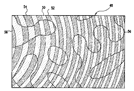
Figure 5 illustrates fringes of part of the diffractive diffusing imager of
the
present invention.
DETAILED DESCRIPTION OF PREFERRED EMBODIMENTS
While the present invention is described herein with reference to illustrative
embodiments for particular applications, it should be understood that the
present
invention is not limited thereto. Those having ordinary skill in the art and
access to the
teachings provided herein will recognize additional modifications,
applications, and
embodiments within the scope thereof and additional fields in which the
invention would
be of significant utility without undue experimentation. As used herein, the
term "lens
function" means a function having optical power.
Figure 2 illustrates a configuration incorporating the optics of the present
invention. A light source 28, preferably a light emitting diode, emits light
toward a
transmit optical apparatus 30. The transmit optical apparatus 30 delivers
light to a target
34. Light reflected by the target 34 is delivered to a detector 38 via a
return optical
CA 02329924 2000-10-24
WO 99/56182 PCT/US99/08910
_7_
apparatus 36.
Preferably, the optical apparatuses 30, 36 are integrated on a common
substrate 40,
and the light source 28 and the detector 38 are integrated on a common
substrate 42. As
can be seen in the configuration of Figure 2, the transmit optical apparatus
30 focuses the
light from the light source 28 onto the target 34.
Further details of the optics are shown in Figures 3A and 3B. The top view in
Figure 3A illustrates the integration of the optical apparatuses 30, 36 onto a
single
substrate 40. As shown in the side view of Figure 3B, the return optical
apparatus 36
includes a diffractive element 44 on a fzrst surface and a refractive element
45 on a second
surface.
As can also be seen in the side view of Figure 3B, the transmit optical
apparatus
30 includes a diffractive element 46 on a first surface thereof and a Fresnel
element 47
on a second surface thereof. Both of these elements 46, 47 are needed in the
transmit path
due to the large deflection angle required in the configuration shown in
Figure 2. Without
the use of the diffractive element 46, total internal reflection greatly
limits the amount of
power that can be directed onto a target. If only the diffractive element 46
is used, the
large deflection angle required will result in greatly reduced diffraction
efficiency.
A diffusing element is also incorporated into the diffractive element 4b on
the first
surface. Thus, the diffractive element 46 serves three functions. It will
provide
approximately half of the required deflection angle. It will aid in focusing
light onto the
target. It will diffuse and homogenize the light to a more uniform intensity
distribution
in the illumination region of the target.
CA 02329924 2003-O1-14
A binary mask 48a for making a diffractive for performing a lens function is
shown in Figure 4A. Hatched regions 52 present a phase shift of zero and white
regions
'~4 present a phase shift of n to the design wavelength. These regions or
fringes
respectively correspond to plateaus and vias on the surface itself. In the
design shown in
F' figure 4A, adjacent hatched or 0 regions and white or ~ regions have the
approximately
the same width. If only two levels are desired in the diffractive diffusing
lens, then the
lens will look like this mask 48.
The annular fringes required to create a diffractive for performing the lens
functions may
be computer generated in a conventional manner.
A binary mask 48b for making a diffractive diffuser is shown Figure 4B. An
example of a diffractive diffuser that would be made from such a mask is shown
in Figure
1. The hatched regions 53 present a phase shift of n and the white regions 55
present a
phase shift of zero to the design wavelength. These regions or fringes
respectively
c;oirespond to vias and plateaus on the surface itself. If only two levels are
desired in the
diffractive diffuser, then the lens will look like this mask 48b. Such a
diffuser may be
designed as set forth in U.S. Patent l~.~o. 5,850,300. Generally, these
regions may be described
as free from regions. The use of free fiom rc;gions to provide the diffusing
function
eliminates undesired intensity variations due to sharp edges between the TI
and 0 regions.
A binary mask 48c for making a diffractive element 46 incorporating lens
functions, such as deflection and focusing, as well as the diffusing function
is shown in
Figure 4C. In accordance with the present invention, the diffusing imager may
be created
CA 02329924 2003-O1-14
..g_
by adding the phases of the two functions forming the masks shown in Figures
4A and
4B. Such an addition results in shifting the base lens function pattern 54
within the n
regions 53, creating shifted regions 56, to form a diffractive diffusing lens
on a single
surface. In the zero regions 55 of the diffusing mask 48b, the lens function
pattern 54 is
unaffected. In the specific example of a portion of a mask 48c shown in Figure
4c, the 0
regions 52 and the n regions 50 within the diffuser n regions 53 are shifted
in the
resultant shifted regions 56 sufficiently so that they appear transposed from
those in the
lens function region 54.
The shifting resulting from the incorporation of the diffusing function will
result
in a slight loss of power from the base lens function, i.e., the point will be
slightly blurred.
The blur is due to the fact that while a lens maps to a point, the diffuser
maps to a region,
as described above in connection with Figure 1. The amount of blur will depend
on the
design of the diffuser. In order to achieve the diffusing function preferably
between
approximately 5% and 50% of the surface is encompassed by the shifted regions.
1 S The mask 4$c may be used in accordance with United States Patent No.
4,895,790.
the entirety of which is hereby incorporated by reference, to create optical
elements
haviftg plateaus and vias using binary masks. Further, United States Patent
No. 5,202,775,
which is hereby incorporated by reference in its entirety, discloses a method
of fabricating
holograms using photolithography and LJ.S. Patent No. 5,728,324, issued on
March 17, 1998,
discloses a method of fabricating diffi-active elements using injection
molding. The mask
tray thus be used with a variety of methods to form the diffractive diffusing
lens in
accordance with the present invention.
CA 02329924 2000-10-24
WO 99/56182 PCT/US99/08910
-10-
An actual diffractive diffusing lens in accordance with the present invention
is
shown in Figure S. The element S8 shown in Figure S can be made using two or
three
masks, depending on the technique used, and has four levels or regions, the
white or n
region S0, presenting a phase shift of 7z, the large dot region S7 presenting
a phase shift
of ~/2, the black or 0 regions S2, and the small dot region S9 presenting a
phase shift of
3n/2. All ofthe notedphase shifts are at the design wavelength. The n/2 and
3~c/2 regions
will actually appear as gray regions, but the dots were used to facilitate
visibility. As with
the mask 48c, the element S8 has lens function or original regions S4 and
shifted regions
Sb, in which the base lens function pattern is shifted to provide the
diffusing function. In
the example shown in Figure S, the shifting in the free form regions S6 is two
levels from
the original regions S4.
Each mask used to create the element S 8 does not have to have the diffizsing
function incorporated therein. The element S8 shown in Figure S only had one
mask with
the diffusing function incorporated with the base lens function, i.e., mask
48c shown in
1 S Figure 4. The other masks were for forming only the base lens function.
Preferably, if
only one mask has the diffusing function incorporated, it is the mask for the
primary or
biggest etch.
The invention being thus described, it will be obvious that the same may be
varied
in many ways. Such variations are not to be regarded as a departure from the
spirit and
scope of the invention, and all such modifications as would be obvious to one
skilled in
the art are intended to be included within the scope of the following claims.