Note: Descriptions are shown in the official language in which they were submitted.
CA 02330537 2000-10-27
WO 99/57789 PCTNS99/09607
VERTICAL-CAVITY SURFACE-EMITTING LASER WITH AN
INTRACAVITY QUANTUM-WELL OPTICAL ABSORBER
This application is a continuation-in-part of the application entitled
"Intracavity
Quantum Well Photodetector l:ntegrated within a Vertical-Cavity Surface-
Emitting
Laser", Serial Number 08/731 "527, filed October 16, 1996, now issued as U.S.
Patent
This invention was made with Government support under Grant (Contract) No.
N00014-96-1-0583, awarded by the Office of Naval Research. The Government has
certain rights to this invention,
Brief Description of the Invention
This invention relates generally to lasers. More particularly, this invention
relates to a vertical-cavity surface-emitting laser with a wavelength-
dependent
intracavity optical absorber, which may be used as an integrated detector, a
self
pulsating laser, a high speed intracavity modulator, or an optical pick-up
device.
Background of the Invention
Vertical-cavity surface:-emitting lasers (VCSELs) are used as light sources in
a
variety of electronic applications including fiber optic communications, laser
printing,
and optical data storage. A VCSEL is an injection diode laser where the laser
oscillation and output occur normal to a semiconductor pn junction plane. In
edge-
emitting laser diodes, the laser oscillation and output occur in the
semiconductor pn
junction plane. VCSELs havE: many advantages compared with edge-emitting laser
CA 02330537 2000-10-27
WO 99/57789 PCTNS99/09607
diodes. These advantages include a low divergence circular output, single
longitudinal
mode operation, and high two-dimensional packing density.
All lasers use the princiiple of amplification of electromagnetic waves by
stimulated emission of radiation. The term Iaser is an acronym for light
amplification
by stimulated emission of radiation.
The process of stimulated emission can be described as follows. When atoms,
ions, or molecules absorb ener,~gy, they can emit light spontaneously (as in
an
incandescent lamp) or they cara be stimulated to emit by a light wave. If a
collection of
atoms is pumped so that more are initially excited than unexcited, then an
incident
light wave will stimulate more emission than absorption, and there is net
amplification
of the incident light beam. This is the way a laser amplifier works.
A laser amplifier can b~e made into a laser oscillator by arranging suitable
minors on either end of the arr~plifier to form a resonator. Thus, the
essential parts of
a laser oscillator are an amplifying medium, a source of pump power. and a
resonator.
Radiation that is directed straiF;ht along the axis bounces back and forth
between the
mirrors and can remain in the resonator long enough to build up a strong
oscillation.
Radiation may be coupled by making one minor partially transparent so that
part of
the amplified light can emerge through it.
The fundamental light-producing mechanism in an injection diode laser. such
as a VCSEL, is the recombina~cion of excess conduction-band electrons and
valence-
band holes. This recombination operation takes place by pumping excess
carriers
across a junction. That is, excess electrons are injected from a semiconductor
n-layer
and excess holes from a semiconductor p-layer into an active waveguide region,
where
they recombine, via stimulated emission, producing the desired gain. The
losing
threshold is reached when optical loss is balanced by optical gain.
Many applications of semiconductor lasers require dynamic stabilization of the
light output against variations in the external environment. It is also
necessary to
monitor long-term drift in the laser and its drive circuitry. In most
commercially
available diode lasers, this is clone by using a discrete external monitoring
photodiode
chip. The photocurrent generated by the external detector is used in a
feedback circuit
to adjust the Iaser injection current.
2
CA 02330537 2000-10-27
WO 99/57789 PC'f/US99/09607
Recently, it has been proposed to substitute discrete external monitoring
photodiode chips with monolithic photodiodes for the use with VCSELs. In these
schemes, photodiodes are placed either on the top, on the bottom, on the side,
or along
the perimeter of the VCSEL. In this location, the photodiode directly
intercepts and
samples the laser emission as it exits the device.
While the monolithic approach avoids many of the problems associated with
the use of a separate monitorin~; photodiode chip, its performance is far from
ideal.
The primary problem with these devices is that they detect too much
spontaneous
emission. In addition, they are susceptible to ambient light. Consequently,
the
performance of the proposed monolithic photodiodes is inferior to that of a
separate
monitoring photodiode chip. Thus, it would be highly desirable to develop an
improved monolithic photodetector for use in VCSELs.
In addition to the need for improved monolithic photodetectors for use in
VCSELs, there is a need for improved modulation of VCSELs at high frequencies.
Primary characteristics of interest in VCSEL modulation include high speed,
high
modulation depth, and low frequency chirp. Depending on the modulation
technique
and the application involved, my combination of these features may be
manifested.
For example, an external modulator integrated with a VCSEL eliminates
frequency
chirping since the modulating element is outside the lasing cavity. However,
if the
absorption layer is thin (i.e., a single quantum well), then the speed is high
but the
small single-pass absorption leads to low modulation depth. If the absorption
layer is
thick, the thickness required for a bulk layer would be very large, requiring
large
voltages to achieve the same electric field as that across a single quantum
well since
the interaction length in a vertical cavity is much shorter than that in an in-
plane laser.
Multiple quantum wells would number in the tens or hundreds - an impractical
growth.
Direct current modulation has been demonstrated for high speeds and high
modulation depths. However, the changes in carrier density introduce frequency
chirp,
which may not be suitable for applications where frequency stability is
required.
One technique to obtain modulated light output from a VCSEL is to generate
self pulsation in the device. A self pulsating VCSEL has an AC output derived
from a
DC input. Known self pulsating lasers are edge-emitters. It would be highly
desirable
to develop a self pulsating VCSEL because the surface-normal geometry would
3
CA 02330537 2000-10-27
WO 99157789 PCT/US99J09607
facilitate two-dimensional array configurations and wafer-scale fabrication.
In
addition, the circular beam ouput of the VCSEL could be exploited.
Although self pulsation in VCSELs has been previously analyzed and observed
with repetition rates up to the MHz range, no VCSEL has yet been observed to
self
pulsate at high frequency or with a controllable saturable absorber. In the
prior art, the
self sustained oscillations have been observed by introducing, intentionally
or
inadvertently, saturable absorbing centers surrounding the device cavity. In
view of
the foregoing, it would be highly desirable to provide a VCSEL with improved
self
pulsation through a wavelength dependent intracavity quantum-well absorber.
Lasers are used in the prior art for optical pick-up detection. However.
current
optical disk readout schemes use an edge-emitting laser as the optical source
and a
separate external photodetector. It would be highly desirable to integrate the
optical
source and detector into a singlle device. Such an approach would eliminate
noise due
to reflections from unncessary bulk optics and also minimize the physical size
of the
device. It would also be desiraible to use an end-emitting laser, the circular
beam
output of which would allow the the output beam to be focussed tp a spot size
that is
smaller than that of an edge-emitting device. Focusing the beam to a smaller
spot size
would increase the allowable information density on the optical disk.
In sum, it would be highly desirable to develop an improved VCSEL to
overcome the foregoing limitations associated with prior art VCSEL technology.
Summary of the Invention
A laser comprises a first contact to receive an active region control signal.
a
second contact to receive an optical absorber control signal, and a sandwich
of
distributed Bragg reflector mirror stacks. Each distributed Bragg reflector
mirror stack
has an alternate doping with reapect to an adjacent distributed Bragg
reflector minor
stack. An active region is positioned in the sandwich to provide optical gain
in
response to the active region control signal. An optical absorber is
positioned in the
sandwich. The optical absorber has wavelength dependent absorption.
The laser or VCSEL structure itself has a characteristic transmission
wavelength that is deliberately designed. In conjunction with the biasing
circuitry
used to apply a signal to the absorber, the designable position of this
characteristic
4
CA 02330537 2000-10-27
WO 99/5'I789 PCT/US99/09607
transmission wavelength (also called Fabry-Perot wavelength) relative to the
absorber
band-edge determines the function of the device. The Fabry-Perot wavelength
and the
absorption band edge results in different device functions. The Fabry-Perot
wavelength and the absorption band edge can be designed so that the absorber
is
characterized by a negative differential resistance when its current-voltage
trace is
measured. Depending on how the absorber is biased (i.e., what sort of load
line/external circuitry is applied to the absorber), the device can exhibit
(a) bistability
and hence be used for optical pick-up detection or (b) self pulsations. In the
optical
pick-up configuration, the primary function of the absorber is to (a) detect
the signal
from external feedback and (b) amplify the response signal through the
bistability that
results from the carefully designed absorber and VCSEL structure. The optical
pick-
up configuration provides a low noise, compact alternative to existing bulk
edge-
emitter and external photodetector readout schemes.
The device of the invention also has a number of benefits over edge-emitting
devices of the prior art. These benefits include circular beam output, wafer
scale
fabrication, and potential two-dimensional array configurations.
Brief Description of the Drawings
For a better understandling of the nature and objects of the invention,
reference
should be made to the following detailed description taken in conjunction with
the
accompanying drawings, in wlhich:
FIGURE 1 is a cross-sectional view of an injection diode laser constructed in
accordance with an embodiment of the invention.
FIGURE 2 illustrates the intensity-field distribution within the resonating
cavity of a bottom-emitting device in accordance with an embodiment of the
invention.
FIGURE 3 illustrates the intensity-field distribution within the resonating
cavity of a top-emitting device in accordance with an embodiment of the
invention.
FIGURE 4 illustrates light-current (L-1) characteristics of bottom-emitting
devices as detected by the intracavity (or internal) and external
photodetectors in
accordance with the invention.
5
CA 02330537 2000-10-27
WO 99/57789 PCT/US99/09607
FIGURE 5 illustrates light-current (L-I) characteristics of top-emitting
devices
as detected by the intracavity (or internal) and external photodetectors in
accordance
with the invention.
FIGURE 6 illustrates light-current (L-I) mismatch due to lasing wavelength
red-shifting through the detector quantum well excitonic peak.
FIGURE 7 illustrates minimal detected spontaneous emission for a top-
emitting device constructed in accordance with an embodiment of the invention.
FIGURE 8 illustrates minimal detected spontaneous emission for a bottom-
emitting device constructed in accordance with an embodiment of the invention.
FIGURE 9 illustrates that a device in accordance with the invention is much
less sensitive to external light than an external photodetector.
FIGURE 10 illustrates; the dark current associated with a device constructed
in
accordance with an embodiment of the invention.
FIGURE 11 illustrates. the effective detectivity of the internal detector as a
function of laser pump current for a device constructed in accordance with the
invention.
FIGURE 12 illustrates the effective detectivity of three devices constructed
in
accordance with the invention, showing increased detectivity with increasing
wavelengths.
FIGURE 13 illustrates the voltage behavior of a device in accordance with an
embodiment of the invention.
FIGURE I4 illustrates the output spectra of a top-emitting device in
accordance with an embodiment of the invention.
FIGURE 15 illustrates an air bridge contact structure in accordance with an
embodiment of the invention.
FIGURE 16 illustrates a ridge waveguide structure in accordance with an
embodiment of the invention.
FIGURE 17 illustrates buried heterostructure layers in accordance with an
embodiment of the invention,
FIGURE i 8 illustrates a proton implantation current confinement structure in
accordance with an embodiment of the invention.
6
CA 02330537 2000-10-27
WO 99/57789 PCTNS99/09607
FIGURE 19 illustrates a VCSEL with an intracavity quantum-well absorber in
accordance with an embodiment of the invention.
FIGURE 20 illustrates a bias-T circuit operated in connection with an
embodiment of the invention.
FIGURE 21 illustrates a circuit that may be used to accumulate measurements
associated with the operation of a device constructed in accordance with the
invention.
FIGURE 22 illustrates the L-I,u« and I,,Se~ V,aS« characteristics of a device
constructed in accordance with an embodiment of the invention.
FIGURE 23 illustrates .device response to absorber modulation under several
DC bias conditions (I,~~).
FIGURE 24 illustrates 'bandwidth as a function of laser bias current for a
device constructed in accordance with an embodiment of the invention.
FIGURE 25 illustrates .a relatively constant bandwidth associated with
absorber
modulation response for fixed laser bias currents at different DC absorber
biases.
FIGURE 26 illustrates output power as a function of bias current for a device
of the invention.
FIGURE 27 illustrates absorber Ia-Va characteristics for a device of the
invention.
FIGURE 2$ illustrates the measured absorption as a function of wavelength for
different reverse bias voltages. The lasing wavelength is shown as a vertical
line in the
figure to illustrate the variation in the relative absorption seen by the
laser as the
absorption spectrum shifts with reverse bias voltage.
FIGURES 29(a)-29(d) illustrate self pulsation characteristics of a device of
the
invention.
FIGURE 30 shows a plot of self pulsating frequency as a function of laser bias
current Ig.
FIGURES 31 (a)-31 (b) illustrate the device of the invention configured as an
optical pick-up device.
FIGURE 32 shows the desired L-Is trace for the device of Figure 31 under
typical bias conditions.
FIGURE 33 illustrates that the optical switching of the device of Figure 31 is
accompanied by a switching of the voltage Va across the integrated absorber.
7
CA 02330537 2000-10-27
WO 99157789 PCTNS99/09607
FIGURE 34 illustrates absorber I,-Va traces with and without feedback and the
load line corresponding to sele;cted bias conditions.
FIGURE 35 illustrates the device of the invention operated as an optical disk
readout device.
FIGURES 36(a)-36(b) illustrate the absorber current versus voltage (Ia Va)
traces measured for the device of the invention under different design
criteria; in
Figure 36(a) the device is designed with the Fabry-Perot wavelength shorter
than the
absorber band-edge; in Figure 36(b) the device is designed with the Fabry-
Perot
wavelength longer than the absorber band-edge, resulting in an h-Va response
exhibiting negative differential resistance.
FIGURE 37 illustrates the selection of the DC absorber bias (R and Va in
Figure 20 and R,+R, and Vo in Figure 31 ) such that the operating load line
intersects
the absorber current versus voltage (Ia-Va) trace three times. This choice of
load line
yields bistable device operation.
FIGURE 38 illustrates the selection of the DC absorber bias (R and Vo in
Figure 20) such that the operating load line is tangential to the absorber
current versus
voltage (Ia Va) trace. This choice of load line yields self pulsation of the
device.
Like reference numerals refer to corresponding parts throughout the several
views of the drawings.
Detailed Description of the Invention
Figure 1 illustrates an intracavity quantum well photodetector integrated
within
a vertical-cavity surface emitting laser 20 in accordance with an embodiment
of the
invention. In one embodiment of the invention, the apparatus 20 includes an n+
doped
GaAs substrate 22. Grown on the substrate 22 is an n-doped distributed Bragg
reflector (DBR) minor stack ;?4. DBR minor stacks are known in the art. In
particular, the optimization of such a structure for a particular application
is known in
the art. An active gain region. 26 is constructed on top of the n-doped DBR
mirror
stack 24. The active gain region 26 includes a one-wavelength spacer 28 with a
quantum well stack 30 positioned therein. The quantum well stack 30 includes
two
80-Angstrom thick Ino.,Gao,gAs quantum wells.
8
CA 02330537 2000-10-27
WO 99/57789 PCT/US99/09607
A p-doped DBR minor stack 36 is positioned on top of the active gain region
26. One or more current confinement layers 38 are formed within the stack 36.
The
current confinement layer 38 is~ 3 DBR pairs away from the active region 26.
The
current confinement layer 38 may be in the form of a 3/4~,-thick AIAs
(aluminum
arsenide) oxidation layer. An oxidation layer of AlxGa,_~As, where x is
approximately
one, may also be used. In the aternative, an air gap may be used. The air gap
may be
formed by etching a sacrificial layer. Thereafter. regrowth may be executed or
an air
bridge may be constructed. Proton implantation by shadow masking or a similar
technique may also be used to form a current confinement layer. An annular
contact
40 is formed on the p-doped DBR mirror stack 36.
An intracavity quantunn well photodetector 50 is then formed on the p-doped
DBR minor stack 36. The intracavity quantum well photodetector SO includes a
5~,/4
spacer 52 with one 80-A Ina.~Gao BAs (indium gallium arsenide) quantum well 54
formed therein as the detector.
I S An n-doped DBR mirror stack 60 is then grown on top of the intracavity
quantum well photodetector SCI. An n-contact 62 is deposited on top of the
device 20.
The p-contact 40 is deposited after etching down to the p+ doped layers of the
p-doped
DBR minor stack 36. The p-contact 40 is used to forward bias the active region
32,
while the n-contact 62 is used to control the voltage across the quantum-well
detector
50. Further, contacts 62 and 4~0 are used to bias the detector. The laser is
biased using
contact 40 and the substrate 2f..
In the embodiment of Figure 1, light comes out of the bottom surface 70 of the
substrate 22. Thus, it is referrE;d to as a bottom-emitting device. The device
can also
be designed to have light come; out of the top surface. A top-emitting device
may be
constructed with an annular N~-contact which allows light to escape through
its
aperture. A different configuration of DBR pairs is used in a top-emitting
device. In
sum, Figure 1 illustrates an err~bodiment of the invention wherein an n-p-n
VCSEL
device 20 is defined. In general. the device operates in a manner that is
consistent with
existing VCSEL devices. That is, excess charge carriers are injected from the
n-layer
and p-layer regions of the device into the active region 26. The fasing
threshold is
reached when the optical loss ;is balanced by the optical gain. In prior art
devices, this
operation is monitored by a discrete external photodetector or a photodetector
9
CA 02330537 2000-10-27
WO 99/57789 PCT/US99/09607
constructed on the top or bottom of the VCSEL. However, in accordance with the
invention, the device is operated in conjunction with the intracavity quantum
well
photodetector S0. That is, the intracavity quantum well photodetector 50 of
the
invention provides an improved photocurrent for use in a standard feedback
circuit
which is used to adjust the laser injection current in a standard manner.
Naturally, the
improved photocurrent signal can be used for other purposes as well.
Particular
benefits of this intracavity quantum well photodetector 50 are discussed
below.
Attention presently turns to a discussion of processing steps that may be used
to
construct the device of the invention.
The apparatus of Figurf: 1 may be constructed in any number of ways. One
advantage of the invention is that its processing steps are consistent and
compatible
with well known processing stt:ps. The following processing steps may be used
in
accordance with one embodiment of the invention.
A wafer is grown on a ~3aAs substrate via molecular beam epitaxy with a
refractive index profile as shown in Figure 2. Waveform 82 of Figure 2
illustrates the
intensity-field distribution within the resonant cavity defined by the DBR
stacks 24
and 36. The peaks of the intensity-field distribution overlap with the quantum
wells.
The discontinuity of waveforrr~ 80 shown within the circled region 84
corresponds to
the spacer of the quantum well detector 50. The peak 86 corresponds to the
quantum
well 54.
The wafer is then diced into smaller units for ease of processing. A layer of
AIAs is then oxidized to provide a current confinement layer. This is done by
patterning the sample by standard photolithography to produce 90-micron
circles of
photoresist. The sample is then etched with a 1:8:40 sulfuric acid:hydrogen
peroxide:deionized water soluvtion until the AIAs layer is exposed. The
photoresist is
then washed off; using acetone: followed by methanol. The sample is then
placed in an
oxidation furnace (flowing water vapor at approximately 425 degrees Celsius)
until the
desired aperture is achieved. 'the oxidation time usually needs to be
calibrated first.
The desired aperture is around. 10 microns in diameter.
Next, the n-contact 62 is deposited. This may be done by patterning the
sample using standard photolithography to produce approximately 20-micron
circles
of photoresist centered over the 90-micron etched circles. Evaporation of 150
CA 02330537 2000-10-27
WO 99/57789 PCT/US99/09607
Angstroms of nickel, 350 Angstroms of germanium, 500 Angstroms of gold, 350
Angstroms of nickel, and finally 1500 Angstroms of gold is then performed. The
photoresist is then stripped, using acetone followed by methanol.
The p-contact 40 is then formed. This may be done by patterning the sample
using standard photolithography to produce approximately 34-micron diameter
circles
of centered photoresist. The sample is then etched in 1:8:40 sulfuric
acid:hydrogen
peroxide:deionized water until the p+ doped layers are reached. The sample is
then
dipped in 10:1 buffered oxide Each or I :40 hydrofluoric acid:deionized water
to clean
off any AIGaAs oxides. The photoresist is then washed off. The sample is then
patterned by standard photolithography to produce annular dark-field rings
(centered)
about 70 microns in diameter and 16 microns in annulus width. Approximately
200
Angstroms of titanium and 2000 Angstroms of gold are then evaporated. Finally,
the
photoresist is washed off.
Similar steps are performed for a top-emitting VCSEL with an intracavity
quantum-well photodetector. The n-contact is evaporated first followed by the
p-
contact. Then, the two metal contacts are annealed in a rapid thermal annealer
to
improve the conductivity. Finally, the sample is etched down and oxidized. The
intensity-field distribution within the cavity of a top-emitting device is
shown in
Figure 3.
The operation of the invention and its advantages are more fully appreciated
with reference to the followin~; figures. Figure 4 illustrates the Light-
Current (L-I)
characteristics of a bottom-emitting device in accordance with the invention.
This
figure compares the internal pllotodetector current and the external
photodetector
current (calibrated to milliwatts of output power). The two L-I curves match
very
closely. Virtually no spontaneous emission (incoherent random fluctuations of
light
that is emitted, most evident below the lasing threshold) is detected.
However,
because it is a bottom-emitting; laser, the backside reflections off the
substrate interface
causes ripples in the output power, as evident in the external detector trace.
The
ripples can be eliminated with the use of an anti-reflection coating. V~, is
the reverse
bias voltage applied to the internal photodetector.
Figure 5 illustrates the Light-Cunrent (L-1) Characteristics of top-emitting
devices. This graph compares the internal photodetector current and the
external
11
CA 02330537 2000-10-27
WO 99/57789 PC'f/US99/09607
photodetector current. The effective detectivity (or responsivity) is 1.2A/W.
Again.
virtually no spontaneous emission is detected by the internal detector. The L-
I curves
do not match as closely as in t;he case of the bottom-emitting device.
Figure 6 illustrates the critical nature of the relative alignment of the
Fabry-
S Perot wavelength (~,Fp) and the: absorber band edge (~.abf). In this case.
~,~p is longer
~~ f abs~ since these two wavelengths red-shift at different rates as
indicated, the
lasing wavelength (~.Fp) rides up the absorption curve with increasing pump
current
(increasing temperature) and hence experiences absorption that is not
constant. thereby
impacting the device as an accurate integrated detector.
Figure 7 illustrates minimal detected spontaneous emission for a top-emitting
device, while Figure 8 illustrates minimal detected spontaneous emission for a
bottom-
emitting device. These figures actually magnify the behavior of the L-I curves
from
previous figures so that one can more clearly observe the spontaneous
emission. For
both bottom- and top-emitting, structures, the amount of spontaneous emission
detected
by the internal detector is as low as (in the bottom-emitting case) and even
lower (in
the top-emitting case) than an external detector. This effect is due to the
fact that the
quantum well is placed at a resonant position to detect only the Fabry-Perot
wavelength and hence is not as sensitive as bulk material to the broadband
nature of
spontaneous emission.
Figure 9 illustrates the response of a top-emitting device to external light.
In
particular, the figure shows how insensitive the device is to external light.
The solid
lines represent the internal and external detectors without any external light
applied to
an experimental measurement setup. The dotted lines show the responses when
external light is shone onto the setup. The external detector response shows a
large
jump. while the internal detector is virtually unaffected.
Figure 10 illustrates the dark current characteristics of the.device of the
invention. The dark current is the amount of current that the detector
exhibits when
there is no light or signal for it to detect. The lower the dark current, the
more
sensitive the detector is to any signal. The device of the invention
demonstrates pA
(picoAmperes) of dark current, which is as low as any commercially available
detector. In fact, the measurements have been limited by the measuring
instrument's
noise floor so that the true da~~k current may be even lower.
12
CA 02330537 2000-10-27
WO 99/57789 PCTNS99/09607
Figure 1 I illustrates the: internal effective detectivity of a device of the
invention. The figure shows the effective detectivity as a function of the
laser ptunp
current. The effective detectivity is at least lA/W around the threshold. This
high
responsivity results from tailoring the detector quantum well's overlap with a
peak of
the intensity field distribution within the losing cavity. The detectivity's
increase with
pump current is a result of the losing wavelength shifting through the
detector' s
excitonic peak.
Figure 12 is a plot of the internal effective detectivity versus wavelength.
This
figure compares three devices of the same size and characteristics. The
effective
detectivity rises with increasingly longer wavelengths, bearing out the
explanation of
the excitonic enhancement due: to the detector quantum well.
Figure 13 illustrates Current-Voltage (I-V) Characteristics of a device of the
invention. The figure shows a device threshold voltage of 2.2V.
Figure 14 illustrates the spectra of a top-emitting device in accordance with
the
invention. The output spectra of a device is tailored for specific
applications. The
device of this example was designed to lose at 980 run. The actual wavelength
produced is around 966 nm, as shown in the plot. The device starts out single-
mode
(no side lobes due to transverse modes) and becomes multi-mode at longer
wavelengths with increasing pump current.
The invention has now been fully described. Attention presently turns to a
discussion of the benefits associated with the invention, followed by a
discussion of
alternate embodiments in accordance with the invention.
A primary benefit of the invention is that it avoids bulky external detectors
and
accompanying optics. Another primary benefit of the invention is that its
performance
is superior to that of other monolithic sensors that are positioned on the
top, bottom, or
side of a VCSEL. Advantageously, the embedded nature of the quantum-well
photodetector 50 between the p-doped DBR minor stack 36 and the n-doped DBR
mirror stack 60 renders the ph,otodetector highly insensitive to spontaneous
emission
and ambient light. This is in contrast to existing prior monolithic devices
where the
photodetector is essentially an external detector. The quantum well, with its
embedded
position, prevents stray light from interfering with the power detection and
monitoring,
while its thin active region miinimizes dark current.
13
CA 02330537 2000-10-27
WO 99/57789 PCT/US99109607
Advantageously, the device uses a quantum well as the detecting or absorbing
medium, instead of a bulk material. This. coupled with its intracavity
location, allows
the quantum well to operate a.t a peak of the intensity distribution inside
the lasing
cavity so that it can sample a large quantity of light and hence be highly
responsive.
The invention also exploits the fact that the quantum well is resonant at the
Fabry-
Perot wavelength of the VCSEL.
The intracavity resonant quantum well photodetector of the invention achieves
very high effective responsivity, on the order of 1 A!W (Ampere/Watt).
Ordinary
external silicon photodetectors have about 0.6 A/W responsivity.
The photodetector detects virtually no spontaneous emission. This is important
since it is desirable to modulate near threshold, and the spontaneous emission
would
decrease the on-off ratio necessary for a clean signal. Also, the minimal
detection of
spontaneous emission leads to a very clear output light-current (L-I) curve
necessary
for determining the threshold current with accuracy. Prior art devices
commonly
correct their L-I curves by subtracting the spontaneous emission.
A variety of alternate embodiments of the invention may be constructed. For
instance, quantum well design parameters such as quantum well thickness and
energy
depth, quantum well location within the structure, and the number of quantum
wells
may be varied. In addition, the active and photodetector quantum wells may be
of
different compositions to control the excitonic enhancement and bias behavior.
Wet-etching processes were described, but dry-etching through reactive ion
etching or ion-milling may also be used. In addition, other material systems,
such as
GaAs, InGaP, and InGaAsP for laser output in a variety of wavelengths may be
used.
A variety of substrates may also be used with different material systems.
The wafer may be grown on a semi-insulating substrate to reduce absorption.
In the alternative, the wafer nnay be grown on a p+ substrate for
compatibility with
integrated circuit drivers. An air bridge contact between the contacts of the
device and
larger contact pads may be used. A structure illustrating this concept is
shown in
Figure 15.
The device 90 of Figure 15 generally corresponds to the device 20 of Figure 1.
In particular, the device 90 includes, a GaAs substrate 22, an N-doped DBR
mirror
stack 24, an active gain region 26, and a p-doped DBR mirror stack 36. In the
.
14
CA 02330537 2000-10-27
WO 99/57789 PCT/US99/09607
embodiment of Figure 15, the confinement layer 38 is in the form of an air
gap. A
spacer 91 is used as a current channel and for structural support, but the
remaining
region in the plane of the spacer 91 is air.
The device 90 also includes a quantum well detector 50 and an n-doped mirror
stack 60. The contact 92 on top of the n-doped mirror stack 60 is annular,
thereby
allowing light to exit through its aperture. Thus, the device of Figure i 5 is
a top-
emitting device.
Figure 15 also illustrates an air bridge 94 extending from the p-contact 40.
The
distal end of the air bridge 94 rnay be contacted with a probe 96. An
insulating layer
98, such as silicon nitride. is used for insulation so that the pump current
does not go
directly down into the device 90. The air bridge 94 is used to extend the p-
contact 40
since probe pressure directly above the air gap 38 would destroy the gap. In
addition,
this geometry enables the use of larger probe tips for ease of measurement.
Naturally.
this technique can be used if the air gap is replaced with oxidized AIAs or
some other
dielectric layer.
The device of the invention may be formed with a ridge waveguide geometry.
Figure 16 illustrates such a device. The device 100 of Figure 16 generally
corresponds
with the device 20 of Figure l . In particular, the device 100 includes. a
GaAs substrate
22, an N-doped DBR mirror stack 24, and an active gain region 26. However,
unlike
the device of Figure 1. a ridge waveguide geometry exists in a p-doped DBR
mirror
stack 102. The p-contact 104 is formed on a dielectric layer 106. The
dielectric layer
106 is used to define a path for the current since the charged carriers cannot
penetrate
the insulating dielectric.
The device 100 also includes a quantum well detector SO and an n-doped
mirror stack 60. The annular contact 92 indicates that the device 100 is a top-
emitting
device.
The invention may also be implemented in a buried heterostructure design.
Such a structure is illustrated in Figure 17. The device 110 of Figure 17
includes a
GaAs substrate 22 with an n-doped DBR mirror stack 24 positioned on it. In
this
embodiment of the invention, l:he quantum well detector 50 is positioned on
top of the
n-doped DBR mirror stack 24. A p-doped DBR mirror stack 112 is positioned on
top
of the quantum well detector 50. The active region 26 is positioned on top of
the p
CA 02330537 2000-10-27
WO 99/57789 PCT/US99/09607
doped DBR mirror stack 112. An n-doped DBR mirror stack 60 is positioned on
top
of the active region 26, and an N-contact 62 is provided on top of the device
110.
Regrown buried heterostructure (BH) layers 114 are grown onto the device after
the
pillar 115 has been etched dowm. These BH layers 114 provide index-guiding for
the
light as well as some current confinement.
Figure 18 illustrates a device with current confinement through proton
implantation. The device 118 generally corresponds to the device of Figure 1.
However, the current confinement in the device of Figure 18 is achieved by
proton
implantations 120. In particuhtr, the figure illustrates a proton (H+)
implanted
structure 120, which serves to confine current. This proton implant can be
achieved
through shadow-masking (i.e., putting an appropriate mask on the sample.
tilting the
whole sample or substrate relative to the proton beam so that at certain
energies the
protons penetrate down to the desired layers and leave the top layers
undamaged).
Up to this point, the device of the invention has been described as a VCSEL
with an integrated detector. Attention now turns to the use of the device for
absorber
modulation, bistable operation, self pulsation, and optical pick-up. Figure 19
illustrates a VCSEL used in the invention to obtain self pulsation, optical
bistability, or
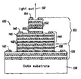
optical pick-up. As indicated with arrow 132, the device 130 emits light from
its top.
The device 130 is constructed on a GaAs substrate 134. An n-doped bottom
minor stack 136 includes 26 pairs of AIAs/AIo,SGao.&SAs DBRs, followed by 10
pairs
of AIo.,Gao.,As/Alo.,SGao.gSAs L)BRs, and a 3~./4-thick Alo9gGaflo,As
oxidation layer
I38 that is one pair away from the active region 142. The n-doped bottom minor
stack
I36 also includes a bottom n-contact 140.
The undoped active region 142 is composed of three 70-~ GaAs quantum wells
with 100-~ AIo.,SGaa gSAs barriers all within a 1-.1 spacer.
The p-doped mirror stack 144 includes a p-doped 3~./4-thick Alo.9gGao.o,As
oxidation layer 145 that is one pair away from the active region 142. The
stack 144
also includes S pairs of p-doped Alo,9Gao,As/GaAs and 4 pairs of P+doped
Alo.9Ga9,,As/AIo.,SGaflgSAs for 'the p-contact 146.
The device 130 also includes an optical absorber 150, also referred to herein
as
a
a quantum well absorber or modulator 150. The absorber 150 includes a 90-A
GaAs
undoped quantum well absorber with 90-~1 AIo,SGafl.85As barriers all within a
5~,/4
16
CA 02330537 2000-10-27
WO 99/57789 PCT/US99/09607
spacer, with the quantum well positioned 3~./4 of the way into the spacer from
the
substrate side.
An n-doped top mirror stack 152 is at the top of the device 130. This stack
may be implemented with 19.5 pairs of n-doped
Alo.9Gao,As/AIo,,SGa°.$SAs. The stack
1 S2 includes a top n-contact 154.
The described n-p-n dewice 130 may be considered to comprise a bottom DBR
stack 136 and a top DBR stack 160, which includes the active region 142, p-
doped
mirror stack 144, optical absorber 1 S0, and n-doped top mirror stack 1 S2.
The p-n
junction between the bottom stack 136 and the top stack 160 serves as the
active
element or gain element 142. The top n-p junction (between p-doped mirror
stack 144
and n-doped top mirror stack 1 S2) serves as the voltage controlled optical
absorber
150.
The optical absorber 150 has been placed at an optical intensity peak within
the
DBR stack, resulting in high impact on the device output for a small
modulating
voltage. The absorber 150 consists of a spacer (at least 31/4 thick)
containing one or
more quantum wells placed at a peak of the optical field intensity at the
Fabry-Perot
wavelength. The absorbing quantum wells' absorption edge should be positioned
so
that a zero applied voltage bias, the Fabry-Perot wavelength (~,Fp) is longer
or redder
than the absorption edge (~,aes). This wavelength difference depends on the
quantum-
well composition. The Fabry-Perot wavelength should be positioned so that it
overlaps with the tail of the quantum-well absorption spectrum at zero bias,
but when a
non-zero bias is applied (causing the absorption edge to shift towards longer
wavelengths), the excitonic peals should still be prominent enough when it
sweeps
through the Fabry-Perot wavelength. The optical absorber 150 may also be
2S implemented at off peak positions.
The device 130 has been implemented with a bottom mirror reflectivity of
99.995% at 8S2 nm, the intended Fabry-Perot wavelength ~,FP. The top mirror
reflectivity without absorption is designed to be 99.89% at ~.FP. By assuming
a loss of
S000crri' in the absorber quantum well, the top mirror reflectivity drops to
99.68% at
8S2 nm, enabling the laser to turn-off.
To establish self pulsation, the device is designed with the Fabry-Perot
wavelength longer than the absorber band-edge (~.Fp > nabs) in order to obtain
negative
17
CA 02330537 2000-10-27
WO 99/57789 PCT/US99/09607
differential resistance in the absorber. fhe device is biased using the
circuitry shown
in Figure 20. As discussed below, the DC absorber bias loads. R and Vo, are
chosen
such that the operating load line is tangential to the absorber hVa trace, as
shown in
Figure 38. This operating condition leads to controllable self pulsation of
the device.
By simply varying the electrical bias conditions, the user can turn the self
pulsations
on and off and can tune the frequency at which the self pulsations occur.
Furthermore,
because the device is designed (~,Fp > dabs) to obtain very sharp negative
differential
resistance in the absorber, self pulsation can be obtained at high laser
powers using a
small absorber bias.
Figure 20 illustrates a circuit used to establish self pulsation in the device
130
of the invention. The optical absorber 150 of the device 130 is biased with a
voltage
source, producing voltage Vo in series with a variable resistor R, as shown in
Figure
20. A termination path is provided for any generated AC signal in the
absorber. The
circuit of Figure 20 allows the user to control the device operating point in
order to
achieve self pulsation, bistabili.ty, or normal lasing. Node 170 of the
absorber junction
(the end that is shared by the g~sin region) is grounded. Node I72 is attached
to a bias-
T circuit 174 with a first branch including a capacitor C in series with the
50-Ohm
resistor to provide a path for the generated AC signal, and a second branch
including
an inductor L in series with a potentiometer (producing variable resistance R)
and a
DC voltage source producing voltage Vo. R and Vo are adjusted so that the load
line
for the absorber junction is tangent to the region of negative differential
resistance.
Figure 21 illustrates a dlriving circuit that may be used to modulate the
device
130. The absorber 150 is reverse biased with a DC voltage source. The AC
signal to
the absorber is superimposed on the DC signal through the previously described
bias-T
circuit. The p-contact 146 sen~es as the common ground for both the absorber
150 and
the active region 142. A DC current source is used to pump the active region
142, and
a 5052 termination path is provided for any AC signal generated in the gain
region.
Figure 22 illustrates the; L-I,~e~ and I,~~ V,a~~ characteristics of an
embodiment
of the invention. The threshold current is 1.7 mA. The threshold voltage is
5.6 V as
measured with injection between the p-contact 146 and the bottom n-contact
140. The
output power typically peaks at 0.7 mW. When the absorber is on {e.g., Vo 2V),
the
threshold current does not change appreciably since the threshold current
density of
18
CA 02330537 2000-10-27
WO 99/57789 PCT/US99/09607
approximately 2kA/cm'- is already fairly high due to the mismatch of ~.Fp and
the gain.
However, the differential quantum efficiency tad depends more strongly on the
minor
loss and hence decreases with iincreasing absorber reverse bias (r)d drops by
0.2% for
tlVo=2V; peak power decreases by 20%).
Figure 23 illustrates the: device response to absorber modulation under
several
DC bias conditions (I,~~~) for the gain region. The experimental results
indicate a -3-
dB small-signal bandwidth of 9GHz at I,~~ 8 mA with 0.6% modulation depth. The
bandwidth as well as the relaxation oscillation frequency increase with laser
bias
current I,~«, as expected in conventional modulation. This functional
dependence is
shown in Figure 24.
The absorber modulation response for fixed laser bias currents at different DC
absorber biases was measured. Figure 25 illustrates that the bandwidth does
not
change appreciably with varying absorber DC bias.
The absorber modulatic>n technique of the invention effectively modulates the
minor loss since the absorber is part of the VCSEL mirror stack. The minor
loss
modulation in turn leads to modulation of the photon lifetime.
One design criterion for the device of the invention is the relative placement
of
three wavelengths: the gain (~.sa;~), the absorber (~.abs), and the Fabry-
Perot transmission
peak (~,Fp). Ideally, for maximum overlap of the gain peak Wlth ~.FP, it is
desirable to
have /~,Ba;n < /~.FP to account for the red-shifting of the gain peak with
increasing pump
current and consequent heating,. At the same time, the absorption edge of the
quantum-well modulation should be positioned so that a small change in the
applied
voltage across the absorber induces a large change in the absorption. This
requirement
leads to the condition that 7~ebs '< .1FP, but with these two wavelengths
fairly close.
Since the wavelength of the voltage-biased absorber will not shift as
drastically as that
of the pumped gain region, the ideal relative positioning of the three
wavelengths
should then be ~lga;~ < ~.abs ~ fFP
If ~,abs < ~,FP is much too long compared to the gain or absorber, more
voltage
across the absorber is required to shift the absorption edge and obtain
modulation.
This leads to poor modulation efficiency. Also, the small overlap of the gain
peak
with ~,FP results in small bandwidth.
19
CA 02330537 2000-10-27
WO 99/57789 PCT/US99/09607
A large modulation depth can be achieved by aligning the Fabry-Perot
wavelength to be redder than the absorber quantum-well band edge. This will
result in
excellent modulation depth with this absorber modulation technique. A reverse
bias
across the absorber can then be used to sweep the absorption edge across the
Laser
emission, resulting in a very high on-off ratio.
Figure 26 illustrates output power as a function of bias current. A noticeable
discontinuity in dL/dIg and a hysteresis loop are observed at threshold,
indicating
bistable operation. As the absorber bias voltage and resistance are varied,
the
hysteresis loop can be made tC~ close as shown in the figure, and the laser
begins to
self pulsate. The transition between bistability and self pulsation can also
be
explained using the absorber I;,-Ve characteristics in Figure 27. If R and Vo
are
adjusted so that the load line crosses the absorber I; Va three times, then
bistability is
observed. As the load line is tilted so that it matches the negative slope of
Ia-Va more
closely, the system enters a state of instability and self pulsations
commence. The
typical threshold of a 25 p.m aperture self pulsating laser occurs at
approximately
8.5mA with a voltage across the active region of approximately 3.3 volts and a
peak
output power of approximately 1.5 mW.
The foregoing discussion demonstrates the importance that negative
differential resistance (NDR) ~~ssumes in the operation of the invention. The
negative
differential resistance (NDR) exhibited by the absorber Ia Va traces account
for the
unusual behavior of this device. If the absorber bias (R and Vo) is adjusted
so that the
operating load line intersects a single absorber Ia-Va trace three times, then
the device
operates in a bistable manner. If instead the load line is tangential to the
region of
negative differential resistance: in an absorber Ia-V~ trace, then the device
operates in an
unstable state; this is the regime of self pulsation. The device is designed
to obtain
regions of sharp negative differential resistance in the absorber Ia-Va
characteristic so
that relatively low absorber biases (e.g., R = 10 to 100 kW, Vo= 5 to 5 V) are
required
to obtain self pulsation.
To ascertain whether self pulsation can be achieved, the current-voltage (Ia
V,)
trace for the absorber was measured. Negative differential resistance (NDR)
was
obtained over a range of laser bias currents as shown by the Ia Va
characteristics of a
typical saturable absorber in Figure 27. The absorber current is proportional
to the
zo
CA 02330537 2000-10-27
WO 99/57789 PCT/US99/09607
applied electric filed across the: absorber junction and the optical power.
When the
absorber is forward biased, it behaves as a normal diode. As the absorber
reverse bias
increases (at the same laser bias), two competing processes affect the
absorber current.
The electric field causes the current to increase, whereas the increased
absorption
S reducing the laser power causes the absorber current to decrease. For small
Va, the
former effect dominates, while for large Va, the latter effect is stronger.
When the
reverse bias voltage increases durther, the absorption of the absorber
junction is too
great and the VCSEL stops lasing. The resultant drop in the optical power
causes the
absorber current to drop and approach the value determined solely by the
applied
electric field. The NDR appears in the region where the absorber current
decreases
with increasing reverse bias.
The operation of the device of the invention is also impacted by quantum-well
sub-bands of the absorber 150, as reflected in the fine features in the Ia Va.
These
features can be described as follows. The NDR is enhanced by strategic
placement of
the absorber and Fabry-Perot wavelengths. The absorber spectra for different
reverse
bias voltages are sketched in Fiigure 28 as a function of wavelength. The
vertical
arrow shows the position of thc; laser emission (~,i,~~~g), which is fixed
when the laser
bias current is fixed. Point a indicates the amount of absorption at ~,,es~~s
when V', _
V,. When the reverse bias is increased to V,, the absorption and hence the
absorber
current increase as the quantum-well absorption edge red-shifts, as shown by
point Vii.
When Ve is increased sufficiently, then the absorption decreases to point y,
bringing
the absorber current back down to a mostly constant value. Thus, the strategic
placement of the Fabry-Perot vvavelength and the quantum-well absorption edge
significantly enhances the NDR, providing flexibility in the design for self
pulsations
or bistability.
Self pulsation was measured using a high-speed detector and an RF spectrum
analyzer. The non-self pulsating state is shown in Figure 29(a) under
conditions of
stable operation. The trace essentially depicts relative intensity noise as
the device
behaves as a conventional laser. Figure 29(b) shows a trace of the self
pulsation
centered at 1.86 Ghz with a FVh/HM (-3dB) of at most 10 Mhz for the laser bias
current
set at IK = 9 mA, the saturable absorber bias voltage at Vo = 2 V, and the
variable
resistor at R = I 0 k12.
21
CA 02330537 2000-10-27
WO 99/57789 PCT/US99/09607
Figure 29(c) shows the self pulsation frequency at 1.34 Ghz with R = 75 k~2
and Vo = 6 V for a laser bias current of 6 mA. Likewise, the self pulsation in
Figure
29(d) occurs at R = 100 kS~ ands Vo = 10 V for a laser bias current of Is =
5.5 mA with
the frequency at 1.1 Ghz.
Figure 30 shows a plot of the self pulsating frequency as a function of the
laser
bias current Ig. This frequency can be tuned by adjusting the laser bias
current Is as
well as the saturable absorber circuit parameters (i.e. Vo and R).
The device of the invention can be used for optical pick-up detection. For
example, the device can be used as an integrated optical disk readout device
that
provides a low noise, compact ~~Iternative to existing bulk edge-emitter and
external
photodetector readout schemes. The negative differential resistance discussed
in
connection with self pulsation i,s required to obtain the bistability
necessary for this
function. Bistable laser output is achieved by choosing R and Vo such that the
load
line crosses the absorber I-V (ceurrent-voltage) trace three times (hence two
stable
1 S solutions and one unstable one). The absorber biases R and Vo are chosen
to minimize
the width of the hysteresis loop in the L-Is trace while maximizing the
magnitude of
the discontinuity in dL/di.
Optimal, efficient pick-up detection means that a small change in the photo-
generated absorber current results in a large change in absorber voltage.
Therefore, the
load line and hence the slope of the negative differential resistance needs to
be fairly
steep as in the case of self pulsation. The use of quantum wells and their
excitonic
peaks in the absorber allows for such a feature.
Current optical disk readout schemes use an edge-emitting laser as the optical
source and a separate external photodetector. The present invention integrates
the
optical source and detector into a single device. This approach eliminates
noise due to
reflections from unnecessary bulk optics and also minimizes the physical size
of the
device. Furthermore, the circular beam output allows the output beam to be
focused to
a spot size which is smaller than that of an edge-emitting device. Focusing
the beam
to a smaller spot size increases the allowable information density on the
optical disk.
The vertical-cavity geometry allows for possible use of two-dimensional
arrays, which
allows for parallel readout. The two-dimensional nature of VCSELs also means
22
CA 02330537 2000-10-27
WO 99/57789 PCT/US99/09607
wafer-scale fabrication, resulting in high device yield as well as high device
density on
each wafer.
Figure 31 (a) illustrates the device of the invention configured for optical
pick-
up. Figure 31 (a) shows bias circuitry 180 that rnay be used in an optical
pick-up
application. The absorber 1 SO is biased in parallel with a capacitor C (e.g.,
C=0.2pF)
and an inductor L (e.g., L=1013). Only DC current can flow through the branch
with
the inductor L; while only AC' current can flow through the branch with the
capacitor
C. A DC voltage bias Vo (e.g.., Vo = 9V) and a resistive load R, (e.g., R_,--1
l2kfZ) are
placed in series with the inductor L. A second resistor R, is placed in series
with the
absorber 150. The combined .load R, + R, and Vo determine the DC bias
conditions
for the absorber; R, + R, and 'Jo are chosen such that the operating load line
intersects
the absorber current-voltage (l-V) trace three times in order to obtain
bistable device
operation. The AC current generated in the absorber flows through R, and the
branch
with the capacitor to ground, resulting in a time-variation in the measured
voltage Va
which is proportional to the magnitude of the AC current.
Figure 31 (b) shows the; optical cavity used with the device of the invention
in
order to perform optical pick-up. Light emitted by the device 130 is focused
with a
series of collimating and focusing lenses 182 onto an optical disk 184. The
light
reflected from the optical disk 184 is then focused back onto the device 130.
through
the same series of lenses 182. The intracavity absorber 150 integrated into
the device
130 responds to the reflected light with a time-varying absorber current,
which is
measured using the device circuitry described above.
To perform optical disk read-out, the device is biased using the circuitry
shown
in Figure 31 (a) and is placed inn the external optical cavity shown in Figure
31 (b). A
DC gain bias is applied to the device so that the device lases, and the output
light is
tightly focused onto the optical disk 184 to be read. The optical disk 184
reflects
varying amounts of optical power, which is then focused back onto the device
130
through the same series of lenses 182. The intracavity absorber in the device
responds
to the varying optical power with a varying absorber current Ia, resulting in
a
measurable variation of the absorber voltage Va, which functions as the
optical pick-up
read-out signal.
23
CA 02330537 2000-10-27
WO 99/57?89 PCT/US99/0960?
In order to amplify the variation in the absorber current and hence in the
read-
out signal, the device and biasing circuitry are designed as follows. The
device is
designed so that the Fabry-Perot wavelength is longer than the absorber band-
edge and
hence the intracavity absorber exhibits negative differential resistance, as
shown in
Figure 36(b). The DC absorber bias circuit is configured so that the operating
load
line for the device intersects the absorber current versus voltage (I8 Va)
trace three
times, as shown in Figure 37. This causes the device to operate in a bistable
manner,
as shown in Figure 32. The absorber biases R and Vo are chosen to minimize the
width of the hysteresis loop in the L-I~ trace while maximizing the magnitude
of the
discontinuity in dL/dIg. The I)C gain bias current Ig is set to the value at
which the
variation in the absorber current with and without optical feedback is
maximum; this is
Point C in Figure 33. This technique causes a dramatic amplification of the
readout
signal.
Figure 32 shows the dcaired L-I~ trace, under typical bias conditions of R =
1 S 20kS2 and Vo = 4 V. As illustrated in the figure, when optical feedback is
provided by
the external cavity, the L-Ig trace shifts upwards, indicating that optical
switching has
occurred.
Figure 33 shows that the optical switching is accompanied by a switching of
the voltage Va across the integrated absorber. The laser bias current Is is
chosen such
that the VCSEL operates at the point C marked in the figure. This operating
point
maximizes the magnitude of the switching in the absorber voltage. The absorber
I; Va
traces with and without feedback and the load line corresponding to the bias
conditions
R = 20kk~2 and Vo = 4V are shown in Figure 34. From the intersection points of
the
load line with the I; Vas, one c;~n predict an absorber voltage and current
swing of O.SV
and 24wA, respectively, when optical feedback is applied under these bias
conditions.
Experimental measurements of this voltage and current swing are virtually
identical to
the quantities predicted by the load line.
Figure 35 demonstrates the operation of the device of the invention under bias
conditions of R=180ks2, Vo 9'V, and I6 2.SmA. As the feedback is switched on
and
off at a rate of 2.5 kHz, the volitage across the absorber varies by 220mV
with very low
noise. Thus, the device functions well as a compact, integrated optical disk
readout
device.
24
CA 02330537 2000-10-27
WO 99157789 PCT/US99/09607
In conclusion, the placement of the Fabry-Perot wavelength (~.FP) relative to
the
absorber band-edge (~.ebs) is cmcial to the various device manifestations
discussed. In
order to obtain an integrated deaector with accurate power tracking, ~.FP is
set less than
Webs. With this design, the intracavity absorber behaves like an integrated
S photodetector, with a linear response to applied optical power, as shown in
Figure
36(a). To establish negative differential resistance (NDR) in the intracavity
absorber.
~,Fp is set larger than ~.abs. The response of the absorber with this design
is shown in
Figure 36(b). This NDR can b~e utilized to obtain different device operations
depending on how the absorber is biased. If the load line, which is determined
by the
DC absrober bias (R and Vo; see Figures 20 and 31), crosses the absorber
current-
voltage (Ia V~ characteristic trace three times, as shown in Figures 37,
bistable
operation is established, which can ne used for optical pick-up. If the load
line is
tangential to the absorber Ia-Va trace in the region of NDR, as shown in
Figure 3~, then
self pulsation is obtained.
The foregoing description, for purposes of explanation, used specific
nomenclature to provide a thorough understanding of the invention. However, it
will
be apparent to one skilled in the art that the specific details are not
required in order to
practice the invention. In other instances, well known circuits and devices
are shown
in block diagram form in order to avoid unnecessary distraction from the
underlying
invention. Thus, the foregoing descriptions of specific embodiments of the
present
invention are presented for purposes of illustration and description. They are
not
intended to be exhaustive or to limit the invention to the precise forms
disclosed,
obviously many modifications and variations are possible in view of the above
teachings. The embodiments vrere chosen and described in order to best explain
the
principles of the invention and its practical applications, to thereby enable
others
skilled in the art to best utilize the invention and various embodiments with
various
modifications as are suited to the particular use contemplated. It is intended
that the
scope of the invention be defined by the following Claims and their
equivalents.
2S