Note: Descriptions are shown in the official language in which they were submitted.
CA 02330862 2003-02-10
_1-
BROADBANT> DIFFRACTIVE DIFFUSER AND ASSOCIATED METHODS
Field of the Invention
The present invention is directed to diffractive diffusers, in particular to
broadband
diffractive diffusers.
L7escription of Related Art
A binary or d,iffractive diffuser functions well as its design wavelength? but
suffers
significant contributions from the zero-order as the wavelength deviates from
the
design wavelength. The zero-order contributions arise from that light which is
not
diffracted. This will lead to undesirable peaks in intensity when the design
wavelength is deviated frown.
A schematic view of a prior art binary diffuser is shown in Figure 1. In
Figure 1,
a binary or diffraetive diffuser lU consists of amorphous, free-form regions
roughly
evenly split between regions presenting a zero phase shift and regions
presenting a ~
phase shift to incoming light. These regions are so labeled in Figure 1. These
regions
are formed the different etching depths shown in the prior art of Figure 2.
The zero
regions are not etched at all, while the n regions are etched to a depth of
d~, where
dl=~,,o/2(n-1 ), wh<~re ~,.~, is the design wavelength and n is the index of
refraction of the
diffuser. Thus, at the design wavelength, the etched portions present a phase
shift of ~
or ~,a/2 to the incoming light.
CA 02330862 2003-02-10
-2-
Light at different wavelengths will interact with the diffuser 10 as shown in
the
phasor histograms in prior art Figures 3a-3c. When an input wavelength ~, is
the design
wavelength a.~,, the Zero order contributions from the zero regions and the ~r
regions
cancel each other, thereby resulting in no zero order contribution, as shown
in Figure
3a. When the input wavelength i~ is less than the design wavelength, as shown
in Figure
3b, for the phase shift of zero, ~h~ zero order contribution will be the same
as that for
the design wavelength, i.e., zero. However, for the portions etched to the
depth of d~,
this depth will no longer look like a phase shift of n to the input
wavelength, but rather
a phase shift of greater than n. '1'he resultant vector 12 has an amplitude of
sin'[(ac/2) l,~l i~ -1)]. Similarly, when the input wavelength i~ is greater
than the design
wavelength, as shown in Figure 3c, the portions etched to the depth of d~ will
present a
phase shift of less than rc, with a resultant vector 14 having an amplitude of
sinz ((n12)
(~o/ 7~ _1)).
The shift of the phasor vector for the ~ phase shift regions away from the
axis so as
to cancel the contribution from the zero phase shift regions reduces the
efficiency of
the diffuser 10 at wavelengths other than the design wavelength. For example,
in the
range of ~, _ .83 ~,o to ~, = 1.2ia 7~0, the zero order diffraction efficiency
will be as high
as 10%, i.e., 10% of the input beam will be delivered to the zero order,
severely
reducing the efficiency and general usefulness of the diffuser 10.
CA 02330862 2003-02-10
-3-
Summar~r of the Present Invention
Therefore, it is an object of the present invention to provide a diffractive
diffuser
that is less sensitive to deviations from a design wavelength, i.e., a
broadband
diffractive diffu;>er.
It is further an object of the present invention to provide a diffractive
diffuser
having at least three discrete levels. At least tow of the levels may have a
phase
difference of approximately n between them.
It is further an object of the present invention to provide a broadband
diffractive
diffuser including a computer generated hologram designed at a wavelength ~,o
for
which light of a wavelength ~. incident thereon has a total power in a zeroth
order of
less than sinz((~:/2)(~,°/ ~. -l;)). Such a diffuser may, for 0.837~a'~
~. $ 1.20,0, have a
zeroth order be sin4((~/2)(~.,~/ ~. -1)).
It is an additional object of the present invention to provide a broadband
diffractive
diffuser including a computer generated hologram designed at a wavelength ~,o
for
which light of a wavelength ~,, 0.83.0 <_ ?~ $ 1.20.0 , incident thereon has a
zero order
diffraction efficiency of less than i%.
It is another object of the present invention to provide a diffractive
diffuser
including a plurality of rel;ions, approximately 50% of an area of the
plurality of
regions presenting a phase shift of ~ at a design wavelength, approximately
25% of the
area of the plurality of regions presenting a phase shift of ?~ at the design
wavelength,
and approximately 25% of the area of the plurality of regions presenting a
phase shift
of 0.
CA 02330862 2000-10-30
WO 99/575$3 PCTNS99/09704
It is further an object of the ;present invention to provide a diffractive
diffuser
having a plurality of regions designed to operate at a design wavelength,
while the
diffractive diffuser provides iiglht at a wavelength other than the design
wavelength
with more than two phasor vectors at zero order.
It is further an object of the lpresent invention to provide a method of
designing a
broadband diffractive diffuser. The method includes generating a diffractive
diffuser
pattern at a design wavelength and modifying the diffractive diffuser pattern
to
provide light at a wavelength other than the design wavelength with more than
two
phasor vectors at zero order.
The modifying may include generating a different diffractive diffuser pattern
at the
design wavelength and performiing a logical operation between regions of the
diffractive diffuser pattern which present a zero phase shift with the
different
diffractive diffuser pattern. The generating of the different diffractive
diffuser pattern
may include rotating the diffractive diffuser pattern. The logical operation
may be an
AND operation.
Alternatively, the modifying may include generating a different diffractive
diffuser
pattern and adding phases of said different diffuser pattern to corresponding
phases of
the diffractive diffuser patter. This adding may include the diffractive
diffuser pattern
forming an undersized desired output, the different diffractive diffuser
pattern forming
a spot, and a modified pattern farmed by adding phases of the different
diffractive
diffuser pattern and the diffractive diffuser pattern generating a desired
output.
CA 02330862 2000-10-30
WO 99/57583 PCT/US99/09704
-5-
Alternatively, the generating may include splitting the diffuser into regions
having
a phase shift of ~ and regions having a phase shift of zero at the design
wavelength,
and the modifying may include splitting regions having a phase shift of zero
into
regions having a phase shift of ;zero and regions having a phase shift of 2~c
at the
-5 design wavelength. At least one; of the splittings may be even. At least
one of the
splittings may result in amorphous regions. The splittings may include a pixel-
by-pixel
search.
In accordance with the above objects, the plurality of regions may have an
amorphous shape. The plurality of regions may be formed by a computer-
generated
hologram.
Further scope of applicability of the present invention will become apparent
from the
detailed description given hereinafter. However, it should be understood that
the detailed
description and specific examples, while indicating preferred embodiments of
the
invention, are given by way of illustration only, since various changes and
modifications
i 5 within the spirit and scope of the invention will become apparent to those
skilled in the
art from this detailed description.
Brief Description of the Drawings
The present invention will become more fully understood from the detailed
description given hereinbelow and the accompanying drawings which are given by
way
of illustration only, and thus are not limitative of the present invention,
and wherein:
CA 02330862 2000-10-30
WO 99/57583 PCT/US99/09704
-6-
Figure 1 is a schematic illusihration of a related diffractive diffuser;
Figure 2 illustrates the etch depth for the diffractive diffuser shown in
Figure 1;
Figure 3a is a phasor histogram of the zero order contribution for the
diffractive
diffuser shown in Figure 1 at the design wavelength;
Figure 3b is a phasor histogram of the zero order contribution for the
diffractive
diffuser shown in Figure 1 for wavelengths less than the design wavelengths;
Figure 3c is a phasor histogram of the zero order contribution for the
diffractive
diffuser shown in Figure 1 for v~~avelengths greater than the design
wavelengths;
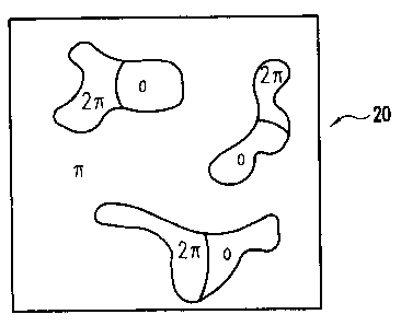
Figure 4 is a schematic diagram of a broadband diffractive diffuse element in
accordance with the present invc;ntion;
Figure 5 illustrates the etch dlepths for the diffractive diffuse of Figure 4;
Figure 6a is a phasor histogr:nn of the zero order contribution for the
diffractive
diffuser shown in Figure 4 at the; design wavelength;
Figure 6b is a phasor histogram of the zero order contribution for the
diffractive
diffuser when the input wavelength is less than the design wavelength; and
Figure 6c is a phasor histogram of the zero order contribution for the
diffractive
diffuser shown in Figure 4 when the wavelength is greater than the design
wavelength.
Detailed Description of the Preferred Embodiments
Figure 4 is a schematic diagram of a diffractive diffuser 20 in accordance
with the
present invention. As can be seen therein, the zero regions have been
subdivided into
subsets of zero and 2n. While in Figure 4, the previously zero regions have
been
CA 02330862 2000-10-30
WO 99/57583 PCT/US99/09704
roughly divided in half to split between the zero and 2n regions, these
regions may be
subdivided in many ways as long as over entire surface approximately 50% of
the
surface presents a phase shift of ~ to the design wavelength, approximately
25% of the
surface presents a phase shift of zero to the design wavelength, and the
remaining 25%
of the surface presents a phase shift of 2~ to the design wavelength.
The etch depths for the diffi-active diffuser 20 are shown in Figure 5. Again,
d,=7~/
2 (n -1 ) while the additional depth d2=~,~/ (n -1 ). Thus, the design
wavelength, the
depth d2 presents a phase shift of 2n and the depth dl presents a phase shift
of ~. At
the design wavelength, a phase shift of zero and a phase shift of 2n are
mathematically
identical. Thus, the diffracdve diffuser 20 will function identically to the
diffractive
diffuser 10 at the design wavelength. However, the inclusion of the phase
shift 2~ at
the design wavelength will result in a third vector of the zero order
contribution for
wavelengths other than the design wavelength. This third vector, when summed
with
the other vectors arising from the phase shift of zero and the phase shift of
~t, will
reduce the amplitude of the resultant vector. This is shown in Figures 6a
through
Figures 6c.
As can be seen in Figure 6a, the zero order contribution when the input
wavelength
is the design wavelength is still zero, since the phase shift of zero and 2n
will look the
same at the design wavelength. As shown in Figure 6b, when the input
wavelength is
less than the design wavelength, there will be a third phasor vector arising
from the
presence of the 2~ portions. The resultant vector 22 will have an amplitude of
sin4((n
/2) (~,~/ ~, -1)). Thus, the zero order contribution will be significantly
reduced from
CA 02330862 2000-10-30
WO 99/57583 PCT/US99/09704
_g_
that previously shown in Figure; 3b. Similarly, in Figure 6c, the resultant
vector 24
will have an amplitude of sin4((~/2 )(7~/ ~, -1)). For the range noted
previously of
~,=.83 ~.o through ~, = 1.20 ~,o, the zero order diffraction deficiency is
reduced to less
than 1 %. Thus, the magnitude of the zero order contribution of the diffuser
20 for the
S non-design wavelengths is reduced by an order of magnitude compared with the
diffuser 10.
The diffuser 20 of the present invention may advantageously be produced by
generating two patterns for a diffuser as shown in Figure 1 and then logically
combining these patterns. Morf; specifically, a first diffractive diffuser
pattern is
generated and a second diffractive diffuser pattern is generated and
superimposed on
the first pattern. The zero regions of the first generated pattern may then be
subjected
to, for example, an AND operation with the second generated pattern to form
the
regions of zero and 2n. For example, when ANDing the two patterns, when both
regions are zero, that region will remain a zero region, when both regions are
~
regions, that region will remain a ~ region, but if the region is zero in one
pattern and
n in the other pattern, that region will become a 2~ region. Of course logical
operations may be performed mathematically using functions describing the
respective
patterns.
As an example, a single pattern as shown in Figure 1 is generated, and then
this
pattern is rotated by 90E and used as the second generated pattern. The single
pattern
is generated in accordance with a desired distribution over a desired region
of a
CA 02330862 2000-10-30
WO 99/57583 PCT/US99109704
-9-
desired shape at the design wavelength. These two patterns are then ANDed to
form
the pattern having the three phase regions distributed thereon.
Another method using two patterns involves adding the phases in corresponding
regions in two binary patterns. In this method, where both patterns are 0, the
final
pattern has a phase of 0, when both are n, the final pattern has a phase of
2~, and
where one pattern is 0 and one its ~, the final pattern has a phase of ~c. The
final or
resulting pattern in the input plme is the Fourier Transform pattern of the
desired
output. The addition of the phases in the input plane, which is the spatial
domain,
results in the convolution of the pattern in the output plane, which is the
frequency
domain. Thus, when adding the; phases within two patterns, these patterns are
designed to account for the fact that their respective outputs will be
convolved.
For example, a first pattern may be generated in accordance with the desired
output
at the design wavelength, but having an output that is slightly smaller than
the desired
output. The second pattern is then generated to form a small spot in the
output plane.
1 S When the phases of this second pattern are added to the phases of the
first pattern, the
resulting pattern has 0, ~ and 2~; regions, and the resulting output is larger
than the
output of the first pattern, thereby forming the desired output. Thus, the
first and
second patterns are designed in relation to one another so that the second
pattern
increases the size, or blurs, the first pattern to form the desired output. In
this example,
the first pattern contains the high frequency information needed to generate
the desired
output, while the second pattern contains the low frequency information needed
to
generate the desired output.
CA 02330862 2003-02-10
-10-
An alternative manner of zero-order balancing the broadband diffuser 20
involves
a fractal method of splitting the zero regions into regions of zero and 2n. A
single
diffuser pattern is generated, then searched to determine regions where the
phase is
zero. This search involves scanning every pixel in the pattern until a pixel
with zero
phase is encountered. Then every pixel in this zero phase region is traversed,
e.g., in a
four connected fashion, e.g., examining the top, bottom, left and right pixels
adjacent
to the current pixel. This traversal proceeds until every zero phase pixel
that is
contiguously connected to the region is encountered. Each such zero phase
pixel is
flagged with an identifier indicating that it is part of the connected region.
T he
connected region is then traversed again from both sides, preferably starting
with the
first pixel and the last pixel encountered in the connected region. Pixels on
either side
are flagged with different identifiers until the region is divided
approximately in half.
One-half of the region is them set to have a phase of 2~c and the other half
is left having
the zero phase. This process is repeated for each zero phase region in the
original
diffuser pattern.
The initial diffuser patterns are formed as set forth in U.S. Patent
No. 5,850,300 issued 15 December 1998, in which a diffuser is to have a
desired fine width and the line widths are oriented randomly. These line
widths determine the angular region of the diffused beam in the far field.
The resulting computer generated pattern or hologram is a Fourier
Transform pattern that corresponds to the desired angular region. The
preferred method of generating such a pattern is using an iterative computer
optimization technique, such as the IDO method described in Iterative
Encoding-of
CA 02330862 2003-02-10
High Efficienc~~ Holograms f:~r Generation of Spot Arrays, Optics Letters,
Vel. I4, pp.
479-81, 1989. The resulting hcalogram may be constructed in known manners,
such as
set forth in U.S. Patent Nos. 4,895,790 and 5.,202,775.
The three different methi~ds set forth above for farming the diffractive
diffuser in
accordance with the present invention may result in a different final pattern
for the
broadband diffuser, buy all true final patterns should have three levels and a
phase
difference approximately equal to ~ between at least two of the levels.
Advantageously for the final patterns, approximately SO% of the surface
presents a
phase shift of ~ ~to the desigrx wavelength, approximately 2S"~o of the
surface presents a
phase shift of zero to the de:>ilm wavelength, and the remaining 25% of the
surface
presents a phase shift of 2n to the design wavelength.
The invention being thus, described, it will be obvious that the same may be
varied
in many ways. For example, the ~ regions may similarly be split into n regions
and 3~t
1 S regions, to reduce the resultant vector for non-design wavelengths. Such
variations
are not to be regarded as a ciepanture from the spirit and scope of the
invention, and all
such modifications as would ~be obvious to one skilled in the art are intended
to be
included within the scope of the following claims.