Note: Descriptions are shown in the official language in which they were submitted.
CA 02330970 2000-11-O1
WO 99/59047 ~ PCT/US99/10226
METHOD AND APPARATUS FOR
LOW JITTER CLOCK RECOVERY
s
The present invention relates generally to bus system architecture and,
more particularly, to a method and apparatus for reducing fitter in
isochronous
communications clock recovery.
io BACKGROUND
Today's consumer electronic devices are increasingly being
implemented as special-purpose computer systems, complete with processor,
memory, and v0 functionality. The various companies who design and manufacture
these devices may have their own particular interconnect technology and
~s communication protocols. Consequently, compatibility problems can occur
when
connecting devices made by different manufacturers. In home entertainment
systems,
for example, a DVD player manufactured by one company may be incompatible with
an audio speaker subsystem manufactured by another company.
To facilitate today's increasingly complex communication between
2o electronic devices, various standards have been developed. In particular,
the IEEE
1394 standard for a High Performance Serial Bus (also known as the "FireWire"
bus)
has been established to facilitate the development of compatible consumer
electronics
devices. In addition to defining a standard bus communications protocol, the
FireWire bus architecture also provides for standard connections, with each
2s interconnected device being able to communicate with every other such
device
without requiring individual point-to-point connections between the various
devices.
SUBSTITUTE SHEET (RULE 26)
CA 02330970 2000-11-O1
WO 99/59047 PCT/US99/10226
2
The IEEE 1394 standard (IEEE 1394-1995 and IEEE 1394a supplement) is entitled
"Standard for a High Performance Serial Bus," and is based on the ISO/IEC
13213
(ANSUIEEE 1212) specification, entitled "Informarion technology-Microprocessor
systems-Control and Status Registers (CSR) Architecture for microcomputer
s buses."
Referring to Figure 1, a typical home entertainment system 100 is
depicted. The system includes a high speed bus, such as an IEEE 1394 bus 102,
that
interconnects a variety of electronic devices. The particular configurarion
depicted is
intended solely to show the functional interconnection of representative
devices.
io Those skilled in the art understand that FireWire bus architecture supports
tree and
daisy chain connection configurations.
A DVD player 104 is included for playing DVD disks and
correspondingly outputting audio and MPEG video data streams on the 1394 bus
102.
The audio and video data streams are transported aver isochronous channels of
the
~s 1394 bus 102, with a surround sound decoder 106 receiving the audio data
stream
and a video decoder/monitor 108 receiving the MPEG video data stream. A cable
or
satellite set-top box 110 receives media from a cable or satellite television
provider
and outputs corresponding audio and MPEG video data streams on isochronous
channels of the 1394 bus 102. The surround decoder 106 receives the audio
data, and
2o the video decoder/monitor 108 receives the video data.
The surround sound decoder 106 receives compressed audio signals
from other devices connected to the 1394 Bus 102 and decodes the audio. The
decoded audio data is then output on the 1394 bus 102 to an amplifier/speaker
subsystem 112. The video decoder/morutor 108 decodes MPEG data streams
2s received from various video source devices on the 1394 bus 102. Once
decoded, the
SUBSTITUTE SHEET (RULE 26~
CA 02330970 2000-11-O1
WO 99/59047 PCTNS99/102Z6
3
uncompressed video signal is then typically output to a video monitor for
presentation.
A controller 114 provides a point of control for all devices in the
system 100. The controller 114 may also provide a user interface to configure
the
system when various devices are added or removed. The controller typically
includes
a user interface for adjusting audio volume, turning devices on and off,
selecting
channels on the set-top box 110, etc. Indeed, the controller may be the only
device a
user interacts with (other than inserting disks into the DVD player 104).
Each of the interconnected devices shown in the system 100 Figure 1
io includes interface circuitry connecting the 1394 Bus 102 to the particular
application
circuitry included in the devices. Such interface circuitry includes both the
physical
electrical connections (known as the PHY layer) and the data format
translation
interface (known as the Link layer). Such interface circuitry is well known
for those
skilled in the art, and the general features of such circuitry need not be
described
herein.
For video and audio applications, which require constant data transfer
rates, it is particularly important that a device receiving such data
accurately recover
the sample rate clock signal from the device transmitting such data. This
ensures that
data buffers in the system do not overflow or underflow. FireWire bus
architecture
2o supports transmission of isochronous data packets including time stamp
information
that can be used to recover the sample rate clock, such as in accordance with
the IEC
61883 standard, entitled "Digital Interface for Consumer Audio/Video
Equipment."
Because there is no requirement that different data streams be frequency
related (i.e.,
isochronous streams may have free-running sample rates), each receiving device
or
node must implement a separate clock recovery circuit for each received
isochronous
channel of the 1394 bus.
SUBSTITUTE SHEET (RULE 26)
CA 02330970 2000-11-O1
WO 99/59047 PCTNS99/10226
4
Referring to Figure 2, a functional block diagram depicts the prior art
approach of providing time stamps and correspondingly recovering a sample rate
clock. The interface circuitry included within a transmitting device or node
200 is
depicted, as is a portion of the interface circuitry included within the
receiving device
s or node 202. The transmitting node 200 includes a latch 204 that latches a
lower
portion of the value stored in a cycle time register 206 included within the
Link layer
of the interface circuitry. The latch 204 latches the cycle nme value every
predetermined number of cycles of the sample rate clock (such as a digital
audio
word clock in the case of audio data transmission). A transfer delay value is
added to
io the latched cycle time register value, and the resulting time stamp is
inserted into the
header of the corresponding isochronous data packet 208. As is known to those
skilled in the art, the value of the transfer delay is determined at system
initialization
or bus reset.
At the receiving device or node 202, the received time stamp is
is compared with the corresponding lower portion of the value stored in the
receiving
node's cycle time register 210. A comparator 212 produces a pulse signal in
the event
of equality, which is then input to a phase-locked loop (PLL) circuit 214 to
recover
the sample rate clock signal. All cycle time registers in a 1394 bus-based
system are
periodically set (at nominal 125 gs intervals) to the same value by a cycle
start
zo command issued by the the cycle master node, as is well understood in the
art. Each
node's cycle time register is then incremented by a quartz driven clock
circuit
included in the PHY layer of each node, with each clock circuit producing a
nominal
24.576 MHz clock signal. Figure 2 depicts PHY clock circuits 216 and 218 of
the
transmitting node 200 and receiving node 202, respectively.
2s The above-described approach of generating and receiving time stamps
has two particular problems associated with fitter. The first problem is that
the
separate PHY clock circuits included in each node may have slightly different
SUBSTITUTE SHEET (RULE 26)
CA 02330970 2000-11-O1
WO 99/59047 PGT/US99/10226
frequencies. The IEEE 1394 standard limits frequency deviations to 100 ppm
from
the nominal rate. Thus, the PHY clocks 216, 218 of the transmitting and
receiving
nodes 200, 202 could be off from one another by as much as 200 ppm. Over the
125~s isochronous cycle time, this translates to
s (200)*(24.576s'1)*(125~.s)=0.6144, or more than half a least significant
bit.
While the integer count is still essentially equal at the cycle time registers
206, 210 of
the transmitting and receiving nodes 200, 202, the instantaneous edges of each
register's shift can differ by up to 0.6144 of bit time, or
io (0.6144)/(24.576 MHz)=25ns.
Even with perfect phase-locked loop circuits in the rest of the clock recovery
circuitry, 25ns of fitter can occur.
The second problem associated with fitter arises from the finite length
nature of the generated time stamps and the resulting quantization noise. This
is quantization noise is correlated to the PHY clock circuit 216 and the
generated time
stamp period of the transmitting node 200. When the receiving node 202
recovers the
sample rate clock signal from the time stamp information, this clock is
jittered by the
quantization error. When this jittered clock is used to drive either a digital-
to-analog
or analog-to-digital converter, unwanted distortion is introduced into the
converted
2o audio signal and degrades signal quality.
SUMMARY
In accordance with the present invention, a method is provided for
recoverying sample clock signals. The method is performed in connection with a
SUBSTITUTE SHEET (RULE 26)
CA 02330970 2000-11-O1
WO 99/59047 PGTNS99/10226
6
system including an isochronous device, with the isochronous device having a
stored
cycle time value that is set by a periodic command issued at times referenced
to a
first clock signal. The method includes producing a second clock signal
referenced to
the first clock signal, and incrementing the stored cycle time value in
response to the
s second clock signal. A time stamp value is extracted from a data packet
received by
the isochronous device. The time stamp value is then compared to the stored
cycle
time value, and a pulse signal is produced in the event of a match. The
frequency of
the sample clock signal is then proportional to the frequency of successive
pulses.
The method may be performed in connection with an isochronous communications
io bus, such as an IEEE 1394 bus. In such case, the periodic command may be
the
cycle start command issued by the cycle master, with the first clock signal
being
produced by the cycle master. The second clock may then be referenced to the
incrementing of the cycle-count field of the stored cycle time value.
In accordance with another aspect of the present invention, circuitry is
~s provided for receiving a stream of data packets having associated time
stamp values.
The circuitry includes a buffer for receiving and temporarily storing the data
packets.
A packet parser is coupled with the buffer and separates the time stamp values
from
the data packets. A clock recovery circuit is coupled with the packet parser
and
compares the time stamp values to a cycle time value, with the clock recovery
circuit
20 then producing a data sample clock signal referenced to matched
comparisons. A
cycle time register is coupled with the clock recovery circuit and provides
the cycle
time value, which is set in response to a periodic command and incremented in
response to a clocking signal. A clocking circuit is coupled with the cycle
time
register and provides the clocking signal, which is referenced to the periodic
2s command. The circuitry may further include a phase-locked loop circuit that
drives
the clocking circuit, with the phase-locked loop circuit being referenced to
the
periodic command. The circuitry may be adapted for coupling with an
isochronous
SUBSTITUTE SHEET (RULE 26)
CA 02330970 2000-11-O1
WO 99/59047 PCTNS99/10226
7
communications bus, such as an IEEE 1394 bus. In such case, the periodic
command
may be the cycle start command issued by the cycle master, with the clocking
signal
then referenced to the incrementing of the cycle-count field of the stored
cycle time
value.
s In accordance with a further aspect of the invention, a method is
provided for generating a time stamp value referenced to a data sample clock
for
transmission with an isochronous data packet. The method includes latching a
cycle
time value at a time referenced to the data sample clock, adding a dither
value, and
filtering the result. The dither value may be determined according to a
triangular
io probability density function, and the filtering may include shifting noise
out of the
frequency range of the data sample clock.
In accordance with yet another aspect of the invention, circuitry is
provided for transmitting a stream of data packets having associated time
stamp
values. The circuitry includes a cycle time register that provides a cycle
time value.
is The cycle time value is incremented by a clocking signal provided by a
clocking
circuit. A data interface provides data and a corresponding data sample clock
signal.
A time stamp generator is coupled with the data interface and with the cycle
time
register. The time stamp generator produces the time stamp values by latching
cycle
time values at times referenced to the data sample clock, adding dither
values, and
2o filtering the resulting sum values. A packet generator is coupled with the
data
interface and with the time stamp generator. The packet generator combines the
time
stamp values with the data to form data packets. The circuitry may further
include a
packet buffer for temporarily storing data packets received from the packet
generator.
The packet buffer may be coupleable with an isochronous communications bus,
such
2s as an IEEE 1394 bus, for transmission of the data packets thereon.
SUBSTITUTE SHEET (RULE 26~
CA 02330970 2000-11-O1
WO 99/59047 PCT/US99/10226
8
BRIEF DESCRIPTION OF THE DRAWINGS
Figure 1 is a functional block diagram that depicts a typical IEEE 1394
system.
Figure 2 is a functional block diagram that depicts circuitry for
s producing time stamps by a prior art transmitting device and circuitry for
sample rate
clock recovery in a prior art receiving device in an IEEE 1394 system.
Figure 3 is a functional block diagram depicting a received isochronous
datapath through interface circuitry in accordance with an embodiment of the
present
invention.
io Figure 4 is a functional block diagram depicting a transmit isochronous
datapath through interface circuitry in accordance with another embodiment of
the
present invention.
Figure 5 is a functional block diagram depicting circuitry included in
the interface of Figure 4 for decorrelating and reducing noise in accordance
with an
~s embodiment of the present invention.
DETAILED DESCRIPTION
The following is a description of circuitry and methods for reducing
fitter in a recovered data sample clock. The circuitry and methods are
conformable to
the applicable IEEE 1394, ISO/IEC 13213, and IEC 61883 standards. In this
2o description, certain details are set forth in order to provide a thorough
understanding
of various embodiments of the present invention. It will be clear to one
skilled in the
art, however, that the present invention may be practiced without these
details. In
other instances, well-known circuits, circuit components, control signals, and
timing
and communications protocols have not been shown or described in detail in
order to
SUBSTITUTE SHEET (RULE 26)
CA 02330970 2000-11-O1
WO 99/59047 PCT/US99/10226
9
avoid unnecessarily obscuring the description of the various embodiments of
the
invention. The described subject matter relates to technology similar to that
disclosed in a concurrently filed patent application, entitled "Method and
Apparatus
for Data Sample Clock Recover," the disclosure of which is incorporated herein
by
s reference.
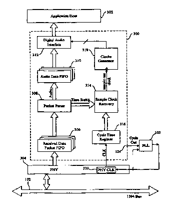
Figure 3 depicts an embodiment of the invention that addresses the
above-identified first problem associated with fitter in prior art approaches
to
isochronous communications. Figure 3 shows certain circuitry included within a
Link layer 300 of interface circuitry coupling the 1394 bus 102 to an
application host
io 302. The figure also depicts a physical/electrical interface or PHY layer
304. The
particular circuitry shown within the Link layer 300 is a simplified depiction
of the
datapath for received isochronous data, together with certain associated
control/monitor circuitry. Those skilled in the art will appreciate that a
wide variety
of circuitry is not shown in Figure 3, such as bus management layer circuitry,
~s transaction layer circuitry, datapath and control circuitry for transmitted
isochronous
data, and other link layer circuitry associated with asynchronous data
protocols.
Such well-known circuitry is not shown in order to avoid unnecessarily
obscuring the
description of embodiments of the present invention.
The Link layer circuitry 300 includes a FIFO 306 for receiving
2o incoming isochronous data packets, such as audio data packets. These data
packets
are passed on to a packet parser 308 that separates the audio data from the
header of
the packet, including the time stamp. The audio data is then passed on to
another
FIFO 310, and then on to the application host 302 via a digital audio
interface 312.
The packet parser 308 provides the time stamp values from the
2s isochronous data packets to a sample clock recovery circuit 314. The sample
clock
recovery circuit 314 includes circuitry like the comparator 212 and the phase-
locked
SUBSTITUTE SHEET (RULE 26)
CA 02330970 2000-11-O1
WO 99/59047 PCT/ITS99/10ZZ6
loop 214 described above in connection with Figure 2. The sample clock
recovery
circuit 314 produces a sample rate clock signal corresponding to the received
time
stamps and the value stored in a local cycle time register 316. This recovered
clock
signal is applied to a clocks generator circuit 318, which in turn provides
the various
s well-known clocking signals applied to the digital audio interface 312.
The cycle time register 316 is incremented in response to a local PHY
clock 320. Instead of being driven by a quartz crystal, as in the prior art,
the PHY
clock 320 is instead driven by a phase-locked loop (PLL) circuit 322 that is
referenced to a cycle-out pin 324 of the Link layer interface. As is known to
those
io skilled in the art, the cycle-out pin 324 toggles each time the cycle-
offset field
(lowest 12 bits) of the cycle time register wraps to zero (every 125 ~.s) and
the cycle-
count field (next 13 bits) is correspondingly incremented. Since the cycle-
count
interval equals the cycle master's cycle start command time interval, the
cycle-out pin
324 toggles at a rate proportional to the cycle master's clock (albeit with
the above-
is described jittery. Providing the PLL 322 with a sufficiently large loop
time constant
will then substantially filter out fitter and produce a clock signal of
substantially the
same frequency as the cycle master PHY clock. Even if the fitter is not
completely
filtered, an improved performance still results, since the jittery clock
signal produced
by the PLL-driven PHY clock will be statistically closer in frequency to the
cycle
Zo master than the prior art quartz-driven PHY clock. Although depicted as
external,
those skilled in the art will appreciate that the PLL 322 can be
advantageously
integrated within either the Link layer 300 or the PHY layer 304.
Each of the circuits described in connection with Figure 3 is of a type
well known in the art. One skilled in the art would be able to implement such
circuits
2s or their equivalent in the described or equivalent configuration to
practice the present
invention. Accordingly, internal and operational details of such circuits need
not be
provided.
SUBSTITUTE SHEET (RULE 26)
CA 02330970 2000-11-O1
WO 99/59047 PCTNS99/10226
11
Figure 4 depicts an embodiment of the invention that addresses the
above-identified second problem associated with fitter in prior art approaches
to
isochronous communications. Figure 4 shows circuitry included within a Link
layer
400 of interface circuitry coupling the 1394 bus 102 to an application host
402. The
s figure also depicts a physical/electrical interface or PHY layer 404. The
particular
circuitry shown within the Link layer 400 is a simplified depiction of the
datapath for
isochronous data to be transmitted via the 1394 bus 102, together with certain
associated control/monitor circuitry. Those skilled in the art will appreciate
that a
wide variety of circuitry is not shown in Figure 4, such as bus management
layer
io circuitry, transaction layer circuitry, datapath and control circuitry for
received
isochronous data, and other link layer circuitry associated with asynchronous
data
protocols. Such well-known circuitry is not shown in order to avoid
unnecessarily
obscuring the description of embodiments of the present invention.
The Link layer circuitry 400 includes a digital audio interface 406 that
~s receives incoming audio data from the application host 402 and passes this
data on to
a FIFO 408. This audio data is passed on to a packet generator 410 that
creates an
isochronous data packet, including the audio data and a time stamp. The data
packet
is passed on to another FIFO 412, and then transmitted via the 1394 bus 102 to
a
receiving device.
2o The packet generator 410 receives the time stamp values from a time
stamp generator circuit 414, which is discussed in further detail below. The
time
stamps correspond with values received from a local cycle time register 416 at
times
referenced to the audio sample clock signal received from the digital audio
interface
406. The cycle time register 416 may be clocked conventionally or as described
2s above in connection with Figure 3.
SUBSTITUTE SHEET (RULE 26)
CA 02330970 2000-11-O1
WO 99/59047 PCT/US99/10226
12
Figure 5 depicts certain circuitry included in the time stamp generator
circuit circuit 414. A time stamp is first produced by conventional time stamp
circuitry 500 similar to that described above in connection with the prior art
transmitting node 200 of Figure 2. A summation circuit 502 then adds the
s conventionally generated time stamp value to a dither signal, such as from a
triangular probability density function (TPDF) generator 504. As is known to
those
skilled in the art, dithering the time stamp decorrelates the fitter, at the
expense of
introducing broadband noise. Feeding back the summation circuit's output
through a
suitable noise shaping filter 506 then shifts this noise out of the expected
frequency
io band of the sample clock signal to be recovered. Remaining fitter power
will then be
further reduced during normal filtering done during clock recovery at the
receiving
node.
Each of the circuits described in connection with Figures 4 and 5 is of a
type well known in the art. One skilled in the art would be able to implement
such
1s circuits or their equivalent in the described or equivalent configuration
to practice the
present invention. Accordingly, internal and operational details of such
circuits need
not be provided.
From the foregoing, it will be appreciated that, although specific
embodiments of the invention have been described above for purposes of
illustration,
2o various modifications may be made to these embodiments without deviating
from the
spirit and scope of the invention. While the discussion has been primarily
directed to
recoverying low fitter sample clocks for audio data in IEEE 1394 bus-based
systems,
the inventive teachings are also applicable to other isochronous
communications.
Those skilled in the art will understand that any of a wide variety of circuit
topologies
2s could be employed to reduce fitter in recovered data sample rate clock
signals by
reducing the frequency difference beween the various local PHY clocks. Also,
those
skilled in the art will understand that any of a wide variety of circuit
topologies could
SUBSTITUTE SHEET (RULE 26)
CA 02330970 2000-11-O1
WO 99/59047 PCT/US99/10226
13
be employed to reduce fitter in recovered data sample rate clock signals by
dithering
and filtering transmitted time stamps. Further, many of the functions of the
above-described circuit embodiments could instead be performed in software.
Indeed, numerous variations are well within the scope of the invention, and
the
s invention is not limited except as by the appended claims.
SUBSTITUTE SHEET (RULE 26)