Note: Descriptions are shown in the official language in which they were submitted.
2
METHOD AND DEVICE FOR CHANGING THE POSITION OF A
SEMICONDUCTOR WAFER
The present invention relates to the fields of the manufacture of
electronic components, more especially the manufacture of integrated
circuits from substrates or wafers formed from semiconductor materials
- such as silicon, more particularly to the mechanical methods and devices
permitting a change of position of at least one semiconductor wafer
provided with at least one positioning mark and placed in a support
intended to house a plurality of semiconductor wafers.
Prior art teaches such methods which consist, more especially, in
gripping the semiconductor wafer by one of its faces in order to change
its position, more especially to move it from one place to another, the
devices which permit these methods to be accomplished, comprising
means which permit the wafer to be gripped by suction in the central
region of one face of said wafer. Independently of the movement of the
wafers from one place to another, the semiconductor wafers are
orientated so as to place their positioning mark in a defined position, the
latter operation possibly consisting, for example, of aligning the
positioning marks of all of the wafers which are intended to be placed or
- which are in a common support.
The methods and devices of prior art have the disadvantage of
permitting the semiconductor wafers to be contaminated because they are
gripped by one of their faces which consists of a material very sensitive
to various contaminations, this being the more so if the face comes into
contact with an object. Furthermore, the methods and devices of prior art
take a long time for the displacement and orientation operations of a
semiconductor wafer or wafers to be accomplished, these operations
CA 02331079 2000-10-30
3
being managed independently, thereby leading to longer processing time
for the semiconductor wafers, and therefore to higher processing costs.
The document US 5,102,291 is known, which relates to a method
and a machine for orientating a silicon wafer situated in a support by
gripping it by its peripheral part in order to minimise possible
contamination to which it could be subject by direct contact with its
faces. The wafers are gripped one by one between two gripping arms
which are displaceable relative to each other along an upright, and which
are brought close to each other according to the displaceable guidance
direction until the two arms come to press against the peripheral part of
the wafer to be gripped by means of four pressure rollers which raise the
wafer before the rollers come into contact with the peripheral part of the
latter, the gripped silicon wafer being able to be to be rotationally
orientated into a particular position relative to the support by means of
pressure rollers which turn in the plane of the wafer and of which at least
one may be motorised. The machine also permits a displacement of the
gripped wafer limited to one upright by virtue of the two gripping arms.
Detection of the desired orientation of the wafer may be effected by a
mechanical sensor means, an electrical optical system or some other
means. For wafers provided with a notch, the document specifies a
spindle smaller than the notch which would penetrate the notch when the
wafer is in the desired position.
The document US 5,445,486 is also known, which relates to a
machine for transferring silicon wafers from one support to another, by
means of a gripping arm inserted between the wafers in a support, the
arm gripping one or more wafers by the peripheral part of their lower
surface. The machine does not have a means for orientating the
transferred wafers. '
CA 02331079 2000-10-30
4
The semiconductor wafer processing envisaged may be all
processing requiring a change of position of one semiconductor wafer, a
plurality of semiconductor wafers or all of the semiconductor wafers
placed in a common support, for example moving wafers from one
support to another, aligning the marks for the purpose of respective
identification of the wafers in the support, or simply modifying the
angular position of a semiconductor wafer which is in a support, for the
purpose of placing the marks in a defined position.
The present invention aims to overcome the above disadvantages
and to provide other advantages. One object of the present invention is
to permit a change in position of at least one semiconductor wafer, while
avoiding any contamination, due to gripping the wafer by one of its faces
and furthermore reducing the risks of contamination.
Another object of the present invention is to permit a change in
position of at least one semiconductor wafer, making it possible to
modify the orientation of a wafer simultaneously with another processing
operation, more especially a displacement or a transfer of the wafer.
Another object of the present invention is to save space in a
semiconductor wafer processing station, by avoiding a specific ,
installation for orientating or aligning the positioning marks of the
wafers.
Another object of the present invention is to permit a plurality of
semiconductor wafers to be gripped and orientated, the .orientation of the
wafers being effected in a simultaneous manner and, furthermore,
simultaneously with another operation, more especially a displacement of
the plurality of wafers.
CA 02331079 2000-10-30
5
More specifically, the invention comprises a mechanical method
permitting a change in position of at least one semiconductor wafer
provided with at least one positioning mark and placed in a support
intended to house a plurality of semiconductor wafers, characterised in
that it comprises the following steps:
- penetrating said support by means of a gripping arm with a first
displacement of said arm in a first spatial direction,
- gripping said at least one semiconductor wafer by the peripheral
part of the latter with a second displacement of said arm in a second
spatial direction,
- orientating said at least one gripped semiconductor wafer so as to
place said positioning mark in a defined position.
Gripping the semiconductor wafer by its peripheral part permits the
contamination of this wafer to be reduced and the contamination due to
gripping the semiconductor wafer by a face to be avoided, and
orientating the wafer when the latter has been gripped permits this
operation to be effected simultaneously with other operations, more
especially a displacement of the wafer. The operation of orientating a
wafer when . it has been gripped permits the use of a processing station
specifically for orientating the semiconductor wafers to be dispensed
with, hence saving space for the processing of the wafers.
According to an advantageous feature, the method according to the
invention also comprises the following steps:
- withdrawing said at least one semiconductor wafer from said
support with a third displacement of said gripping arm in said first
direction, opposite said first displacement,
- displacing said at least one semiconductor wafer from one place to
another in space with three directions or dimensions, with displacements
CA 02331079 2000-10-30
6
of said arm selected from the three spatial directions, said step
comprising orientating said at least one semiconductor wafer so as to
place said positioning mark in a defined position, this occurring
simultaneously with the displacements of said gripping arm.
According to an advantageous feature, the method according to the
invention comprises:
- penetrating said support by means of a gripping arm with a first
displacement of said arm in a first spatial direction,
- gripping a plurality of semiconductor wafers by the peripheral part
of said wafers with a second displacement of said arm in a second spatial
direction,
- orientating said gripped semiconductor wafers so as to align said
respective positioning marks of said semiconductor wafers.
According to an advantageous feature, the above method also
comprises the following steps:
- withdrawing said plurality of semiconductor wafers from said
support with a third displacement of said gripping arm in said first
direction, opposite said first displacement,
- displacing said plurality of semiconductor wafers from one place to
another in space with three directions or dimensions, with displacements
of said arm selected from the three spatial directions, said step
comprising orientating said gripped semiconductor wafers so as to align
their respective positioning marks, this occurring simultaneously with the
displacements of said gripping arm.
The invention also relates to a device permitting a change in
position of at least one semiconductor wafer provided with at least one
positioning mark and placed in a support intended to house a plurality of
semiconductor wafers, said device comprising a gripping arm for '
CA 02331079 2000-10-30
gripping said at least one semiconductor wafer and means for displacing
said gripping arm, characterised in that said gripping arm comprises:
- means for gripping said at least one semiconductor wafer by the -
peripheral part,
- means for orientating said at least one semiconductor wafer, which
means co-operate with said gripping means in order to place said
positioning mark in a defined position,
said gripping means and said orientation means being disposed on a rigid
structure, said gripping means being distributed over the perimeter of the
peripheral part of said at least one semiconductor wafer, and in that said
means for displacing said gripping arm comprise means for displacement
in three spatial directions.
According to an advantageous feature, said gripping means
comprise:
- means for gripping a plurality of semiconductor wafers by the
peripheral part,
- means for orientating said gripped semiconductor wafers, which
means co-operate with said gripping means in order to align said
respective positioning marks of said semiconductor wafers.
The invention also relates to an arm for gripping a semiconductor
wafer provided with at least one positioning mark, permitting gripping of
at least one semiconductor wafer placed in a support intended for
housing a plurality of semiconductor wafers, characterised in that said
arm comprises:
- means for gripping said at least one semiconductor wafer by the
peripheral part,
CA 02331079 2000-10-30
8
- means for orientating said at least one semiconductor wafer, which
means co-operate with said gripping means in order to place said
positioning mark in a defined position,
said gripping means and said orientation means being disposed on a rigid
structure, said gripping means being distributed over the perimeter of the
peripheral part of said at least one semiconductor wafer.
= According to an advantageous feature, said means comprise at least
three stops provided respectively with a degree of rotational freedom and
distributed around the perimeter of the peripheral part of said at least one
semiconductor wafer, and said orientation means comprise a driving
roller for driving said at least one semiconductor wafer by friction.
According to another advantageous feature, said driving roller is
formed by one of said three stops which is made at least partially
drivable.
According to another advantageous feature, said positioning mark is
a notch placed on the peripheral part of said at least one semiconductor
wafer, and said three stops comprise respectively two adjacent and
rotationally free driven rollers.
According to another advantageous feature, said driven rollers
comprise, respectively, at least one first frustoconical contact surface, in
order to permit said at least one semiconductor wafer to be supported by
means of a peripheral edge thereof.
According to another advantageous feature, a generatrix of said at
least one first frustoconical contact surface forms an angle of between
5°
and 45° with a perpendicular to said at least one semiconductor wafer.
According to another advantageous feature, said driven rollers
comprise, respectively, a second frustoconical surface, the top of which
is connected to the base of said first frustoconical surface, and the
CA 02331079 2000-10-30
9
generatrix of which forms an angle with a perpendicular to said at least
one semiconductor wafer greater than the angle o:f the generatrix of said
first frustoconical surface.
According to another advantageous feature, said orientation means
comprise a first beam, capable of being cut when said notch is not
opposite said first beam, and a detector which detects that said first beam
has been cut.
According to another advantageous feature, the gripping arm
according to the invention comprises locating means for locating the
position of said at least one semiconductor wafer when it is placed in
said support.
According to another advantageous feature, said marking means
comprise a second beam which co-operates with said first beam and a
characteristic dimension of said at least one semiconductor wafer in
order to permit the position of said at least one semiconductor wafer in
said support to be established.
According to another advantageous feature, said locating means
comprise a third beam which interacts with said first beam or said second
beam and a characteristic dimension of said at least one semiconductor
wafer in order to permit the position of said at least one semiconductor
wafer in said support to be established when said first or second beam is
placed opposite said notch.
According to another advantageous feature, the gripping arm
according to the invention comprises:
- means for gripping a plurality of semiconductor wafers by their
peripheral part,
CA 02331079 2000-10-30
10
- means for orientating said gripped semiconductor wafers, which
means co-operate with said gripping means in order to align said
respective positioning marks of said semiconductor wafers.
The invention will be more clearly understood, and further features
and advantages will appear, on reading the following description of
examples of embodiments of methods, devices and gripping arms
according to the invention, together with the accompanying drawings, the
examples being given by way of illustration and without any restrictive
interpretation of the invention being able to be drawn therefrom.
Figure lA illustrates, in perspective, one embodiment of a device
according to the invention, permitting the position of at least one
semiconductor wafer to be changed.
Figure 1B illustrates, in perspective, an enlarged detail of Figure
1 A.
Figure 2 illustrates, in perspective, a first embodiment of a gripping
arm according to the invention.
Figure 3 is a plan view of the example in Figure 2. .
Figure 4 is a side elevational view of the example in Figure 2.
Figure _5 is a side elevational view of a first enlarged detail of the
example in Figure 2.
Figure 6 illustrates a second enlarged detail of the example in
Figure 2, in partial cross-section.
Figure 7 illustrates, in perspective, a second embodiment of a
gripping arm according to the invention;
The device 100 illustrated in Figure lA and., partially, in Figure 1B,
permitting a change in position of the semiconductor wafers provided,
respectively, with a positioning mark and placed in a support (not
illustrated) intended to house a plurality of semiconductor wafers,
CA 02331079 2000-10-30
11
comprises means 110 for gripping a semiconductor wafer, and means 120
for displacing the gripping means 110. The gripping means 110 will be
explained in detail Iater, with the aid of Figures 2 to 6, and comprise
means 5 for gripping the semiconductor wafer by its peripheral part and
means 6 for orientating the semiconductor wafer, which means co-
operate with the gripping means 5 in order to place the positioning mark
in a defined position.
The device 100 comprises a frame 101 onto which fit two
semiconductor wafer supports (not illustrated). The two supports fit
respectively onto receiving trays (not illustrated.), said receiving trays
being placed, for example, beside one another and vertically in line with
the doors 102 and 103, and have wafers superimposed in respective
housings in the support, in a horizontal position. 'The device 100 permits
semiconductor wafers to be transferred from one support to another while
enabling the respective marks on these wafers to be placed in a defined
position. For this purpose, the gripping means 110 are connected to
displacement means 120, so that they can be displaced in the three spatial
dimensions X, Y and Z, as illustrated in Figure lA and, partially, in
Figure 1B.
The gripping means 110 placed opposite a first support, fixed, for
example, vertically in line with the door 103, thus permit the selection of
the semiconductor wafer to be gripped in this support, by means of the Z
displacement, then to enter the support by means of the Y displacement,
to grip the wafer by means of the upward Z displacement without striking
the wafer possibly placed thereabove, to remove the wafer from the
support by means of a reverse Y displacement and to use the X and Z
displacements to position the gripping means 110 opposite the second
support placed vertically in line with the door 102 and the appropriate
CA 02331079 2000-10-30
12
housing in this support for the gripped wafer. During these
displacements, the semiconductor wafer will advantageously be
orientated in a defined position, for example so that all the
semiconductor wafers have their respective marks aligned. It should be
noted that, depending on the requirements, the device illustrated in
Figure 1 A permits the wafers in one support to be orientated without
moving them into the other support; to do this, <ill that is required is to
place the gripping means 110 in a position for gripping a wafer in its
support, i.e. to place the means 110 beneath the wafer to be gripped, to
grip the wafer by means of the upward Z displacement, without striking
the wafer possibly placed thereabove, to orientate the wafer into the
selected position, before depositing it again in the same housing, and
then to remove the gripping means 110.
Figure 1B shows the gripping means 110 connected to a first part
121 of the displacement means 120, so as to permit the gripping means to
be displaced with a degree of translational freedom in the Z direction.
This first part 121 of the displacement means is connected, with a degree
of translational freedom in the Y direction, to a second part 122 of the
. displacement means 120, said second part itself being connected, with a
degree of translational freedom in the X direction, to the frame 101 of the
device I 00, as illustrated in Figure 1 A.
According to an alternative, not illustrated, the gripping means may
comprise means for gripping a plurality of semiconductor wafers by their
peripheral part and means for orientating the gripped semiconductor
wafers, which means co-operate with the gripping means in order to align
the respective positioning marks of said semiconductor wafers. This
alternative may be obtained, on the device 100 illustrated, by replacing
CA 02331079 2000-10-30
13
the gripping means 110 with the gripping arm illustrated in Figure 7 and
described Later.
It should be noted that the gripping arm 1 illustrated in Figures 2 to
4 constitutes the gripping means 110 of the device 100 illustrated in
Figure lA and, partially, in Figure IB.
The gripping arm 1 illustrated in Figures 2 to 4 makes it possible to
grip a semiconductor wafer 2, in the form of a disk, placed in a support
(not illustrated) intended to house a plurality of similar semiconductor
wafers. The semiconductor wafers 2 are respectively provided with a
positioning mark 3 which is substantially in the form of a notch 3 formed
on the peripheral part 4 of the wafer 2. The surface formed by the end
face of the semiconductor wafer 2, including the two end edges of this
surface, is called the peripheral part 4 of the wafer. This surface formed
by the end face may, for example, be cylindrical or it may have
substantially the shape of an external circular half torus. The peripheral
part of the wafer may, alternatively, comprise the upper and lower
annular surfaces of the ends of the wafer, in the form of a thin crown.
The gripping arm 1 illustrated in Figures 2 to 4 comprises means 5
for gripping the semiconductor wafer 2 by its peripheral part 4 and means
6 for orientating the semiconductor wafer 2, which means co-operate
with the gripping means 5 in order to place the positioning mark 3 in a
defined position, as will be explained later.
The gripping means 5 and orientation means 6 are disposed on a
rigid structure 7, permitting it to be inserted, at least partially, between
two successive wafers placed in a support, for example as illustrated in
Figure 4 between wafers ? and 2B illustrated by the dot-dash lines. The
upper wafer 2A, in dot-dash lines, represents the semiconductor wafer
placed in the support (not illustrated) and which is not to be struck when
CA 02331079 2000-10-30
14
the wafer 2 is gripped. Advantageously, the gripping means comprise
three stops 8, provided respectively with a degree of rotational freedom
and distributed around the perimeter of the peripheral part 4 of the wafer
2, and the orientation means 6 comprise a roller 9 for driving the wafer 2
by friction.
The rigid structure 7 may, for example, be in the form of a U-shaped
profile, at the base of which there are two of the three stops 8, the third
stop 8 being disposed on one branch 10 of the U and the driving roller 9
being disposed on the other branch 11 of the U, as illustrated in Figure 3.
A reinforcing bar 12 may connect the branches of the U at mid-height, as
illustrated in Figure 3. The shape of the rigid structure 7 may vary
widely, said structure having to be able to be partly inserted between two
successive wafers so that the gripping means 5 can grip a wafer by its
peripheral part. The rigid structure must also permit the gripped wafer to
be orientated without excessive deformation of the thin end part which
has to be inserted between two wafers. In order to obtain a high-
performance gripping arm, a structure 7 offering excellent strength for
minimum weight will be selected. The branches 10 and I 1 of the' U,
which are intended to be able to penetrate between two successive
wafers, may advantageously be made of a metallic material, and the parts
I2 and 13 joining the branches, as well as the ends 14 and 15 of the
branches of the U which do not penetrate between the semiconductor
wafers, may be made of a rigid plastics material.
The friction driving roller 9 has a friction driving band capable of
acting on the peripheral part of the semiconductor wafer ? in order to
drive the latter in an angular displacement, preferably by adhesion to at
least a part or the whole of a generatrix of the surface which forms the
peripheral part 4 of the wafer 2, in order to obtain a good coefficient of
CA 02331079 2000-10-30
15
adhesion. The driving band 27 of the roller 9 may, for example, be
formed by means of an 0-ring 25 made of a resilient material, preferably
a hard resilient material, for example one having a Shore hardness in the
order of 70 to 80, mounted on a drive wheel 26, as illustrated in Figure 6.
The 0-ring 25 will preferably be machined in order to have a cylindrical
driving surface.
The driving roller 9 is rotationally driven by a motor 20 placed on a
rigid part of the arm, for example on the reinforcing bar 12, as illustrated
in Figures 2 to 4. Transmission of the rotational motion between the
motor 20 and the roller 9 may be effected by a belt, gears or similar
means.
Alternatively, the driving roller may comprise one of the three stops
8, which would then be made at least partially dri.vable. In this case (not
illustrated), the drivable stop fulfils the function of permitting angular
displacement of the semiconductor wafer, a rotation in the case
illustrated, and the function of participating, in conjunction with the
other two stops, in gripping the semiconductor wafer and ensuring that
the latter is in static equilibrium. The stop 8 made drivable must have an
appropriate driving band, for example as described above for the driving
roller 9.
The three stops 8 advantageously and respectively comprise two
adjacent and rotationally free driven rollers 8A and 8B, as illustrated in
Figure 3. This is in order to prevent the notch 3, constituting the
positioning mark of the wafer 2, from disturbing the driving function of
the driving roller or the static equilibrium of the wafer when the notch 3
passes at the level of a stop 8 while the wafer is being rotated, or when
the notch is opposite a stop 8 when the wafer i;s gripped in the support
(not illustrated). The driven rollers are positioned so that their respective
CA 02331079 2000-10-30
is
surfaces in contact with the wafer 2 are tangential to the surface of the
end face of the wafer. Thus, if the notch 3 is opposite one of the three
stops 8A or 8B, the adjacent stop, 8B or 8A respectively, will ensure that
the wafer is in static and dynamic equilibrium. In the case mentioned
above, of one of the stops 8 being made drivable, only one of the rollers
8A or 8B would be made drivable, the other being driven.
In the example illustrated, the rotational axes of the driven rollers
8A and 8B and of the driving roller 9 are perpendicular to the horizontal
plane defined by the semiconductor wafer 2. However, it is conceivable
for the axes to have another direction, depending on the contact profile of
the rollers on the wafer, so that these rollers do not come into contact
with one or other of the faces of the semiconductor wafer.
One driven roller 8A or 8B, as illustrated in Figure 5,
advantageously has a first frustoconical contact surface 16, in order to
permit contact with the semiconductor wafer 2 by means of a peripheral
edge 17 thereof. In Figure 5, the roller 8A or 8B is illustrated in side
view, and it is designed to grip a wafer placed ;substantially or exactly
horizontally. Advantageously, a generatrix of the first frustoconical
contact surface 16 forms an angle a of between 5° and 45° with a
perpendicular to the semiconductor wafer 2. Advantageously, a driven
roller 8A or 8B has a second frustoconical surface I8, the top 19 of
which is connected to the base of the first frustoconical surface 16, and
the generatrix of which forms an angle with a perpendicular to the
semiconductor wafer 2 greater than the angle a of the generatrix of the
first frustoconical surface 16. Alternatively, the top 19 of the second
frustoconical surface I8 of each stop 8A, 8B may have a horizontal
annular planar surface (not illustrated) adopting the shape of a crown of
CA 02331079 2000-10-30
17
small radial thickness, which permits the wafer to rest on the annular end
of its lower surface.
It should be noted that other types of revolving surfaces may be
adopted in place of the frustoconical surfaces 16 and 18 described, for
example first and second revolving surfaces formed by a curved
generatrix, giving rise, for example, to concave, convex or other surfaces.
The height of the first frustoconical contact surface 16 will be
defined in accordance with the height available between two successive
wafers, the inclination of the generatrix of the surface 16 depending on
angle a, and the precision of the position of the gripping arm relative to a
wafer prior to its being gripped, so that the gripped wafer is preferably
supported on the first frustoconical surfaces 16, or on the first and second
frustoconical surfaces 18 of the driven rollers 8A and 8B. For example,
for a given height of the first frustoconical surface I 6, depending 'on the
space available between two successive wafers on the wafer support, the
length of the horizontal projection of the generatrix of the first
frustoconical surface must be greater than or equal to the possible radial
error in the position of the arm relative to the semiconductor wafer.
Preferably, the driven rollers 8A and 8B will be made of a rigid
plastics material and will have a low rotational inertia in order to be
easily rotationally driven, by friction, by the semiconductor wafer. For
this purpose, the rollers 8A and 8B will preferably be mounted on the
structure 7 by means of bearings (not illustrated).
It should be noted that the driven rollers 8A and 8B illustrated in
Figures 2 to 5 are designed to permit a wafer disposed horizontally to be
gripped, as was mentioned above. It is also conceivable to grip a wafer
placed in another position, for example vertically. In this case, the rollers
,
must include means which prevent the wafer from escaping from the
CA 02331079 2000-10-30
18
gripping means due to the effect of gravity or of the displacement of the
gripping arm, for example a third frustoconical surface (not illustrated)
symmetrical with the second frustoconical surface relative to the plane of
the wafer, one of the three stops 8 then being mounted, for example, so
as to be displaceable on the rigid structure 7 in order to permit the wafer
to cross the third frustoconical surface and to move towards the movable
stop until it comes into contact with the end face of the wafer, in order to
permit the wafer only a degree of rotational freedom.
The means 6 for orientating the gripping arm which is illustrated in
Figures 2 to 4 advantageously comprise a first beam 21, capable of being
cut when the notch 3 of the wafer 2 is not opposite the beam 21, and a
detector 23, which detects that said first beam 21 has been cut. The beam
21 may, for example, be a light beam, preferably vertical, emitted by a
light-emitting diode 22, and the detector may be a photosensitive cell 23
placed opposite the emitting diode. The beam 21 will be placed in such a
way that, during angular displacement of the wafer 2 due to the effect of
the driving roller 9, the notch 3 can let the beam 21 through to reach the
photosensitive cell 23, the beam 21 being, in the opposite case, cut by the
wafer 2. When the position of the notch 3 has been located by the beam
21 falling on the photosensitive cell 23, the wafer 2 is orientated by the
driving roller 9 by the desired angle in order to place the mark 3 in a
defined position. The operation of at least the roller 9 and the
photosensitive cell ?3 will advantageously be controlled and checked by
a central unit (not illustrated), advantageously automated depending on
the operations to be performed.
The gripping arm illustrated in Figures 2 to 4 advantageously
comprises means 21, 24 for locating the position of the semiconductor
wafer 2 when it is placed in a support (not illustrated). The locating
CA 02331079 2000-10-30
19
means have the function of permitting the gripping arm to be optimally
positioned before a semiconductor wafer 2 is gripped. The locating
operation consists in locating any two points on the peripheral part 4 of a
wafer 2 to be gripped, for example by means of two beams 21 and 24
placed on the structure 7 of the arm and defining, respectively, the two
points on a horizontal plane, as illustrated in Figure 3, in the plane of the
- sheet. The beam 24 may, for example, be a light beam emitted by a light-
emitting diode, and the detector may be a photosensitive cell placed
opposite the emitting diode. The locating means advantageously
comprise the first vertical beam 2I and the second vertical beam 24
which co-operates with the first beam and a characteristic dimension of
the semiconductor wafer 2, in the example the external diameter of the
wafer, in order to permit the position of the semiconductor wafer in the
support (not illustrated) in a horizontal plane to be established.
The two points on the peripheral part 4 of the wafer 2 are located
during small approach displacements of the arm having the beams 21 and
24, for the purpose of appropriate positioning to grip the wafer. The two
separate beams 21 and 24 permit the chord of an arc of the circular
peripheral part of the wafer 2 to be located as soon as the beams are cut
by the peripheral part of the wafer, which chord, combined with knowing
the diameter of this circular part of the wafer, permits the position of the
wafer to be determined and the arm to be placed in an appropriate
relative position for the purpose of gripping the wafer between the stops
8, as explained above.
It should be noted that the first beam 21, used in the context of the
means for orientating the wafer, is also advantageously used in the
context of the locating means, in order to simplify the gripping arm.
CA 02331079 2000-10-30
20
Alternatively it is, of course, possible to use two separate beams for the
orientation means and the locating means respectively.
Alternatively and advantageously, the locating means comprise a
third beam (not illustrated), which co-operates with the first beam 21 or
the second beam 24 and a characteristic dimension of the semiconductor
wafer, its external diameter in the example, in order to permit the
position of the semiconductor wafer in its support to be established when
the first or second beam is placed opposite the notch serving as a
positioning mark. For this purpose, the third beam will be placed at any
position which permits the chord of an arc of the peripheral part of the
wafer to be obtained, in combination with that of the first or second beam
which is not placed opposite the notch, and permits the configuration of
two points of a chord of an arc of the peripheral part of the wafer to be
regained. In fact, the notch generally penetrates into the wafer to a not-
insignificant depth, and could consequently lead to an erroneous
measurement of the arc, and hence of the position of the wafer. The third
beam makes it possible to ensure that at least two beams will not be
opposite the notch, in order to obtain a chord. The third beam may be
produced in a similar manner to the first two.
The operation of the gripping arm illustrated in Figures 2 to 4 is as
follows: the arm is introduced into a support containing semiconductor
wafers, the position of which it is desired to modify, for example as
described above with the aid of Figures lA and 1B. The approach of the
arm beneath a wafer is accomplished by means of the locating means, as
also described above, so that the arm is placed in a position such that an
upward displacement of the latter results in the wafer being gripped
between the rollers 8A and 8B of the arm. The wafer must, while it is
gripped, rest on at least the first frustoconical surfaces 16 of a part of the
CA 02331079 2000-10-30
21
rollers 8A, 8B, so that it centres itself by gravity or, as soon as it is
displaced angularly, by the driving roller substantially or exactly at the
top 19 of the second frustoconical surface 18 of each driven roller. Thus,
the wafer preferably rests on the stops 8A and 8B via its lower peripheral
edge 17, as illustrated in Figure 5. Then, the wafer is displaced angularly
by the driving roller 9 until the notch 3 passes over the beam 21,
permitting the 23 to be actuated and thereby the angular position of the
wafer to be located, the wafer then being rotated relative to this position
in order to place the wafer in the defined position. During rotation of the
wafer, the latter is supported on the first frustoconical surfaces 16 of a
part of the rollers 8A, 8B. When the desired position is reached, the
wafer is put down again in the support, as described above.
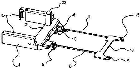
The gripping arm illustrated in Figure 7 comprises means for
gripping a plurality of semiconductor wafers 2 by their peripheral part
and means for orientating the gripped semiconductor wafers, which
means co-operate with the gripping means in order to align the respective
positioning marks of the semiconductor wafers gripped by the arm. The
gripping means comprise a plurality of partial structures 7, which are
capable of being respectively inserted into the free spaces between
semiconductor wafers of a support (not illustrated), and they are
connected by a common rigid support 30, as illustrated. Each structure
carries a driving roller for rotating the wafer which this structure is
intended to support, three stops 8 for supporting this wafer, and two
beams 21 and 24, as described previously for a structure 7. The arm
illustrated in Figure 7 makes it possible to grip, advantageously
simultaneously, a plurality of wafers ? placed in a support and to
orientate, advantageously simultaneously, these wafers so as to place
them in a defined position, for example so as t:o align their notches 3.
CA 02331079 2000-10-30
22
Thus the notches may be aligned, for example, while the wafers are being
transferred from one place to another.
Several examples of the methods according to the invention will
now be described. A first example of the method according to the
invention comprises a mechanical method permitting a change in
position of one or more semiconductor wafers provided with a notch and
placed in a support intended to house a plurality of semiconductor
W afers, consisting in gripping the semiconductor wafer or wafers by its
or their peripheral part and orientating the semiconductor wafer or wafers
in order to place its or their notch (or notches) in a defined position.
Such a method may, for example, be implemented by a device according
to the invention, as described above, permitting, more especially, an
alignment of the notches of the semiconductor wafers placed in a support
without removing these wafers from their support.
A second example of the method according to the invention consists
in moving the semiconductor wafer or wafers from one place to another
and simultaneously orientating it or them so as to place its or their notch
(or notches) in a defined position, for example so as to align the notches.
Such a method may, for example, be implemented by a device for
transferring wafers, as described above.
CA 02331079 2000-10-30