Note: Descriptions are shown in the official language in which they were submitted.
CA 02331194 2001-O1-17
Capasso 59-97-12-24-28-9
DISTRIBUTED FEEDBACK SURFACE PLASMON LASER
Background Of The Invention
The present invention relates to a surface plasmon laser structure and, more
particularly, to a surface plasmon laser including a distributed feedback
(DFB) structure
to provide long wavelength, single mode operation.
Summary Of The Prior Art
Existing technologies for long wavelength injection lasers based on interband
transitions in III-V semiconductor materials are typically limited to 7~< 5
pm, leaving a
considerable part of the mid- to far-infrared spectrum accessible only by lead-
salt lasers.
However, quantum cascade (QC) lasers operatin~,~ on intersubband transitions
between
conduction band states in InGaAs/AIInAs heterostructures have proven so far to
be
extremely versatile, covering the range of wavelengths of the two atmospheric
windows
(3.4 - 13 ~tm), and providing high optical power at room temperature. When
formed as
a distributed feedback (DFB) device (including a grating structure embedded in
the
I5 optical waveguide in the immediate vicinity of the active region), single
mode operation
is possible. Optical waveguiding is achieved by virtue of the inner core
(active) region
having a higher refractive index than the surrounding (outer) cladding region.
At longer
wavelengths, however, the total thickness of the waveguide layers (core plus
claddings)
becomes difficult to handle and, moreover, light absorption by free carriers
(particularly
in the relatively high doped n-type QC cladding layers) results in even
greater signal
losses. Additionally, DFB structures operating at longer wavelengths require
an
extremely deep etch to form the grating structure, making regrowth problematic
and
leaving weakly coupled gratings far away from the active region as the only
option. All
of these difficulties result in the DFB structure being an unattractive
candidate for long
wavelength applications.
However, Maxwell's laws of electromagnetism allow for another type of optical
confinement to take place at the interface between two different homogeneous
materials. These light waves exist, characterized by an exponentially decaying
intensity
in the two directions normal to the interface, provided the dielectric
constants (E) of the
CA 02331194 2001-O1-17
Capasso 59-97-12-24-28-9 2
two materials have real parts of opposite sign. For a given radiation
frequency, one
single confined mode results, with the magnetic field polarized parallel to
the interface
and normal to the propagation direction (i.e., transverse magnetic (TM)
polarization).
Dielectric constants having a negative real part typically appear in the
electromagnetic response of charged harmonic oscillators, more specifically,
at
frequencies above the oscillator resonance coo and up to a frequency c~L,
where E(c~L)=0
and purely longitudinal modes can propagate. In metals or high-doped
semiconductors,
the existing nearly free electrons behave as simple oscillators of exactly
zero resonance
frequency for transverse excitation, while at the same time displaying very
high wL,
generally in the visible or even in the UV wavelength range. The latter takes
the name
of "plasma frequency" c~P, being the frequency of charge density oscillations.
Thus,
metals present an extremely wide range of wavelengths where Re[sJ < 0, and
where the
metals can support the interface-confined electromagnetic waves, the waves
referred to
as "surface plasmons". The possibility of using surface plasmons in place of
more
1 S conventional multi-layer dielectric waveguides at optical frequencies has
been recently
explored in the field of mid-infrared semiconductor lasers. However, the
marginal
performances of these surface plasmon devices cannot compete with those of
traditional
layered structures.
There remains a need in the art, therefore, for a relatively long wavelength
laser
(i.e., ~,>ISpm) that is not prohibitively thick, nor as technically difficult
to manufacture
as DFB devices.
Summary Of The Invention
The need remaining in the art is addressed by the present invention, which
relates to a surface plasmon laser structure and, more particularly, to a
surface plasmon
laser including a distributed feedback (DFB) structure for providing single
mode, long
wavelength (e.g., ~,=17~m) emission.
A surface plasmon laser includes an active region formed as an insulated ridge
structure and further comprises a metal surface layer disposed longitudinally
along the
CA 02331194 2003-07-28
ridge, contiguous with the active region. The structure results in the
formation of
surface plasmon propagation, where at wavelengths greater than 1 ~ prn it has
been
found that the power loss associated with penetration depth (i.e., skin depth)
into the
metal is largely reduced., The resultant large mode confinement I' with the
attendant
reduced thickness of the waveguide layers (reduced from a prior art thickness
of
approximately 9pm to less than 4pm) is advantageously used to create a long
wavelength laser.
In accordance with the teachings of the present invention, the metal surface
layer comprises a metallic grating, (i.e., periodic) surface structure, thus
forming a DFB
surface plasmon laser capable of single mode emission. In one embodiment,
titanium
stripes are first deposited on the c~xloosed surface of the active region,
followed by a
continuous layer of gold. 'the resulting 'ri/Au~-Au grating provides single
mode
plasmon radiation output, where the output wavelength can be "tuned" by
modifying
the operating temperature of the device.
1 _'i In a particular embodiment of the present invention, the active region
of the
DFB surface plasmon laser may comprise a quantum cascade (QC.') structure,
including
a multiplicity of essentially identical repeat units, each repeat unit
comprising one or
more quantum wells. Successive carrier transitions from a higher to a lower
energy
state result in photon emissions, with the photc»~ energy depending on the
structurf; and
compositional details of the repeat unit.
In accordance with one aspect of the present invention there is provided an
article comprising a surface plasmon laser strueaure comprising: a
semiconducting
substrate having a top major surface; an active region disposed to cover a
portion of
said semiconducting substrate top major surface, said active region formed as
a ridge
2'_~ including sidewalk and a top surface; a metallic surface plasmon carrying
layer
disposed to cover a portion of said active region top surface; an insulating
layer
disposed to cover said active region sidewalk and exposed regions of said
semiconducting substrate top m~rjor surface; and electrical contacts coupled
to a bottom
major surface of said serniconductirtg substrate to facilitate flowing an
electrical current
CA 02331194 2003-07-28
3a
through the laser characterized in that the surface plasmon laser comprises a
single
mode device and the metallic surface plasmon carrying layer comprises: a
multiple
layer metallic arrangement formed as a distrib~~tecl feedback (DF'B) grating
arrangement
exhibiting a periodic Bragg structure.
Other and further advantages and arrangements of the present invention will
become apparent during; the courae ofthe following discussion and by reference
to the
accompanying drawings.
Brief Description Of The Drawings
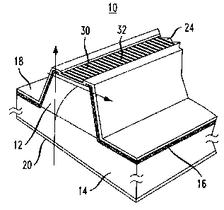
FIG. 1 is an isometric view of a DFB plasmon laser formed in accordance with
the present invention;
FIG. 2 is an illustration of the front facet of the device of FIG. l;
CA 02331194 2001-O1-17
Capasso 59-97-12-24-28-9 4
FIG. 3 is a cut-away side view of the single mode DFB surface plasmon laser of
FIG. I ;
FIG. 4 is a graph comparing the mode intensity and the real part of the
dielectric constant of an exemplary surface plasmon laser formed in accordance
with the
present invention with a conventional dielectric waveguide;
FIG. 5 is a graph illustrating the L-I characteristics and current-voltage
characteristic of an exemplary surface plasmon laser;
FIG. 6 illustrates the single mode output from an exemplary DFB surface
plasmon laser of the present invention;
FIG. 7 illustrates an exemplary conduction band diagram of the active region
for
an exemplary DFB quantum cascade (QC) surface plasmon laser of the present
invention;
FIG. 8 depicts the ability to "tune" the output wavelength of a single mode
DFB-QC plasmon laser of the present invention, tuning as a function of laser
ambient
1 S temperature;
FIG. 9 illustrates one exemplary utilization of the DFB surface plasmon laser
of
the present invention, in this case as part of a point sensing apparatus; and
FIG. 10 illustrates an exemplary remote-sensing system including a DFB surface
plasmon laser as part of the gas-sensing arrangement.
Detailed Description
Mid- to far-infrared semiconductor lasers are typically employed in gas
sensing
applications, where spectroscopic techniques with high resolution and
sensitivity should
be implemented. For this purpose, therefore, single mode devices are desired.
In most
cases, QC laser or diode lasers implementing a DFB resonator (incorporating a
grating
of appropriate period and strength) are used as the single mode device. Such a
structure
introduces a modulation of the refractive index neff and of the attenuation
coefficient oc".
CA 02331194 2001-O1-17
Capasso 59-97-12-24-28-9 5
(or of the effective net gain) favoring the optical mode which best matches
the grating
period over all other possible longitudinal modes.
An isometric view of an exemplary single mode surface plasmon laser 10
formed in accordance with the present invention is illustrated in FIG. 1.
Laser 10
includes an active region 12 formed of, for example, InGaAs/AIInAs, grown on
an InP
substrate 14. Active region 12 is formed as a ridge (using wet chemical
etching, for
example), with an insulator 16 deposited on the sides of the ridge, as well as
across the
top surface of InP substrate 14. Silicon dioxide is an exemplary insulator
useful for this
purpose. A front facet view of laser 10 is shown in FIG. 2 and clearly
illustrates the
location of insulator 16 on the side surfaces of active region 12 and top
surface of
substrate 14. Top electrical contact 18 and bottom electrical contact 20 are
then formed
(using e-beam evaporation, for example), leaving a wide portion of top surface
22 of
active region ridge 12 exposed for the following deposition of a metallic
surface
plasmon carrying layer 24.
In accordance with the present invention, the surface plasmon nature of the
electromagnetic mode advantageously provides for incorporating a DFB structure
in the
laser without the necessity of using any etching procedures. The particular
metals
chosen for the surface metallic layer of the surface plasmon structure have
been found
to strongly affect the penetration depth of the mode, and with it both the
refractive index
and attenuation loss factor. In one embodiment, metallic layer 24 may comprise
a layer
of gold (approximately 300nm thick, for example), which provides for a
relatively large
negative value for the real part of the dielectric constant (Re [gyp"] ~ -1.1
x 104 at ~, ~ 17
p,m) and a relatively shallow penetration depth into the metal. Alternatively,
titanium
(which exhibits a much less negative dielectric constant - Re [sT;] ~ -1x10³
at ~, = l7pm
- and larger penetration depth) may be used. For example, deposition of a
relatively
thin (e.g., I Onm) of titanium before a thicker (e.g., 300nm) layer of gold
yields a
variation of the refractive index Onet~/nzt~-~ 1.8x10⁻³ and a variation of the
attenuation
losses ~a.,~/ocW ~ 1.5x10-z with respect to pure gold. By introducing spatial
modulation
into this variation across the ridge of an exemplary surface plasmon laser of
the present
invention, a single mode, long wavelength DFB device may be formed. One
exemplary
CA 02331194 2001-O1-17
Capasso 59-97-12-24-28-9 6
embodiment, as illustrated in FIGS. I-3, includes a dual-metallic Ti/Au-Au
structure. In
particular, optical contact lithography (or any other suitable process) may be
used to
form a first-order Bragg grating (exhibiting a nominal duty cycle of 50%) of
titanium
stripes 30, as shown in FIG. 3, where a deposition of l Onm of titanium has
been used.
A subsequent evaporation of a relatively thick (e.g., 300nm) gold layer 32
effectively
results in an alternate sequence of Ti/Au and pure Au stripes 30,32 across top
surface 22
of active region 12, as illustrated in FIG. 3. Although this particular
embodiment uses a
dual metal structure, various other multiple metal grating structures can be
used. For
example, a tri-metal grating structure may be used.
The relationship Re[s] = r7' - k' between the dielectric constant s, the
refractive
index r~, and the extinction coefficient k implies that materials with
negative Re[c] are
usually very absorptive. For this reason, the attenuation coefficient a. of a
surface
plasmon guided mode depends strongly on the penetration (or skin) depth S in
the
metallic carrying layer (layer 24 in device 10 of FIGS. 1 and 2), decreasing
as the latter
is decreased. With E, being the dielectric constant of the metal (layer 24)
and c2 being
the dielectric constant of the semiconductor (active region 12), penetration
depth 8 can
be expressed as follows:
8 = 1 Re ~y _ 1
2 c s1 + s2
_,
S - 1 Re try 1 -1
2 c ~~ + s2
where ~/2~ is the frequency of the electromagnetic wave and c is the speed of
light in
vacuum. From the above, it follows that a large negative Re[~,] (k2»n2)
implies a
small 8, which entails a lower optical loss. From the above, the attenuation
a, can be
easily derived in the case of a real positive EZ:
CA 02331194 2001-O1-17
Capasso 59-97-12-24-28-9 7
~'~2 Im[~~ ~
3mz
~e[~~ ~~~z + Re[E, ~~
E~ ~ Im ~ E, ~ ro
= l 3 1/2 C
~Re~s,~(Ez+Re~E,~ )~
To a first approximation, the frequency-dependent dielectric constant of a
metal can be
represented by the simple Drude free-carrier expression:
Re[s, (co)] = Ed 1 _ roe, ,
r~ - + y
,
Re[s, ~r~~] = s'~ 1- .,
r~-+y_
,
s
~~~ +Y-~
where s« is the background dielectric constant and y' is a phenomenological
scattering
time.
It has been discovered in accordance with the present invention that surface
plasmon waveguides become less lossy as the radiation wavelength is increased,
owing
to the Lorentzian dependence of E. Metallic waveguides are, in fact, commonly
used in
microwave applications and, although they present more complicated three-
dimensional
geometries allowing also for TE and TEM mode propagation, in the simplest
designs
(i.e., "microstrips"), the fundamental TM mode is again of a surface plasmon
nature.
FIG. 4 shows the dielectric profiles with the corresponding surface plasmon
mode calculated using the transfer matrix method, together with the values of
the
confinement factor r (defined as the normalized integral of the optical mode
over the
active material), waveguide attenuation oc",, and modal effective refractive
index nets-.
For comparison, the mode profile associated with a conventional prior art
CA 02331194 2001-O1-17
Capasso 59-97-12-24-28-9 8
semiconductor-cladding waveguide is also shown. As evident from the graph of
FIG. 4,
the thickness of the epitaxial growth is reduced from the prior art value of
almost 9pm
to less than 4pm, while at the same time concentrating the field intensity in
the active
material, thereby raising T from 0.47 to 0.81.
S The light output (L) - current (I) (solid lines) and current-voltage (V)
(dashed
line) characteristics of a 1.4 mm long and 34 um wide, deep etched, ridge
waveguide
laser operated in pulsed mode (SO ns pulse width, 5 kHz duty-cycle) is shown
in FIG. S.
The optical power is measured from a single facet with ~SO% collection
efficiency. The
I-V characteristic is measured at a temperature of SK, where the L-I curves
are shown at
temperatures indicated in the graph.
FIG. G illustrates the output of an exemplary DFB surface plasmon laser of the
present invention. AS sh0\~'Il, the single mode, pulsed emission is clearly
evident at a
wavelength of 16.2um, with the side modes suppressed well below the 10-~
level.
In one particular embodiment of the present invention, active region 12 of the
1 S device may comprise a quantum cascade (QC) structure. In general, a
quantum cascade
structure consists of a large number of superlattice/injector states, grown
for example by
solid-source MBE in the InGaAs/AIInAs material system, and lattice-matched to
the
InP substrate. FIG. 7 illustrates an exemplary conduction band diagram for an
exemplary QC superlattice/injector structure. In particular, the energy
potential
difference within the QC active material variable period superlattices is
obtained by
periodically alternating nanometer-thick layers of two different
semiconductors, to split
the conduction band (superlattice region) in narrower energy bands
("minibands")
separated by energy gaps ("minigaps"). Laser action can be achieved between
the states
at the edge of the first minigap through unipolar electron injection via
miniband
2S transport. According to the action of QC devices, multiple superlattice
regions are
bridged together by specially designed injectors which, under the appropriate
bias
conditions, extract electrons from the lower miniband of one superlattice to
inject them
into the second miniband of the following one. In this way, many photons can
be
emitted by each single electron traversing the superlattice region/carrier
injector region,
leading to large differential quantum efficiencies (usually much larger than
unity).
CA 02331194 2001-O1-17
Capasso 59-97-12-24-28-9 9
Advantageously, the intersubband and interminiband transitions in
semiconductor
heterostructures are particularly well-suited for surface plasmon waveguides,
due to the
intrinsic TM polarization resulting from their selection rules.
The particular diagram as shown in FIG. 7 illustrates a band structure under
an
applied bias of 20.SkV/cm. The actual layer thicknesses in nanometers for an
active
region/injector stage are (from left to right, starting from the first
barrier):
1.5/6.4/0.6/7.2/0.7/8.3/0.7/9.0/0.6/9.6/2. S/4. 7/2. 0%.2/1. 7/5. 2/1. 515.2.
The Alo.4gIno_SZAs
layers (energy barriers) are in bold symbols, alternated with the
Gao_4~Ino.s3As wells.
The underlined layers are doped to nz = 2.5 x 101' cm 3; italic style
indicates the injector
region. The moduli squared of the relevant wavefunctions in the active and
injector
regions are shown, as is the laser transition (indicated by the wavy arrows in
the active
regions).
,As mentioned above, it is possible to "tune" the laser frequency of a DFB
surface plasmon laser by modifying the ambient temperature of the device,
thereby
changing its effective refractive index. FIG. 8 includes a plot of a tuning
curve of an
exemplary DFB surface plasmon laser (and including in an insert the spectra
recorded at
the various wavelengths). For the example illustrated in FIG. 8, a single mode
laser that
was 23 pm wide and 1.5 mm long was used, the laser having a Ti/Au - Au
periodic
grating structure with a period of 2 pm. As shown, the temperature was varied
over the
range of 5 - 120 K and produced a wavelength variation from approximately
16.18 ~m
to almost 16.26 Vim. Although the illustrated dependence is evidently non-
linear, a
linear tuning coefficient can be defined at the highest temperatures. For the
particular
results illustrated in FIG. 8, a tuning coefficient having a value of 1 nm/K
is an
acceptable approximation.
It is to be understood that the above-described DFB surface plasmon laser
structures are merely illustrative of the many possible specific embodiments
which can
be devised to represent applications of the principles of the present
invention.
Numerous and varied other arrangements can be devised in accordance with these
principles by those skilled in the art without departing from the spirit and
scope of the
invention. In general, there exist many diverse applications for such a single
mode,
CA 02331194 2001-O1-17
Capasso 59-97-12-24-28-9 10
long wavelength device. A first application is illustrated in FIG. 9, which
schematically
depicts a point sensing apparatus including a DFB surface plasmon laser 40 of
the
present invention. Typically, the laser is mounted on a temperature-controlled
stage
(not shown) for coarse wavelength tuning. Mid-IR radiation 42 from DFB surface
plasmon laser 40 passes through a conventional gas cell 44 (optionally a multi-
pass
cell), with exited radiation 46 impinging on a conventional detector 48. The
electrical
output from detector 48 is supplied to a lock-in amplifier 50 (together with
an
appropriate modulation signal, e.g., a l.2kHz sine wave from a modulation
signal
generator 52), and the output from lock-in amplifier 50 is supplied to a
computer 54 for
data analysis and formatting. The data is then displayed and/or stored in any
suitable
manner, such as on a visual display 60. DFB surface plasmon laser 40 is pumped
with
an appropriate electric current. For example, a low frequency current ramp
(e.vT., 250
ms period) from a ramp current generator 56, short bias pulses (e.g., 5 ns
pulse width, 2
~s period) from a bias current generator SS, and a modulation signal from
modulation
current generator 52 are supplied to a combiner 62, and the resultant current
ramp with
superimposed current pulses and sine wave is applied as the pulse input to DFB
surface
plasmon laser 40. The current ramp serves to sweep the laser temperature over
a
predetermined range, and the pulses cause the emission of short laser pulses.
The pulse
wavelength is slowly swept over a range of wavelengths, and absorption as a
function
of wavelength is determined. Thus, the presence in the cell of a gas that has
an
absorption line in the range of wavelengths is readily detected, and the gas
can be
identified. As those skilled in the art will recognize, some conventional
features are not
shown in FIG. 9. For instance, the measurement set-up will typically be under
computer control, requiring further inputs to, and outputs from, computer 54.
Further,
various other arrangements may be used to drive the laser and tune the
temperature/wavelength. The arrangement as depicted in FIG. 9 is considered to
be
exemplary only and not to limit the scope of the teachings of the present
invention.
FIG. 10 schematically depicts an exemplary remote sensing system 60, wherein
emission source 62 (e.g., a factory) emits gaseous emission cloud 64. A DFB
surface
plasmon laser 66 in accordance with the present invention emits radiation 68
which
propagates through emission cloud 64 and is reflected (such as by means of a
corner
CA 02331194 2001-O1-17
Capasso 59-97-12-24-28-9 11
reflector 67). Reflected radiation 69 is then detected by a detector 70. DFB
surface
plasmon laser 66 can be pumped in any appropriate manner (such as described
above in
association with FIG. 9, for example) and the output from detector 70 can be
utilized in
any appropriate manner (also as described above). A mirror or other
appropriate
reflector can be used in place of corner reflector 67. The reflector may be on
an aircraft
or any elevated feature, including the smoke stack that is being monitored. Of
course,
the detector could also be on an aircraft, or be on an elevated feature. In
general, any
arrangement that results in a line-of sight disposition of laser and detector
is
contemplated.
The DFB surface plasmon laser of the present invention will generally be
mounted in an appropriate housing for protection and control. The package will
typically comprise cooling means (e.g., water cooling or thermoelectric
cooling),
temperature sensor means (e.g., a thermocouple) for use in a feedback loop for
temperature control, and means for applying the pump current to the laser. The
laser is
attached in conventional fashion to the cooling means. Optionally, the housing
may
also contain detector means for controlling laser output power. The housing
will
typically have a window that is transparent for the laser radiation, and will
typically be
evacuated or filled with inert gas.