Note: Descriptions are shown in the official language in which they were submitted.
CA 02331424 2000-11-07
WO 991607$7 PCTIUS99I11093
NIGHT 'CIE WF:R
AND LASER RANGE FINDER
BACKGROUND OF THE I:~tVENTION
FIELD OF THE INVENTION
The present invention is in the field of night vision devices of the Iight
amplification type. More particularly, the present: invention relates to an
improved
night vision device having an image intensifier tube (I2T). Also, the present
invention
is in the field of laser range finders. A method o~F operating the night
vision device
and a method of laser range finding (LRF) are disclosed also.
Related Technolony
Laser range finders have been known for a considerable time. These devices
are used, for example, by surveyors to calculate the distance from a point of
observation to an object such as a geological forniation in the field of view
(i.e., the
device requires line of sight relationship between a user and the object to be
ranged).
Generally, a laser range finder operates by projecting a pulse of laser light
at an object.
The laser light illuminates the object, and a portion of the laser light is
reflected back
toward the laser range finder device. The reflected laser light is detected,
and the time
interval required for the laser light pulse to travel tto and from the object
is measured.
Frorn this time interval measurement and the known speed of light, the
distance
between the laser range finder and the object is calculated.
A conventional laser range finder of the type described above generally
includes a Iaser capable of producing laser light pulses of high peak power
and very
short duration (i.e., less than SOns duration). The detector for the reflected
laser light
may include a high speed photodetector (such as an InGaAs avalanche
photodiode),
which is coupled to a high gain, high speed amplifier. A high speed digital
counter
1
CA 02331424 2000-11-07
WO 99160787 PCT/US99111093
may be used as a timer to determine the time interval required for the laser
Light to
travel to the object and for laser light reflecting off' of the object to
travel back to the
device. From this time interval information an internal electronic calculator
determines the range to the object, and this range is presented to the user of
the
device, usually on a visual display screen.
These conventional laser range finders have a disadvantage of a considerable
cost and complexity. The laser pulses must be of considerable intensity as
well,
which requires a high power laser. The conventional laser range finders are
subject to
optical and electrical problems, such as vuinerabil:ity to electromagnetic
interference,
damage to electrical components and damage to optical components. Reliability
of
the devices is also adversely impacted by their complexity.
~n the other hand, conventional night vision devices of the image
intensification type (i.e., light amplification) type have also been known for
a
considerable time. Generally, these night vision devices include an objective
lens
which focuses invisible infrared Light from the night time scene onto the
transparent
light-receiving face of an image intensifier tube. At its opposite image-face,
the
image intensifier tube provides an image in visible yellow-green
phosphorescent light,
which is then presented to a user of the device via an eye piece lens.
Even on a night which is too dark for diurnal vision, invisible infrared Light
is
richly provided by the stars. Human vision can not utilize this infrared Light
from the
stars because the so-called near-infrared portion. of the spectrum is
invisible for
humans. A night vision device of the light amplification type can provide a
visible
image replicating the night time scene.
A contemporary night vision device will generally use an image intensifier
tube with a photocathode behind the light-receiving face of the tube. The
photocathode is responsive to photons of infrared light to liberate
photoelectrons.
These photoelectrons are moved by a prevailing electrostatic field to a
microchannel
plate (MCP) having a great multitude of dynodes, or microchannels with an
interior
surface substantially defined by a material having a high coefficient of
secondary
electron emissivity. The photoelectrons entering the microchannels cause a
cascade of
2
CA 02331424 2000-11-07
WO 99!60787 PCT/US99/11093
secondary emission electrons to move along the mic;rochannels so that a
spatial output
pattern of electrons which replicates an input pattern, and at a considerably
higher
electron density than the input pattern results. This pattern of electrons is
moved from
the microchannel plate to a phosphorescent screen to produce a visible image.
A
power supply for the image intensifier tube provides the electrostatic field
potentials
referred to above, and also provides a faeld and current flow to the
microchannel plate.
Conventional night vision devices which .are usable to sight a weapon are
found in United States patents No. 5,084,780; and 5,035,472. Neither of these
patents
is believed to suggest or disclose a night vision device which is combined
with a laser
range finder using the image intensifier tube of thE: night vision device as a
detector
for laser light in the laser range finder.
SUMMARY OF THE INVENTION
In view of the deficiencies of the conventional related technology, it would
be
desirable to provide a single device which provides both night vision imaging
and
Iaser range finding functions.
Additionally, it would be desirable to provide a laser range finder which uses
an image intensifier tube as a detector for reflected laser light from an
object.
Yet another advantage would be to providf; such a device which allows both
night-time and day-time imaging and laser range Finding using the image
intensifier
tube of the imaging device as the detector for reflected laser light.
Still another advantage could be obtained b;y provision of such a device which
utilizes the image intensif er tube as a detector for reflected laser light in
the LRF
function, and which also includes electrical amplification of the electrical
signal
produced when this laser light is detected, therefore to provide an improved
signal to
noise ratio for the LRF function.
Accordingly it is an object for this invention to provide a method of laser
range finding using an image intensifier tube as a detector for reflected
laser light, and
in which the image intensifier tube includes provision internally for
amplifying an
3
CA 02331424 2000-11-07
WO 99160787 PCTIUS99/11093
electrical signal indicative of the detection of reflected laser light during
a LRF
function.
An advantage of the present combined night vision device and laser range
finder is that a single device is provided of considerably less expense and of
considerably improved durability in comparison to the conventional technology
providing these functions in two separate devices. The laser pulses needed for
laser
range finding can be of remarkably lower power than those required by a
conventional
laser range finder. This further decreases the cost of the device because of
the lower
cost of a lower power Laser, and the energy use of the device is also
decreased.
Other obj ects, features, and advantages ~of the present invention will be
apparent to those skilled in the art from a consideration of the following
detailed
description of a preferred exemplary embodiment thereof taken in conjunction
with
the associated figures which will first be described ibriefly.
BRIEF DESCRIPTItJN OF THE DRAWINGS
Figure 1 is a schematic representation of an integrated night vision device
and
laser range finder embodying the present invention, and with a part of this
device
shown in alternative operative positions by use of solid and dashed lines;
Figure 2 shows an image intensifier tube embodying the present invention in
longitudinal cross section;
Figure 3 is a schematic representation of a power supply and laser range
finder
operation circuit for an integrated night vision device and laser range finder
embodying the present invention;
Figure 3a is a fragmentary schematic representation of an alternative
embodiment of an image intensifier tube module for use in an integrated night
vision
device and Laser range finder according to the present invention; and
Figures 4 and 5 respectively provide graphical illustrations of an automatic
brightness control (ABC) function, and of a bright-source protection (BSP)
function
of the integrated night vision device and laser r~uige finder embodying the
present
invention.
4
CA 02331424 2000-11-07
WO 99/60787 PCT/US99/11093
DETAILED DESCRIPTION OF AN EXEMPLAvRY
PREFERRED EMBODIMENT OF THE INVENTI N
While the present invention may be embodied in many different forms,
disclosed herein is a specific exemplary embodiment that illustrates and
explains the
principles of the invention. It should be emphasized that the present
invention is not
limited to the specific embodiment illustrated.
NIGHT VISION
Refernng first to Fig. l, there is shown schematically the basic elements of
one
version of an integrated night vision device and laser range finder 10.
Particulars of
the laser range finding (LRF) operation of the device are presented below. In
order to
provide night vision, the device 1d generally comprises a forward objective
optical
lens assembly 12 (illustrated schematically as a single lens, although those
ordinarily
skilled will understand that the objective lens assembly 12 may include plural
lens
elements). This objective lens 12 performs at least two functions in the
device 10,
lens I2 focuses incoming light from a distant scene through the front light-
receiving
end 14a of an image intensifier tube 14 (as will bE; seen, this surface is
defined by a
transparent window portion of the tube - to be further described below). As
was
generally explained above in the discussion of the related technology, the
image
intensifier tube 14 provides an image at light output end 14b in
phosphorescent .
yellow-green visible light. This image replicates th,e scene being viewed by
use of the
device 10.
The scene being viewed by use of device 10 may be a dark night-time scene
which is invisible, or is only poorly visible, to the user of the device 10
using natural
human vision. On the other hand, as will be explained, the device 10 may be
used to
view a day-time scene, and to conduct laser range finding (LRF) in both
daylight and
at night. The visible image from tube 14 is presented by an eye piece lens
illustrated
schematically as a single lens 16 producing at the user's eye a virtual image
of the rear
light-output end 14b of the tube l 4.
5
CA 02331424 2000-11-07
WO 99/60787 PCT/US99/11093
More particularly, image intensifier tube 14 includes a photocathode 20 which
is responsive to photons of light at the deep red endl of the visible spectrum
and in the
near-infrared portion of the spectrum to liberate photoelectrons in a pattern
replicating
the scene being viewed, a microchannel plate (MCP) 22 which receives the
photoelectrons in the pattern replicating the scene, and which provides a
greatly
amplified pattern of electrons also replicating this scene, and a display
electrode
assembly 24 having an aluminized phosphor co<~ting or phosphor screen 26. A
transparent window portion 24a of the assembly 24 carries the electrode 24 and
screen
26, and also conveys the image from screen 26 outwardly of the tube 14 so that
it can
be presented to the user 18. Window portion 24a defines surface 14b.
Still more particularly, MCP 22 is located ,just behind photocathode 20, with
the MCP 22 having an electron-receiving face 28 and an opposite electron-
discharge
face 30. This MCP 22 further contains a plurality of angulated microchannels
32
which open on an electron-receiving face 28 and on an opposite electron-
discharge
face 30. Microchannels 32 are separated by passage walls 34. At least a
portion of
the surfaces of the walls 34 bounding the microchannels 32 is formed by a
material
having a high coefficient of emissivity of secondary electrons. Thus, the
channels 32
of the MCP 22 are each a dynode, emitting a shower of secondary electrons in
response to receipt at face 28 of photoelectrons from photocathode 20.
The display electrode assembly 24, generally has a coated phosphor screen 26,
and is located behind MCP 22 with phosphor screen 26 in electron line-of sight
communication with the electron-discharge face 3(). This display electrode
assembly
24 is typically formed of an aluminized phosphor screen 26 deposited on the
vacuum-
exposed surface of the optically transparent material of window portion 24a.
The eye
piece lens 16 is located behind the display electrode assembly 24 and allows
an
observer 18 to view a correctly oriented image corresponding to the low level
image
(i.e., dim or invisible, perhaps) of the scene being viewed.
As will be generally appreciated by those skilled in the art (now also viewing
Figure 2), the individual components of image intensifier tube 14 are all
mounted and
supported in a tube or chamber (to be further explained below) having forward
and
6
CA 02331424 2000-11-07
WO 99/60787 PCTNS99/11093
rear transparent plates cooperating to define a chamber (to be fuxther defined
below)
which has been evacuated to a low pressure. 'This evacuation allows electrons
liberated into the free space within the tube (i.e., i;he photoelectrons and
secondary-
emission electrons) to be transferred by prevailing electrostatic fields
between the
various components without atmospheric interference that could possibly
decrease the
signal-to-noise ratio.
As indicated above, photocathode 20 is mounted immediately behind objective
lens 12 on the inner vacuum exposed surface of th.e window portion of the tube
and
before MCP 22. It is upon this photocathode treat the objective lens 12
actually
focuses the image of the distant scene, through tl~e window portion which
defines
surface 14a. Typically, this photocathode 20 i.s a circular disk-like
structure having a
predetermined construction of semiconductor materials, and is mounted on a
substrate
in a well known manner. Suitable photocatho~de materials are generally semi-
conductors such as gallium arsenide; or alkali meW 1s, such as compounds of
sodium,
potassium, cesium, and antimony (commercially available as S-20). The
photocathode is carried on a readily available substrate which is transparent
to light in
the wavelength band of interest (i.e., ordinarily i.n the deep-red and near
infrared
portion of the spectrum; extending in some cases to the blue portion of the
visible
spectrum - but which is not necessarily transparent to all visible light). A
variety of
glass and fiber optic substrate materials are commercially available.
Still referring to Figure 2, and considering in somewhat greater detail the
operation of the image intensif er tube 14 in its mode of operation providing
a visible
image it is seen that in response to photons 36 entering the forward end of
night vision
device 10 and passing thraugh objective lens 12, photocathode 20 has an active
surface 38 from which are emitted photoelectrons in numbers proportionate to
and at
locations replicative of the received light from the scene being viewed. In
general, at
night the image received by the device 10 will be too dim to be viewed with
human
natural vision, and may be entirely or partially of infrared radiation which
is invisible
to the human eye. The device may also operate in daylight to provide an image,
as
will be explained. It is thus to be understood 'that the shower of
photoelectrons
7
CA 02331424 2000-11-07
WO 99/60787 PCTIUS99I11093
emitted from the photocathode are representative of the image entering the
forward
end of image intensifier tube 14. The path of a typiical photoelectron emitted
from the
photon input point on the photocathode 20 is represented in Fig: 1 by dashed
line 40.
Photoelectrons 40 emitted from photocathode 20 gain energy by passage
through an applied electrostatic field between the 1>hotocathode 20 and the
input face
28. The applied electric field is of a predetermined intensity gradient and is
established between photocathode 20 and electrc'n-receiving face 28 by a power
source diagrammatically depicted in Figure 1 and indicated by the numeral 42.
Typically, power source 42 will apply an electrostatic field voltage on the
order of 200
l 0 to 800 volts to maintain an electrostatic field of the desired intensity.
This field is
most negative at photocathode 20 and most positive at the face 28 of MCP 22.
Further, an electrostatic field most negative at photocathode 20 and most
positive at
output electrode 24 is maintained in the image intensifier tube 14, as will be
seen.
After accelerating over a distance between the photocathode 20 and the input
face 28
of the MCP 22, these photoelectrons 40 enter microchannels 32.
As will be discussed in greater detail below, the photoelectrons 40 are
amplified by emission of secondary electrons in the microchannels 32 to
produce a
proportionately larger number of electrons upon passage through MCP 22. This
amplified shower of secondary-emission electrons 44, also accelerated by a
respective
electrostatic field applied by power source 46, then exits from the
microchannels 32 of
MCP 22 at electron-discharge face 30.
Once in free space again (i.e., in the vacuum environment inside of tube 14),
the amplified shower of photoelectrons and secondary emission electrons is
again
accelerated in an established electrostatic field provided by power source 48.
This
electrostatic field is established between the electtron-discharge face 30 and
display
electrode assembly 24. Typically, the power source 48 produces a field on the
order
of 3,000 to 7,000 volts, and more preferably on the order of 6,000 volts in
order to
impart the desired energy to the multiplied electrons 44.
The shower of photoelectrons and secondary-emission electrons 44 (those
ordinarily skilled in the art will know that considiered statistically, the
shower 44 is
8
CA 02331424 2000-11-07
WO 99!60787 PCT/US99/11093
almost or entirely devoid of photoelectrons and is made up entirely or almost
entirely
of secondary emission electrons. This is the case because the statistical
probability of
a photoelectron avoiding absorption in the microc~hannels 32 is low). However,
the
shower of electrons 44 is several orders of magniaude more intense than the
initial
shower of photoelectrons 40, but is still in a pattern replicating the image
focused on
photocathode 20. This amplified shower of electrons falls on the phosphor
screen 26
of display electrode assembly 24 to produce an irna~;e in visible light.
Viewing Figure 2 in order to acquire a greater understanding of the detail of
a
typical image intensifier tube, the image intensifier tube 14 is seen to
include a tubular
body 50, which is closed at opposite ends by a front Light-receiving window
52, and
by a rear fiber-optic image output window 54. The window 54 defines the light
output surface 14b for the tube 14, and carries t:he coating 26, as will be
fixrther
described. As is illustrated in Figure 2, the rear window 54 may be an image-
inverting type (i.e., with optical fibers bonded together and rotated
180° between the
apposite faces of this window 54 in order to provide an erect image to the
user 18.
The window member 54 is not necessarily of such inverting type. Both of the
windows 52 and 54 are sealingly engaged with the body 50, so that an interior
chamber 56 of the body 50 can be maintained at a vacuum relative to ambient.
The
tubular body 50 is made up of plural conductive metal rings, each indicated
with the
general numeral S8 with an alphabetical suffix added thereto (i.e., 58a, 58b,
58c, and
58d) as is necessary to distinguish the individual rings from one another.
The tubular body sections S8 are spaced apart and are electrically insulated
from one another by interposed insulator rings, each of which is indicated
with the
general numeral 60, again with an alphabetical suffix added thereto (i.e.,
60a, 60b, and
60c). The sections 58 and insulators 60 are sealingly attached to one another.
End
sections 58a and 58d are likewise sealingly attached to the respective windows
52 and
54.
The body sections 58 are individually connected electrically to a power supply
and laser range finder circuit, generally indicated with numeral 62, and best
seen in
Figure 3, (and which includes the power sources diagrammatically illustrated
in
9
CA 02331424 2000-11-07
WO 99/60787 PCT/US99/11093
Figure l and indicated with reference numerals 42" 46, and 48, as described
above).
This circuit 62 is effective during operation of the image intensifier tube 14
to
maintain an electrostatic field most negative at the section 58a and most
positive at the
section 58d. As will be seen, the circuit 62 includes a section indicated with
the
numeral 62a, which is encapsulated with the images intensifier tube 14, and
which is
effective to provide the voltages necessary for operation of this tube. The
image tube
14 and circuit section 62a will be recognized by those ordinarily skilled in
the
pertinent art as an image tube module. Another section 62b of the circuitry
62, seen
together with section 62a in Figure 3, allows control of the operation of a
laser to
provide pulses of laser light, and to operate the image intensifier tube 14 as
a detector
for the reflected laser light in order to allow timing of the light pulses,
and calculation
of the range to a object illuminated by the laser light: pulses.
Further viewing Figure 2, it is seen that the :front window 52 carnes on its
rear
surface within the chamber 56 the photocathode 20. The section 58a is
electrically
continuous with the photocathode by use of a thin metallization (indicated
with
reference numeral 58a') extending between the secrtion 58a and the
photocathode 20.
Thus, the photocathode by this electrical corn<;ction and because of its semi-
conductive nature, has an electrostatic charge distributed across the areas of
this disk-
like photocathode structure. Also, a conductive coating or layer is provided
at each of
the opposite faces 28 and 30 of the MCP 22 (as is indicated by arrowed
numerals 28a
and 30a). Power supply 46 is conductive with these coatings by connection to
housing sections 58b and 58c. Finally, the power supply 48 is conductive with
a
conductive layer or coating (possibly an aluminum :metallization, as mentioned
above)
at the display electrode assembly 24 by use of a nnetallization also extending
across
the vacuum-exposed surfaces of the window member 54, as is indicated by
arrowed
numeral 54a.
Still viewing Figure 2, it is seen that the circuit portion 62a is disposed
within
an encapsulating body 64, which is configured as an annulus extending about
the body
50 of the tube 14. This power supply circuit portion 62a has electrical
connection
with each of the conductive ring sections 58a-d of the tube 14, as is
indicated
CA 02331424 2000-11-07
WO 99160787 PCT/US99/11093
diagrammatically in Figure I. Additionally, as is indicated in Figure 3, this
circuit
portion includes a current transformer 66a and a preamplifier circuit portion
66b both
disposed within the body 64 immediately adjacent to the tube 14.
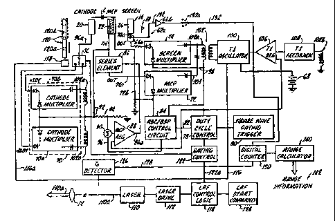
Considering now Figure 3, it is seen that the circuit 62 includes a power
source, which in this case is illustrated as a battery 68. It will be
appreciated that a
battery 68 is generally used as the power source for portable apparatus, such
as night
vision devices. However, the invention is not limilted to any particular power
source.
For example, a regulated line-power source could b~e used to provide input
power to a
power supply implementing and embodying the principles of the present
invention.
Considered generally, the circuit 62 includes three voltage multipliers,
respectively
indicated with the numerals 70, 72, and 74. 'I"he voltage multiplier 70 for
the
photocathode 20 includes two multipliers of differing voltage level, indicated
with the
numerals 70a and 70b. A tri-stable switching :network 76 switches controllably
between alternative conditions either conducting the photocathode 20 to
voltage
I S multiplier 70a, to voltage multiplier 70b, or to are open circuit
position, all via the
conductive connection 76a. In other words, the switching network 76
alternatingly
connects the photocathode 20 of the tube I4 to a voltage source at about -800
volts, or
to a source at about +30 volts relative to the front face of the microchannel
plate, as
will be further seen. The open circuit interval of time employed in the
present
embodiment between connections of the photocathode 20 to the two voltage
sources
70a and 70b is used for purposes of energy efficiency, and is optional. A duty
cycle
control 78 controls the switching position of the switching network 76, and
receives as
inputs a square wave gating trigger signal from an. oscillator 80, and a
control signal
via a conductor 82 from an ABC/BSP control circuit 84. Once again, the use of
a
square wave duty cycle trigger signal is optional. Other forms of duty cycle
trigger
waves can be employed.
Power supply to the MCP 22 (that is, to the conductive layers or
metallizations
28a and 30a) is effected from the voltage multiplier 72 via connections 72a
and 72b.
Interposed in connection 72a is a series element 86, which in effect is a
variable
resistor. A high-voltage MOSFET may be used fc~r element 86, and the
resistance of
Il
CA 02331424 2000-11-07
WO 99/6087 PCT/US99/11093
this element is controlled over a connection 86a by a regulator circuit 88.
Regulator
circuit 88 receives a feed back control signal from a surnrning junction 90,
which
receives an input from conductor 92 via a level-adjusting resistor 94, and
also receives
an input via conductor 96 from the ABCBSP control circuit 84. Conductor 92
also
provides a reference voltage signal of the voltage level applied to the input
face 28
(i.e., at metallization 28a) of the MCP 22 into the voltage multiplier circuit
70.
The voltage multiplier 74 has connection t:o the screen 26 via a connection
74a, and provides a feed back of screen current level into ABCBSP control
circuit via
conductor 98. It will be noted that the conductor 74a passes through the
current
transformer 66a, so that current flow in this conductor 74a is
electromagnetically {i.e.,
inductively) linked to the pre-amplifier 66b. Energy flow in the circuit 62 is
provided
by an oscillator 100 and coupled transformer :102, with output windings 102a
providing energy input to voltage multipliers 70 and 74, and a conductor 104
providing energy to voltage multiplier 72. The oscillator 100 receives a
control feed
back via a regulator 106 and a feed back circuit 108, having an input from a
feedback
winding 102b of transformer 102.
Having generally considered the structure o:f the circuit 62, attention may
now
be given to its operation, and the cooperation of this circuit operation with
the
operation of the image intensifier tube 14 to provide; imaging. It will be
noted that this
imaging of a scene for a user of the device 10 may take place at night in
conditions of
viewing a scene under dark-field conditions, or during the day with the scene
illuminated by sun light. It will be noted also tlhat the voltage level
produced by
voltage multiplier 70a is a substantially constant voltage level. Preferably,
this
voltage is about negative 800 volts. ~n the other hand, the voltage multiplier
section
70b provides a substantially constant voltage level referenced to the voltage
provided
by voltage multiplier 72 to the front face 28a of thf; MCP 22. Preferably,
this voltage
level is positive 30 volts relative to the front face 2!3 of the MCP 22.
By operation of the switching network 76, the photocathode 20 is controllably
and cyclically changed between connection to the constant voltage source 70a,
to an
open circuit (i.e., voltage off), and to the lower voltage provided by source
70b
12
CA 02331424 2000-11-07
WO 99160787 PCTlUS99/11093
(simulating darkness for the photocathode). This gating function is carried on
at a
constant frequency (preferably at about 50 Hz), with a constant cycle
interval, while
varying the duty cycle of the applied constant voltal;e from voltage
multiplier 70a as a
function of current level sensed at screen 26 (i.e., by feed back over
conductor 104).
The frequency of the duty cycle for the photocathade is sufficiently fast
{i.e.,
somewhat above about 30Hz} so that no flicker is perceived in the viewed
image.
Automatic Brightness ControlBright Source Protection
Viewing Figure 4, it is seen that over a first selected range of screen
current
the duty cycle of the applied constant voltage from multiplier 70a to the
photocathode
is fixed at 100%. However, at screen current levels above a selected level of
screen current, the duty cycle progressively ramps down substantially linearly
to a low
level of essentially 10-4% as a function of increasing screen current. For
screen
current levels above that at which the duty cycle for gating of the constant
voltage
15 from source 70a to the photocathode 20 drops to its low level, an
additional function
of BSP is provided by decreasing the voltage applied to the MCP 22. As Figure
5
shows, for all screen current levels lower than those necessary to initiate
this BSP
protection function, the voltage applied across the MCP 22 is a constant. The
reduction of voltage level applied across the MCP :22 for BSP is effected by
action of
20 the series element 86 increasing its resistance under control of MCP
regulator 88.
As noted this regulator 88 receives a .summed input from the voltage
multipliers 70, and from the ABCBSP control circuit 84, which is responsive to
screen current level sensed by conductor 98. An understanding of the voltage
level
experienced as a function of time within duty cycle intervals at the
photocathode 20
can be obtained by noting that a virtual capacitor exists between the
photocathode 20
and the front face 28 of MCP 22. This capacitor exists electrically, but not
as a
conventional capacitor structure. On Figure 3, this virtual capacitor is
diagrammatically indicated, and indicated by the arrowed reference character
"C".
When the duty cycle for the application of the constant voltage supplied by
voltage
multiplier 70a is 100%, or close to this level, then :following the opening of
the circuit
13
CA 02331424 2000-11-07
WO 99/60'78' PCT/US99/11093
through switching network 77, the voltage across the virtual capacitor "C"
decays over
a time interval at a natural open-circuit, capacitor-discharge rate. This
voltage decay
is actually a very small voltage because of the short time interval (i.e.,
1/SOth second
at a SOHz frequency for the gating operation of switching network 76).
Next in each duty cycle, the network 76 conducts the photocathode to voltage
multiplier 70b, which effectively replicates darl~;ness for the photocathode
20 by
dropping the voltage on the photocathode to +30 volts relative to the face 28
of MCP
22. As noted above, this voltage cutoff is provided by having voltage
multiplier 72b
provide a voltage which is about 30 volts positive with respect to the voltage
provided
at coating 28a an the front face of the MCP 22 by voltage multiplier 72.
In essence, when the photocathode 20 operates, it always operates at the high
constant voltage provided by voltage multiplier 70;3. When the photocathode 20
is not
operating, it is switched to a voltage which replicates a dark field for the
photocathode
(i.e., the +30 volts from voltage multiplier 70b). T'he photocathode 20
operated by the
1 S circuit 62 of the present invention is switched between operation at its
designed
voltage level and dark-field condition at a duty cycle which varies dependent
upon the
Light intensity of the scene being viewed, as indicated by current flow at the
screen 26.
This function is carried out in accord with the duty cycle function in order
to provide
ABC. The result of this ABC operation is a substantially constant brightness
for the
image presented to a user of the night vision device 10 is achieved, until the
scene
becomes too dim to produce an image even with image intensification
technology. In
other words, over the entire operating range of the image intensifier tube 14,
its
operation by circuit 62 provides substantially constant brightness for the
image
presented to the user of the device.
Further considering the operation of circuit; 62 to provide an image for the
user
of the device 10, is seen that once the duty cycle is reduced to its low level
of 10-4%,
in the event that screen current increases further, then as a function of
increasing
screen current the voltage across the MCP 22 is reduced slightly, viewing now
Figure
5. This reduction of MCP voltage has the effect of providing BSP. That is,
after the
ABC function has reached its lowest level of duty cycle to the photocathode
20, if
14
CA 02331424 2000-11-07
WO 99160787 PCTlUS99/11093 ..
Light level of the viewed scene continues to increase (indicative of a bright
source in
the scene), then the duty cycle maintains its low 10-4% level, while the
bright-source
protection function explained above is effected.
LASER RANGE FINI?ING
Further considering now Figures 1 and 3, the operation of the device and
circuit 62 to provide a laser range finder function will be explained. The
device 10
further includes a laser I LO capable of projecting; a short-duration laser
light pulse
106a into the scene being viewed by the operator of the night vision and laser
range
finder device I0. This pulse of lasex light is diagrammatically illustrated on
Figure 3
with the arrow 110a. Laser range finding operations are conducted by the
device 10
temporarily using the image intensifier tube 14 as a sensor for the reflected
laser light
returned from the scene being viewed.
Laser 110 is powered by a laser driver circuit, indicated with numeral 112. A
laser range finder (LRF) control logic circuit 114 (the operation of which
will be
further explained below) provides a control input to the driver circuit 112 to
effect
operation of the laser 110, and also provides a control input to the
oscillator 100 via a
conductor 116.
Conductor 116 at a branch 116a thereof also provides a control input to an
actuator 1 I $, which in response to this control input moves a spatial f lter
120 (to be
further described below) first into, and then after' a short interval, out of
the optical
pathway between lens I2 and the image intensifier tube I4, as is indicated by
dashed
lines on Figure 1. The spatial filter 120 is essentially a shutter with a
central aperture,
which blocks returning laser light from portions of the viewed scene other
than in the
central area where the object of interest is located. During a LRF operation,
the
actuator I 18 pauses the spatial filter 120 in the opitical pathway of the
device 10. That
is, there is a controlled momentary pause between the movement of the spatial
filter
into and out of the optical pathway. During the laause of the filter 120 in
the optical
pathway, laser light is projected to an object in t:he viewed field, and
reflected laser
light returned from the object for a LRF operation is received at the device
10.
CA 02331424 2000-11-07
WO 99/6078'1 PCTIUS99/11093
The LRF control Logic circuit 114 also has a control output 122a to a gating
control circuit 122. This circuit has connection to switching network 76, as
is
illustrated. An operator-input command device 1:24 (which may take the form of
a
push button switch, far example) is provided by which the operator of the
device .i0
can indicate a command that a LRF operation be earned out be the device 10.
The
remainder of the elements of the device 10 will be described in connection
with a LRF
operation.
A LASER RANGE FINDTNG OPERATION
Considering Figure 3 still, when the operator of the device 10 wishes to
obtain
range information to an object in the viewed field, the operator centers the
object in
the viewed scene, possibly by using a reticule provided by the device 10, and
makes a
LRF input command at device 124. To repeate, this input command may be
effected
by use of a simple push-button switch, for example. In response to this input
command, the LRF control logic circuit 124 effects the following sequential
activities:
First, the oscillator 100 is shut down by a command over conductor 116. This
command also has the effect of causing actuator 118 to move the spatial filter
120 into
the optical pathway. The shutdown command for the oscillator 100 also is used
to
cause the voltage multiplier 72 to drive the MCP 22 to a high-gain
differential voltage
level. Preferably, this high-gain voltage Level is a. differential voltage of
about i 200
volts across the MCP 22.
Second, the LRF control logic circuit com~:nands the switching netwoxk 76 to
perform a timed switching operation (as is further described below), first
switching
photocathode 20 to the voltage from multiplier 7C)b (i.e., to +30 volts
relative to the
front face of MCP 22 - effecting a hard turn off for the photocathode 20 of
the tube
14); and then later in timed relation connecting this. photocathode to source
70a.
Third, after a time interval of about 3 ms (which is required to allow the
oscillator 80 to stop its operation), the laser light pulse is fired. The
photocathode 20
is then effectively switched to the voltage source of multiplier 70a (i.e., to
about -800
volts). Actually, the photocathode 20 is switched to voltage source 70a in
timed
16
CA 02331424 2000-11-07
WO 99/60787 PCT/US99/11093
relation before the laser light pulse is fired. The: photocathode needs to
settle for
about 200 p.s before the laser is fired. If the device 10 is configured to
project the
laser light pulse from the same lenses used to receive ambient light, then in
order to
provide a non-responsiveness of the device 10 to the back scatter of laser
light which
may occur in the optics of the device the pre-amplifier circuit 62 is caused
to have a
time-dependent gain. One way in which thiis time-dependent gain may be
implemented is to provide a high and time-variant threshold value which the
electron
pulse which will be caused within image intensifier tube 14 by reflected laser
light
must exceed before the signal is provided to stop timer 130. This threshold
value
IO would be high immediately after laser pulse 22 is fired, and would decrease
as a
function of time after the pulse is fired. Another al'''ternative is to have a
step-function
change in the threshold value at a certain time after the laser light pulse is
fired. In
this way, the timer 130 will respond to the electron pulse resulting from
reflection of
laser light from the object of interest in the field of view of the device 10,
rather than
I5 to any back scatter of laser light from surfaces of lenses in the device
10.
Fourth, shortly after the time the LRF cont~~ol logic commands the Laser I 10
to
fire a pulse of laser light into the scene which was being viewed by the user
of the
device 10, this pulse will actually be fired. A time-zero (to) detector I26
detects the
moment of actual firing of this laser light pulse, and provides a signal on
conductor
20 128 which starts the high-speed digital timer 130.. Prior to the moment of
firing of
this laser light pulse, the photocathode is connected to voltage source 70b
(i.e.' to the
+30 volts relative source) for a purpose to be further explained below.
Fifth, when the laser light reflects from an object in the scene, returning
laser
light passes through a central aperture 120a of spatial filter 120, so that
reflections of
25 laser light from other objects in the scene are lblocked (i.e.' having the
effect of
increasing the signal to noise ratio of the returning light pulse).
During day time LRF operations an optical filter 144 may also be used along
with
spatial filter 120 and has the beneficial effect of improving signal-to-noise
level This
is the case because the spectral filter removes some of the background light
from the
30 day-time scene which is present at frequencies close to that of the laser
I10. The
I7
CA 02331424 2000-11-07
WO 99/60787 PCTNS99/11093 _.
operator of the device 10 may select to include optical filter 144 along with
spatial
filter 120 by manipulation of a control 144x
The reflected laser light (still in the form of a pulse) passing to image
intensifier tube 14 causing a pulse of photoelectrons to be released by
photocathode
20, as is graphically depicted on Figure 1 and indicated with the character
"P1". The
pulse Pl of photoelectrons passes to MCP 22, and causes a corresponding pulse
of
secondary-emission electrons "P2" (produced under "high gain" conditions for
the
microchannel plate 22), which electrons pass to the output electrode assembly
24. A
corresponding pulse in the current from screen 26 is detected by amplifier
circuit 66b
because of its inductive relationship with the lead 74a, and the preamplifier
then
provides an amplified output signal. This amplifiied output signal is provided
via a
conductor 132, which preferably is a shielded conductor including a shield
electrode
132a, to provide a timer-stop command to the high.-speed timer 130. Also, if
desired,
another level of amplification (indicated on Figure 3 by numeral 132b and a
dashed
line amplif er symbol) may be interposed in tlhe electrical connection
provided
between the pre-amplif er circuit 66b and the high speed timer 130.
Next, spatial filter 120 is withdrawn from the optical pathway, the oscillator
80 is restarted, and the gating operation of the switching network 76 is
resumed (if it
was operating before the LRF operation as a result of the light conditions in
the field
being viewed. In other words, the explanation below concerning daytime
operations
of the device 10 may be consulted at this time. The image of the scene being
viewed
is thus restored for the user of the device 10. During the LRF operation, the
operator
of the device 10 may detect a flicker in the viewed image along with a very
brief flash
of Iight (i.e., from the pulse of electrons P2 impacting the screen 26). The
LRF
operation takes only about 5ms to complete (although the physical movements of
filter
120 will be somewhat slower than this) so the; user's view of the scene in not
significantly interrupted. The time interval betwE:en the to signal and the
timer-stop
command is provided by the timer 130 to a range calculator 134, which then
supplies
an output (indicated with arrowed numeral 136) of range information to the
object for
the operator of the device 10.
18
CA 02331424 2000-11-07
WO 99/bU787 PCT/US99111093
It will be noted that prior to the firing of the: Laser light pulse, the
photocathode
is connected to voltage source 70b, which is abou~~t +30 volts positive
relative to the
face 28 of microchannel plate 22. This positive voltage level on the
photocathode 20
has the effect of a "hard turn ofd' on the photocalhode, preparing it to be
somewhat
insensitive to photons of laser Light which may be back scattered from
surfaces of the
lenses between laser 110 and the projection outvnardly of the beam 110a. That
is,
laser light may be reflected within the device 10 during the firing of this
laser light
pulse, but the image intensifier tube is momentarily somewhat blinded to this
Light
after the hard turn off effected on photocathode 20, even though voltage
source 70a is
connected before the actual moment of firing of this laser light pulse in
order to
provide charge settling on the photocathode.
DAYTIME IMAGING AND LRF OPERATION
It will be noted that far daytime operation o~f the device 10, the BSP
function is
disabled, and the ABC function of the device 10 allows imaging to be
accomplished
in daylight. Accordingly, the ABC function may be operating the photocathode
at less
than 100% duty cycle. Under these conditions, a LRF operation additionally
momentarily interrupts the duty cycle gating operation carried out by
switching
network 76, and effects the switching of the photocathode 20 to the voltages
provided
by sources 70b and 70a (in sequence as described above) in order to effect the
hard
turn off of the photocathode during laser firing, anal then to allow the
photocathode to
be highly responsive to photons of reflected laser Light in order to provide
the LRF
pulses Pl, as described above.
Figure 3a provides a fragmentary view of an alternative embodiment of the
present invention. In order to obtain reference numerals for use in describing
this
alternative embodiment, features which are the same as, or which are analogous
in
structure or function to, featured depicted and described above are indicated
on Figure
3a using the same numeral used above, and with a prime (') added. Viewing
Figure
3a, it is seen that the image intensifier tube 14' also has a current
transformer 66a and
a pre-amplifier circuit 66b which are also carried on the housing SO' within
the
19
CA 02331424 2000-11-07
WO 99/60787 PCT/US99111093
annular circuit portion 62a'. However, in this em,bodirnent, the current
transformer
66a is electromagnetically (i.e., inductively) associated with the lead 72b.
This
preamplifier circuit 66b' similarly responds to the current pulse produced by
electron
pulse P2, recalling Figure 1, to provide an output signal via a shielded
conductor 132'
extending to the timer 126 (recalling Figure 3). The pre-amplifier circuit
66b' is
powered from power supply 96 via transformer 98, as was explained above
Those skilled in the art will appreciate that the embodiment of the present
invention depicted and described herein and above is not exhaustive of the
invention.
Those skilled in the art will further appreciate that the present invention
may be
embodied in other specific forms without departing from the spirit or central
attributes
of the invention. For example, it is clear from the description above that a
viewing
device using an image intensifier tube may also perform laser range finding
functions
using the image intensifier tube as a sensor for the; reflected laser light
pulse without
using the "hard turn off' technique described herein. Such a device would
project the
laser light pulse for laser range finding using a separate projection optical
system. The
image intensifier tube would still be used as a sensor by insuring that the
photo
cathode and microchannel plate of the tube are i.n high gain conditions during
the
interval in which the laser light pulse returns. In this way, the electrical
response of
the image intensifier tube can be used to initiate the "timer stop" command
necessary
for measuring the transit time for the laser light pulse to and from the scene
and object
of to which a range is desired.
However, in view of the above it will also be apparent that the present
invention provides a night vision device with a laser range finder having an
improved
ratio of signal to noise in a laser range finder signal. This is the case in
part because
the pre-amplifier 62 is located within the image intensifier tube 14, close to
the source
of the LRF return signal, and amplifies this signal before any ambient or
environmental influences can appear as noise in tine signal. Further, the
shielding of
the amplified signal by shield 132a of conductor 132 assists in seeing that a
"clean"
signal of low noise content is supplied to timer 130. Thus, the present night
vision
CA 02331424 2000-11-07
WO 99/60787 PCTIUS99/11093
device with laser range finder can provide a finer degree of range resolution
than was
previously possible by such devices using a low power laser (as is the present
case).
Because the foregoing description of the present invention discloses only an
exemplary embodiment, it is to be understood that other variations are
recognized as
being within the scope of the present invention. Accordingly, the present
invention is
not limited to the particular embodiment which has been depicted and described
in
detail herein. Rather, reference should be made to the appended claims to
define the
scope and content of the present invention.
21