Note: Descriptions are shown in the official language in which they were submitted.
CA 02331567 2001-O1-18
LASER-INDUCED BANDGAP SHIFTING FOR PHOTONIC DEVICE
INTEGRATION
FIELD OF THE INVENTION
This invention relates to photonics, and in particular to a method for
selectively shifting
the bandgap in quantum well microstructures.
BACKGROUND OF THE INVENTION
The rapid growth of fiber-optic based applications for communications has
resulted in the
proliferation of manufacturing sites capable of keeping up with the growing
demand of
photonic devices. The fiber-optic component market is expect to increase from
$6.7
io billion in 1999 to over $23 billion in 2003. In order to keep with this
growth, the current
manufacturing methods that depend heavily on labor extensive assembly of
individual
devices, have to give a way to technologies capable of manufacturing
integrated devices,
in a manner similar to what has been taking place since 1970s in the
microelectronics
industry. Generally, current manufacturing technologies of photonics devices
deal
i s separately with active (lasers, amplifiers, switches) and passive
(waveguides, filters,
microlenses) components. This is mostly due to the incompatibility of
technologies that
are required for manufacturing both passive and active device materials.
Advances in fiber optics communication technology have resulted in the
deployment of
systems, carrying different wavelengths of light on a single fiber. The
wavelength
z o division multiplexing (WDW) technology is elegant, scalable and most
effective in
delivering increased bandwidth. The most crucial device of WDM is a quantum
well
(QW) semiconductor laser. The currently used lasers are distributed feedback
(DFB) type
discrete devices with thermoelectric coolers (TEC) for fine wavelength tuning
and
maintaining stable wavelength within different operating conditions.
2 s There is a demand for duplicate wavelengths in communication systems with
high
reliability where spare channels have to be provisioned to provide backup in a
case of
transmitter failure. This need can be fulfilled with tunable lasers or mufti
wavelength
lasers.
Wavelength tunability can be achieved by constructing a Bragg grating within
the laser
3 o structure. The tunable lasers are usually DFB lasers with multiple
segments of distributed
CA 02331567 2001-O1-18
Bragg reflectors integrated within semiconductor structure (e.g., C. Clarke et
al., 'Tunable
Lasers Provide Flexible Optical Routing Solutions, Laser Focus World, April
1999, p.
77).
Another approach is to provide fiber Bragg grating in an external cavity DFB,
laser
s structure. Tuning in this case involves mechanical movement of the grating
and thus is
relatively slow.
An alternative solution is a hybrid array of multi-wavelength lasers built
within the same
package and usually equipped with an optical combiner for signal distribution.
Such a
hybrid consists of lasers that are selected from different wafers; based on
the wavelength
i o they emit, and usually don't exceed 16 lasers in one package.
The single laser sources for WDM systems require a bulky package. Individually
enclosed
lasers, usually in butterfly package, occupy significant space within system
subassemblies.
Individual fiber pigtails demand attention during assembly and testing, and
require
i s management at subsystem levels. Discrete laser wavelengths necessitate
maintaining
numerous (and costly) module inventory as spare circuits/modules by network
operators.
Both tunable and mufti-wavelength lasers exhibit a number of limitations.
These devices
have a limited tuning range (typically less than 20 mn) and they are
relatively expensive
considering technological difficulties in large-scale fabrication.
2 o Tunable sources are slow when switching from one wavelength to another and
this may
be a serious drawback for certain network architectures.
The cost of DFB lasers modules and tunable sources is still prohibitive in
penetrating data
networking segments such as LANs, MANs and future residential high-bandwidth
access
market. The cost of an individual uncooled laser and a high performance cooled
laser for
2s communication applications runs at about U$200 and U$ 1,400, respectively.
A 4-
wavelength laser hybrid costs in excess of U$18,000.
The paper "Semiconductor Laser Array Fabricated by Nd:YAG Laser-induced
Quantum
Well Intermixing", by J.J. Dubowski, G. Marshall, Y. Feng, P.J. Poole, C.
Lacelle, J.E.
Haysom, S. Charbonneau and M. Buchanan, SPIE vol. 3618, 191-197, describes an
idea
a
CA 02331567 2001-O1-18
of creating a material with continuously changing bandgap that would be useful
for the
fabrication of multiwavelength semiconductor laser arrays. The method is based
on the
application of an IR laser with a beam profile shaped in such a way that a
gradient of
temperature would be induced on an irradiated semiconductor wafer. The
principle of this
s method is based entirely on temperature-induced quantum well intermixing.
While this proposal offers a partial solution to the problems outlined above,
it is based
entirely on temperature-induced quantum well intermixing. Such approach is
limited in
its ability to shift the band gap with a sufficient lateral resolution
(contrast) required for
manufacturing of micrometer-scale integrated photonic devices. An object of
the
i o invention is to provide an improved solution to the problems occurring in
the prior art.
SUMMARY OF THE INVENTION
According to the present invention, there is provided a method of selectively
shifting the
bandgap of a quantum well microstructure, comprising providing a
microstructure
containing quantum wells, irradiating a surface of said microstructure with
changing ultra
is violet (UV) radiation to cause alteration of a near-surface region, said
ultra violet
radiation being varied across said surface to change the amount of said
alteration, said
alteration being selected from the group consisting of defect formation and
chemical
alteration, and subsequently annealing the microstructure to induce quantum
well
intermixing mediated by said alteration and thereby cause a bandgap shift
dependent on
2 o said ultra violet radiation.
The microstructure may be selectively irradiated in a predetermined pattern,
for example,
in the form of an array, or alternatively the whole microstructure can be
irradiated while
changing the ultraviolet radiation, for example, radiation dose, intensity or
wavelength,
across the surface of the microstructure in order to provide a continually
changing
25 bandgap across the wafer in the finished device.
The invention makes use of UV photons to induce defect formation or cause
chemical
alteration of the near-surface region. The use of UV photons for defect
formation (or
changing chemical composition of the material at the surface) is very
efficient since this is
a direct process: no ion implantation, or impurity doping are required.
Therefore, it is a
CA 02331567 2001-O1-18
much faster and potentially a much more cost-effective process than alterative
methodologies.
The use of UV lasers for bandgap shifting is, in its simplest approach, a two-
step process.
First, the laser is used to produce defects and/or chemically altered material
at the surface
s of a quantum well microstructure. Since the penetration of the UV radiation
into the
sample is strongly dependent on the laser wavelength, a precise amount of
defects
(composition of the surface layer) can be achieved in the near-surface region
by choosing
a proper laser and the irradiation dose. The UV irradiarion is a highly
selective laterally
process, with processed areas comparable to the laser spot size (sub-
micrometer
i o resolution).
In the second step, the laser processed wafer (selectivity is used to generate
required
patterns) is annealed for a very short time (10-15 sec) and defect-enhanced
quantum well
intermixing is achieved. Annealing at his stage can be carried out in a
conventional RTA
(Rapid Thermal Anneal) furnace, or with an IR laser (to maintain high
selectivity of the
is process and allow for in-situ diagnostics). Large amplitudes of the bandgap
shifting (more
than 100 nm) are achieved with this method.
The technology is based on the application of UV lasers for formation of
surface defects
and/or an "altered layer" of material at the surface of processed sample
(wafer). The
concentration and physical nature of the defects, as well as the chemical
composition of
2 o the altered layer are critical to the quantum well intermixing (QWI)
process that takes
place during annealing of the UV processed material. The lateral resolution of
the process
makes it possible to fabricate micro-arrays of monolithically integrated
multiwavelength
lasers. For instance, for a 3 pm wide ridge structure, a laser chip consisting
of an array of
100 -200 lasers each laser emitting at a fixed but different wavelength, could
be fabricated
2 s on a 2-3 mm long bar. The same technology can be used to fabricate
waveguides
integrated with each laser from the array or more complex integrated photonic
microstructures
The invention permits the fine tuning of the optical properties of wafers used
for
manufacturing of semiconductor lasers. The lateral selectivity of the process
makes
3 o possible tuning of individual lasers from mufti-wavelength laser arrays.
4
CA 02331567 2001-O1-18
The invention can be applied to manufacturing technology for processing
epitaxial wafers
of photonic materials and fabrication of inexpensive monolithically integrated
devices,
such as arrays of mufti-wavelength lasers, waveguides, laser-waveguide
microstructures
and other optical components. The same technology can also be used for
semiconductor
laser facet treatment, which should lead to better performance devices.
The predominant application of devices fabricated with the use of this
invention will
likely be in local area networks (LAN), metropolitan area networks (MAN) where
fast
tuning of the transmitter is essential to the system performance. The number
of
wavelengths in those applications doesn't have to be as large as in dense WDM
long haul
i o systems, and thus the requirement for channel spacing can be also relaxed.
Also, in
wavelength routed networks those laser arrays will be advantageous,
considering cost and
wavelength selection feature.
The invention is particularly useful in the fabrication of optical components
in a
monolithically integrated geometry that would involve lasers, waveguides, beam
sputters,
i s optical switches and gratings required for processing of optical signals.
BRIEF DESCRIPTION OF THE DRAWINGS
The invention will now be described in more detail, by way of example, only
with
reference to the accompanying drawings, in which:-
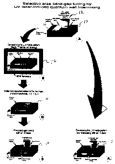
The process of band-gap shifting achieved with an UV laser-induced quantum
well
z o intermixing is schematically described in Figs. 1 A to 1 E.
Figure lA illustrates the process of UV inradiation of a QW sample with an
excimer laser
(308, 248 or 193 nm) or a beam of a high-harmonic of IR laser, such as Nd:YAG
operating at 355 nm or second harmonic Ar-ion laser (244 nm).
Figure 1 B describes the process of developing the UV-made pattern in a Rapid
Thermal
a s Annealing (RTA) furnace.
Figure 1 C indicates a new material that has been obtained following this 2-
step process.
Selectively processed areas of the material may have the band-gap shifted in
excess of
100-200 nm.
CA 02331567 2001-O1-18
Figure 1 D describes the process of fine tuning i_n areas that the initial
intermixing did not
lead to the sufficient band-gap shifting.
Figure I E schematically symbolizes the process of developing the UV-made
pattern (As it
is shown, it can be realized entirely with the use of an IR laser (Nd:YAG or
COZ) as a
heating source).
Figure 2A graphically illustrates that no optical changes (wavelength shift)
occur in the
QW sample following the selective area irradiation with the UV radiation; and
Figure 2B graphically illustrates the evidence of forrrration two selective
areas of band-
gap shifted material following a short-time annealing of the sample that was
first
i o irradiated with the UV radiation.
DETAILED DESCRIPTION OF THE PREFERRED EMBODIMENTS
The present application discloses a novel method for inducing band-gap
shifting as well
as for fine band-gap tuning in III-V semiconductor material microstructures.
The
microstructures of primary interest are quantum-well-based active devices,
such as lasers,
is detectors, amplifies, modulators, etc. Other non-(III-V) material
microstructures, which
comprise quantum wells (QW), e.g., Si/SiGe or CdTe/IriSb, are of interest as
well. By
way of example, and in accordance with the present invention, a QW material 10
to be
tuned is first irradiated with an UV beam 12 and then subjected to thermal
annealing in
furnace 14 (Fig 1 A). The irradiation can be realized with a pulsed laser,
such as excimer
a o or high-harmonic IR laser, or a continuous radiation from an UV lamp
(e.g., an excimer
lamp). The advantage in using an excimer laser is that it can process
relatively large areas
is one step, similarly to the area coverage achieved by the excimer-based
photolithography technique. The purpose of the irradiation is to:
a) introduce defects at the sample surface or in the sub-surface region;
is b) modify the surface of the sample in such a way that it can act either as
a source or sink
of defects that are activated during thermal annealing
The important feature of this method is that the "defect reservoir" 16 created
by the UV
radiation is localized within a shallow depth from the surface, for example,
100 nm or less
and typically 20 nm or less. Also, in addition to the ability to fabricate a
defect-rich layer
CA 02331567 2001-O1-18
near the surface of the irradiated sample, the UV process can be used to
induce chemical
changes and/or the growth of a thin film on top of the processed sample. The
composition
of such film can be chosen to achieve the maximum intermixing effect. The
selective
irradiation of the sample is obtained either by scanning a focused laser beam,
or by
s projecting suitable patterns using a mask technique (projection or contact).
Following
UV irradiation procedure, the sample is thermally annealed (Figs. 1 B, 1 D or
1 E) in order
to realize a defect-mediated process of intermixing between atoms at the
quantum well -
barrier heterointerface. During this step, the intermixing of the well and
barrier material
takes place as a result of a defect-mediated diffusion. The important feature
of this
i o process is that the diffusion occurs at temperatures that are too low to
induce any changes
in areas that had not been exposed to the UV radiation. As a result of the
intermixing the
shape of the quantum well layers is modified, which results in a change of
their ground
state energy levels (band-gap structure). The extent of the intermixing and
modification of
the band-gap structure is controlled by both the composition of the UV-formed
thin film
i s and/or concentration of defects on top of the processed sample. The
process of
intermixing can be achieved is several steps consisting of UV irradiation and
thermal
annealing, which makes it possible to realize a fine band-gap tuning. Both the
process of
UV irradiation and thermal annealing can be carried out in the same chamber,
without
changing the position of the sample, until the required parameters of band-gap
shifting
a o have been achieved.
The sample discussed in Fig. 1 was grown by chemical beam epitaxy. It includes
5
quantum wells of InGaAs that are embedded between InGaAsP barrier layers.
Other QW-
based semiconductor laser materials that could be processed with this
technique include:
AIGaAs/GaAs, AIGaAs/InGaAs, AIGaInP/GaAs. In addition, Si/SiGe QW material
could
as also be processed with this technique.
UV irradiation was carned out with a KrF excimer laser (~, = 248 nm)
delivering 30 ns
pulses. Pulse energy (fluence) at the sample surface was about 100 mJ/cm2. The
results
shown in Fig. 2 concern the photoluminescence measured at room temperature
from the
UV irradiated sample (Fig. 2A) and from the same sample following 10 sec RTA
at 750
3 0 °C. Two sites, which can be seen in Fig. 2B, were irradiated with
500 and 1000 pulses
(site 1 and 2, respectively). The irradiation was carried out using a laser
mask projection
CA 02331567 2001-O1-18
technique, which offers a significant advantage over other techniques applied
for selective
area intermixing, such as ion implantation (the need of a mask being in
physical contact
with the sample) or oxide layer (the surface of the sample has to be patterned
with the
oxide). It can be seen that the UV irradiation alone does not introduce any
changes
s detectable with the photoluminescence mapping (Fig. 2A). Most of the S x 6
mm sample
is characterized by the quantum well signal at ~, = 1505 nm. The sample is
affected only
to a minor extent following a 10 sec annealing at 750 °C, with the
majority of the
background quantum well signal located at ~. = 1499 nm (Fig. 2B). However, two
blue-
shifted areas, each approximately 2.0 x 1.5 mm, of the intermixed material can
clearly be
i o seen in this figure. The 500 (site 1 ) and 1000 (site 2) pulse areas are
characterized by the
quantum well signal at 1476 and 1449 nm, respectively. At this stage, the
sample could be
annealed for the second time in a RTA apparatus, as indicated in Fig. 1 B, or
selected areas
could be annealed with an IR laser, as indicated in Fig. 1D. The use of an IR
laser for fine
tuning makes possible the realization of intermixing in selective areas
without affecting
i5 each other. One skilled in the art may therefore increase the demand for a
material with
band-gap shifted regions that are far beyond limits possible with other
technologies. An
important aspect of the novel tuning method is that the whole process of band-
gap tuning
can be realized with the "laser only" approach. This is schematically
illustrated by the
step A - E in Fig. l .
a o The novel approach exemplified above simplifies the whole procedure of
band-gap
tuning, allows for the application of a more efficient in-situ diagnostics,
leading to a more
efficient, precise and, potentially, less expensive process. The invention
also allows the
processing of industrial size semiconductor wafers 3 inch diameter and more.
It is to be understood that the above description is intended to be
illustrative, and not
2s restrictive. Many other embodiments will be apparent to those skilled in
the art.