Note: Descriptions are shown in the official language in which they were submitted.
CA 02331733 2000-11-06
WO 99/57552 PCT/US99/09500
SENSOR PACKAGING HAVING AN INTEGRAL ELECTRODE PLUG
MEMBER
BACKGROUND OF THE INVENTION
FIELD OF THE INVENTION
This invention relates generally to a method and apparatus for packaging
sensors
and more particularly to chemical sensors, such as pH sensors, where a
microelectronic
substrate, such as an ion sensitive field effect transistor (ISFET), is
integrally packaged
with a counter electrode.
DISCUSSION OF THE RELATED ART
Various ion sensitive field effect transistors (ISFETs), or microelectronic
ion
sensors, are known in the art. Such ISFETs have advantages for use as pH
sensors such
as being solid state, small size and relatively inexpensive to produce.
While semiconductor technology affords the opportunity of fabricating small
sensors, reduced physical size introduces significant packaging challenges. An
ISFET
die includes multiple conductors, which may be routed to external electronic
components. Traditional semiconductor packaging design employs electrical
contact
structures, such as wire bonds, that are made on the same side of the die as
the chemical
sensing ISFET. Because the sensing ISFET is wetted by the measurement sample,
it is
critically important to isolate these ISFET electrical contacts from the test
liquid sample,
particularly when ISFET sensors are operated over a broad range of
temperatures and
pressures. A first step in obtaining package integrity is to locate contact
regions on the
ISFET die backside as taught by Baxter in US Patent No. 4,505,799. While this
is an
important first step, silicon possesses uniquely different chemical and
physical
properties, such as a low value of thermal expansion coefficient in comparison
with
encapsulation polymer materials, which renders it difficult to develop and
maintain
isolation to process sample over sensor lifetime.
CA 02331733 2000-11-06
WO 99/57552 PCT/US99/09500
-2-
Additional techniques to enhance integrity, in the immediate vicinity of the
ISFET die, are described in US Patent No. 5,068,205. In this known technique,
shown
in Figure 1 A, a glass header 12 has been utilized wherein the silicon die
(ISFET) 17 is
adhered to a first side 14 of a borosilicate glass carrier 16 over a through-
hole 15
therein. The carrier 16 has a through-hole 15 in it to maintain uncovered the
contact
areas of the ISFET 17. The carrier 16 also has leads, collectively 18, on the
second side
20 thereof to provide electrical access to the ISFET area from the edges of
the carrier.
The ISFET substrate 17 is electrostatically bonded to the glass carrier 14.
Lead wires,
collectively 22, are then bonded between the ISFET and the glass carrier
leads. The
glass carrier leads 18 and back of the ISFET 17 are then covered with an
insulating
cover 24 for protection. As shown in Figure 1 B, this header assembly 12 is
then
connected to a flexible circuit 26 for leading out through the probe body 28.
This
header 12 and circuit 26 assembly are then enclosed within the probe body 28
along
with a "J"-shaped Hastelloy counter electrode 27, as detailed in US Patent No.
4,851,104, and potted with a thermoset polymer to isolate the internal
components from
the typically corrosive liquids of the sensing environment.
Certain other problems arise in utilizing the ISFET as a practical solution
for
low-cost sensing applications. Among these is the encapsulation of the device
in a body
or housing suitable for utilizing the ISFET as part of an ion-sensitive probe
for
commercial purposes. Typically, the ISFET illustrated in Figure 1 A is potted
in a
thermoset polymer so that the sensor electronics are not subjected to the
often severe
environment of the liquid being tested. Effective thermoset polymer
encapsulation
involves sophisticated assembly processes to obviate voids and to prevent
coating of the
active ISFET surface. These processes are constrained by the working life of
the
uncured thermoset polymer. On completion of the filling operation, thermoset
polymers
typically require additional time for the material to cure.
These aforementioned ISFET sensors are particularly useful when employed in
potentiometric electrochemical measurement systems as probes in making pH
measurements in industrial environments. In many instances earth-grounded
solutions
are subject to noise pickup due primarily to parasitic leakage currents
flowing from the
CA 02331733 2000-11-06
WO 99/57552 PCT/US99/09500
-3-
grounded solution through the measuring electrodes, the associated instrument
or
analyzer and through the analyzer power supply to the instrument ground. In
cases
where AC and DC voltages exist between the solution and instrument grounds,
currents
can be expected to flow via the lowest impedance pathway. This path usually
involves
unwanted current flow through the measurement liquid sample and the
electrodes'
lowest impedance path, which typically is the reference electrode. These
problems are
specially egregious in measurement samples of high purity water of 25
conductivity
values of 10?Siemens/cm or less. These spurious currents offset or shift the
pH reading
and cause drift in the sensor output with a commensurate drift in the
measurement
system accuracy. In order to offset and minimize these spurious currents and
their
undesirable effects, an additional electrically conductive electrode, or
counter electrode,
is inserted into the solution being measured in order to channel the spurious
currents
through this lower impedance electrode rather than through the reference
electrode. The
counter electrode is usually constructed of a electrically conductive material
that is
connected to the measurement system electronics and serves the function of the
metallized gate in a metal oxide field-effect transistor (MOSFET); namely, it
is the
primary electrode to enable FET drain voltage and/or drain current control. A
better
understanding of the counter electrode's function within a potentiometric
electrochemical measurement systems may be had by reference to United States
Patent
No. 4,851,104 to Connery et al.
While the counter electrode technology offers sensor performance benefits, the
use of a metallic or alloy material for the counter electrode would provide a
location of
possible liquid intrusion into the sensor, causing electrical leakage between
internal
electrode conductors, resulting in sensor malfunction. This intrusion is
primarily due to
the significantly different physical properties between the counter electrode
and the
housing and the dissimilar thermal expansion coefficients between these
materials.
Design techniques to achieve sensor package integrity entail employing layered
levels of protection to provide isolation of sensor conductors and sample
fluid. These
include backside contact, an electrostatically bonded intermediate structure
followed by
potting into a sensor subassembly. While this design technique provides for
package
CA 02331733 2000-11-06
WO 99/57552 PCT/US99/09500
-4-
integrity, it is complex, resulting in assembly costs which are in direct
proportion to
design and processing complexity.
Hence, there is need for an ion-sensitive microelectronic sensor package which
is easily and inexpensively contained in an impervious housing while
permitting media
access to the ISFET sensor by effectively sealing the probe electronics from
the media
environment. Additionally, there is a need for packaging techniques that
integrate a
counter electrode in the sensor housing while eliminating the drawbacks of
thermoset
encapsulation.
Certain techniques for encapsulating piezoresistive pressure transducers with
a
conductive elastomeric seal are detailed in US Patent No. 5,184,107 to Maurer.
This
patent details a low cost piezoresistive pressure transducer utilizing pre-
molded
elastomeric seals in which at least one seal is electrically conductive. A
piezoresistive,
stress-sensitive element in the form of a diaphragm of semiconductor material
having a
thickened rim is held at its rim between a pair of pre-molded elastomeric
seals in a two-
piece housing. Electrical connections with external circuitry are made by
conductive
paths through one of the elastomeric seals, which makes contact with
electrical leads
that pass through the housing wall.
BRIEF SUMMARY OF THE INVENTION
Therefore, there is provided by the present invention a chemical sensor
apparatus
and method of making same that is easily and inexpensively manufactured. An
ion-
sensitive microelectronic substrate, or die, is manufactured which has an ion-
sensitive
first surface and patterned electrical leads on its second surface. The die is
placed
between two elastomeric seals, a first media seal, and a second conductive
seal. This
"sandwich" is then loaded, or placed under pressure, within a media-impervious
housing
having a media through-hole therein. A PCB containing patterned electrical
leads
communicates electrically with the die through the selectively conductive
second
elastomeric seal. The first media seal through-hole communicates with the
housing
media through-hole, thereby exposing the ion-sensitive surface of the ISFET
while
CA 02331733 2000-11-06
WO 99/57552 PCT/US99/09500
-5-
protecting the other components of the sensor. A plug constructed of an
electrically
conductive plastic material is then used to mechanically load the PCB, the
elastomeric
seals and the ISFET in position within the probe housing. The plug also makes
an
electrical connection to the PCB during mechanical loading and forms an
integral
counter electrode for the sensor apparatus. The plug is arranged to make a
mechanical
closure with the housing in such a fashion as to form a substantially flush
outer wall
with the housing and to press the media seal into a position permitting media
access to
the ISFET sensor and a hermetic seal of the sensor apparatus electronics from
the media
environment, thereby eliminating the need for thermoset polymer potting.
By simplifying the ion sensitive pH sensor design and integrating the counter
electrode component as part of the sealing mechanism of the apparatus, great
advantages
are attained in reliability while substantially lowering the overall cost of
the probe.
BRIEF DESCRIPTION OF SEVERAL VIEWS OF THE DRAWINGS
The features and advantages of the present invention will be apparent from the
following description of a preferred embodiment thereof, taken in conjunction
with the
sheets of drawings, in which:
Figures 1 A and 1 B are representations of a known ISFET sensor.
Figure 2 is a partial cut-away perspective view of the sensor probe according
to
the present invention.
Figure 3 is a cross-sectional view of a partially completed sensor probe
according to the present invention.
Figure 4 is an exploded view of the media seal, microelectronic structure,
conductive seal, and PCB of the present invention.
CA 02331733 2000-11-06
WO 99/57552 PCT/US99/09500
-6-
Figure 5 is a cross-sectional of the sensor probe before having the internal
components installed.
Figures 6 and 7 are a cross-sectional view and a top-perspective view of the
plug
member and housing of the present invention, respectively.
Figure 8A is a cross-sectional view of a completed sensor probe according to
the
present invention.
Figure 8B is a cross-sectional view of the completed sensor probe of Figure 8A
after hermetically sealing the plug member.
DETAILED DESCRIPTION OF THE INVENTION
Throughout the Description of the Preferred Embodiment, like components will
be identified by like reference numerals.
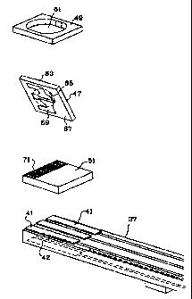
Referring to Figure 2, a sensor apparatus, taught here in the context of a pH
sensor probe 31, has a ISFET housing 33 containing a media through-hole 35
therein.
The housing 33 is composed of any thermoplastic engineering grade plastic
suitable for
the intended sensing environment. Extending from the ISFET housing 33 is a
printed
circuit board 37 ending at its distal end in electrical conductors 39. The
printed circuit
board 37 makes electrical connection between electrical conductors 39 and the
ISFET
(not shown) through printed wiring runs 41 located on a first side of PCB 37.
The
ISFET housing 33 and PCB 37 extend through the length of the pH sensor probe
31 to
join with the outer body 43. The outer body 43 is made of a material selected
to
withstand the type of media environment to which the probe is to be exposed.
As seen in the schematic cross section views of Figure 3 and Figure 5, the
microelectronic ISFET housing 33 is a substantially cylindrical-shaped housing
with the
media through-hole 35 on a first side thereof and an opposing through-hole 45
of a
substantially larger size to permit placement therethrough of the
microelectronic die of
CA 02331733 2000-11-06
WO 99/57552 PCT/US99/09500
-7-
the ISFET 47, the media seal 49 and conductive seal 51 as further explained
below. The
PCB 37 is further contained within the ISFET housing 33, as is plug member 53.
The
plug member 53 is shown in an intermediate or in-work position prior to
completion of
the assembled and sealed ISFET housing.
Plug member 53 is composed, in this preferred embodiment, of a 20% to 40%
graphite-filled, engineering-grade thermoplastic or plastic material, to be
electrically
conductive, and forms thereof a pH insensitive electrode or counter electrode
of the pH
sensor probe 31. The conductive plug member 53 makes electrical contact at
surface 54
with printed wiring runs 42, located on a second side of the PCB 37. An
electrical field
is thus generated at the conductive plug member 53, thereby forming a counter
electrode
that eliminates the need for the separate "J"-shaped Hastelloy counter
electrode 27
shown exiting the body at Figure 1B and a counter electrode that has a
substantially
similar thermal expansion coefficient as the ISFET housing 33. As can be
appreciated
by those skilled in the art, the conductive plug member 53 forms an integral,
one-piece,
electrode plug member that: i) serves to provide a counter electrode that is
in close
proximity to the ISFET sensor, providing therefor the best possible position
to capture
spurious AC and DC currents before they affect the ISFET; and ii) serves to
mechanically lock and seal the principal components of the pH sensor probe 31
within
ISFET housing 33.
The central bore 55 of the ISFET housing 33 is enlarged at the proximal end 57
to provide a nesting cavity 59 for containment of the ISFET 47 and elastomeric
seals 49
and 51. The cavity 59 communicates with the media hole 35. The back hole 45
opposite the media hole 35 also communicates with the central bore 55,
allowing the
electrode plug member 53 to contact the PCB 37, forcing it into contact with
the
conductive sea151 when the electrode plug member 53 is press fit in locking
engagement with ISFET housing 33.
Referencing Figure 4, the principal internal components of the pH sensor probe
31: media sea149, ISFET die 47, conductive seal 51 and PCB 37 with its printed
wiring
runs 41 and 42 are shown, from top to bottom, in the order of their placement
inside
CA 02331733 2000-11-06
WO 99/57552 PCTIUS99/09500
-8-
ISFET housing 33 (not shown). The media sea149 is sized to have its side walls
fit in
abutting contact with the walls of the nesting cavity 59. The media seal 49
has a central
through-hole 61 for alignment with the media hole 35. The media seal is
composed of
an elastomeric material, impervious to the media into which the sensor is
designed to be
immersed. It is understood that media seal hardness and compression is
selected to
provide an effective seal for intended use in the chemical environment over a
broad
range of temperatures and pressures. For example, ethylene propylene diene
monomer
(EDPM) of 50-60 durometer with 10% to 35% compression is used in the presently
contemplated best mode. It should be noted, that even though an elastomeric
material is
used herein to compose the media seal, it will be well understood by those
skilled in the
art that other materials and techniques can be substituted such as gaskets,
sealing
compounds or the like, that are conformable so as to provide a hermetic seal
between
the sensor apparatus electronics and the media environment.
The ISFET die 47 is designed to abut the media seal 49 on a first side 63
thereof,
which contains the ISFET sensing area 65 conditioned to be ion sensitive to
the media
to be sensed. A second side 67 of the die contains patterned electrical leads
69 as
necessary for the operation of the ISFET. Abutting the second side 67 of the
die 47 is
an elastomeric conductive seal 51 commercially known as a "silver stacks
connector"
with conductive silver strips 71 placed therein to allow electrical conduction
in the Z
axis, i.e., through the thickness of the conductive seal, thereby providing
electrical
connection between the die 47 and the printed wiring runs 41 of the PCB 37
when the
components are loaded in opposition to each other within the ISFET housing
(not
shown).
Referring again to Figures 3 and 4, it can be seen that the media seal 49 is
placed
in the nesting cavity 59 which communicates with the media hole 35, with a
major plane
face of the seal substantially parallel to the long axis of the central bore
55. The ISFET
47 is then placed in the nesting cavity 59 in contact with media seal 49 so
that its ion
sensing area 65 is aligned with the media seal through-hole 61, placing the
patterned
electrical lead 69 of the second ISFET surface 67 towards the central bore 55.
Elastomeric conductive seal 51 is then placed in the nesting cavity 59 so that
its silver
CA 02331733 2000-11-06
WO 99/57552 PCT/US99/09500
-9-
conductive strips 71 contact the patterned electrical leads 69 of the ISFET
47. The
elastomeric conductive seal 51 in its unloaded state rests slightly above the
collar 73 of
cavity 59 in its unloaded state. The PCB 37 is then inserted through the
central bore of
the ISFET housing 33 above the conductive seal 51. The PCB 37 is then tipped
down to
preload the seals 51 and 49 and the die 47 therebetween to the predetermined
depth
and/or compression of the collar 73. While the PCB is in this position, the
electrode
plug member 53 is inserted through back hole 45 and is mechanically engaged in
a
press-fit manner to the ISFET housing 33 while pressing the PCB 37 in loading
contact
with the conductive sea151. The electrode plug member 53 includes extended
shoulder
areas 52 that engage in a frictional fit against interior surfaces 36 of ISFET
housing 33.
The electrode plug member 53 is inserted into back hole 45 until landing
projections 57
rest on surfaces 48. As can be seen in Figure 8A, when fully seated within
back hole
45, electrode plug member 53 provides a substantially flush outer wall that
seals the
ISFET body 33 in the area of back hole 45 and forms a hermetic seal between
ISFET
housing 33 and the ISFET die 47 via the media seal 49. It has been found that
a
compression force of approximately 10% to 35% is sufficient to seal the ISFET
die 47
against the housing 33, thereby preventing the media environment from entering
into the
interior of ISFET housing 33 and the internal components of the pH sensor
probe.
Flush mounting of the electrode plug member is preferred where the probe is to
be
inunersed in a flowing liquid, but is not considered a necessity for mating
the plug
member and housing outside surface in all embodiments of the present
invention. All
internal electrical components are locked in place with the elastomeric seals
providing
the necessary cushioning for the ISFET to prevent breakage thereof during
mechanical
operations.
The present invention further includes means for hermetically sealing the
electrode plug member 53 from the media environment when the sensor is
contemplated
to be used in a high-temperature and -pressure operating environment.
Referencing
Figures 5, 6 and 7, it can be seen that the ISFET housing back hole 45 has a
integral
circumferential collar 75 extending outwardly from the outer edge of a
shoulder 83,
extending between the back hole 45 and the collar 75. The back hole 45 and its
area
leading to the central bore 55 are shaped to accept and secure in a press-fit
manner the
CA 02331733 2000-11-06
WO 99/57552 PCT/US99/09500
-10-
electrode plug member 53 (Figure 6). The electrode plug member 53 is radiused
at its
outside surface 77 to be substantially similar to the radius of the outside
wall of ISFET
housing 33, which is of a substantially cylindrical shape. Extending from the
outside
surface 77 of the electrode plug member 53 is an integral circumferential
collar 79.
Once the electrode plug member 53 is press fit into ISFET housing back hole
45,
the circumferential collar extensions of each member are aligned with a space
therebetween comprising a well 85 between the collar extensions 75, 79 whose
bottom
is the shoulder 83. A heat seal anvil 87 of the proper radius to serve as a
molding
element for the desired final shape, in this case flush and cylindrical, is
then brought
down to melt the housing and plug collar members together. As can be seen in
Figure
8B, the collar material then melts and flows into the well 85, whereupon the
anvil 87 is
brought to below melt temperature to set the plastic and then removed, thereby
providing a substantially flush outer wall with a hermetic seal in the back
hole area of
the ISFET housing 33. In the preferred embodiment, the plug collar 79 is
designed to
melt away from the electrode plug member 53 and blend with the body material
to
ensure that conductive thermoplastic material remains at the surface 77.
Relief areas 89
are further provided in the housing body as a catch basin for collar melt
material to
maintain a flush housing body outer wall (Figure 8B). It will be well
understood by
those skilled in the art that the heat sealing method just described is one of
many
methods that can be used to provide a hermetic seal of conductive plug member
53 to
ISFET housing 33, such as employing material fusion techniques using lasers,
ultrasonics, radiant heat or the like. Additionally, hermetic sealing may also
be
accomplished by the application of a liquid or semi-liquid sealing compound
within
relief areas 89 to effectively form a hermetic seal and, therefore, the
invention is not
limited thereto.
The present invention has been described with particular reference to the
preferred embodiments thereof. It will be obvious that various changes and
modifications can be made therein without departing from the spirit and scope
of the
invention as defined in the appended claims.