Note: Descriptions are shown in the official language in which they were submitted.
CA 02331970 2001-O1-19
['!~'~ ~
SILICON PLATFORM FOR OPTICAL MODULES
FTETD OF THE INVENTION
The present invention relates to a silicon platform for
optical modules, which has a conductor pattern formed on a silicon
substrate.
BACKGROUND OF THE INVENTION
In an optical communication system or optical data
communication system, an optical module incorporating optical
elements such as laser diodes is used. This optical module is now
installed in homes along with recent progress made in computer
hardware and communication networks. Thereby, demand for
small-sized, highlyintegrated andlow-costopticalmodulesarises.
To meet such demand, the development of the following optical
module is under way. The optical module comprises a substrate on
which optical elements such as light emitting elements and
light-receiving elements and a conductor pattern are formed in a
package and is connected to optical fibers or optical waveguide
component for communication.
The substrate constituting the optical module is preferably
a silicon substrate. The reason for this is that silicon (Si) has
excellent workability. Therefore, for example, the silicon
substrate has such an advantage that it is easy to put alignment
1
CA 02331970 2001-O1-19
marks for position determination on the silicon substrate when
optical elements are to be mounted or to form V-shaped grooves for
the position determination of optical fibers in the silicon
substrate when the optical fibers are to be arranged.
Further, silicon has excellent heat radiation properties.
Therefore, the silicon substrate has such an advantage that it can
serve as a heat sink for radiating heat from optical elements. The
silicon substrate has a further advantage that a raw material for
the manufacture of the silicon substrate can be acquired at a low
cost and has stable quality.
The silicon substrate having the advantages, on which optical
elements, a conductor pattern and optionally the alignment marks
and V-shaped grooves are formed is called "silicon platform for
optical modules."
Fig. 5 shows a typical example of the silicon platform for
optical modules. The silicon platform for optical modules shown
in Fig. 5 has a silicon substrate 505 and an Si02 insulating layer
507 which is an oxide layer formed on the silicon substrate 505.
A light-receiving element 501 and a light emitting element 504 all
of which are optical elements are mounted on the Si02 insulating
layer 507 through a conductor pattern 506. A microstrip line
structure is formed on the Si02 insulating layer 507 at a position
other than the area for mounting the optical elements 501 and 504.
This microstrip line structure is a laminate consisting of a ground
2
CA 02331970 2001-O1-19
film 510, a dielectric film 509 and signal lines (conductor pattern)
508, all formed in the order named.
The conductor pattern 506 formed in the area for mounting the
optical elements 501 and 504 and the signal lines 508 of the
microstrip line structure are electrically connected to each other
by lead wires 502. Thereby, the optical elements 501 and 504 are
electrically connected to the signal lines 508 by the conductor
pattern 506 and the lead wires 502.
The silicon substrate 505 has a thickness of about 1 mm, for
example. The dielectric film 509 is made from polyimide, for
example. This dielectric film 509 has the function of insulating
the ground film 510 from the conductor pattern 508.
The silicon platform for optical modules shown in Fig. 5 is
constituted as described above. A typical example of optical
module comprising this silicon platform for optical modules is shown
in Fig. 6. In Fig. 6, the silicon platform for optical modules is
mounted on a substrate 601. A wiring pattern 602 and lead frames
611 are formed and a part 603 such as a preamplifier IC are mounted
on the substrate 601. External connection terminals are further
provided on the substrate 601 as required.
The substrate 601 having the silicon platform for optical
modules and the part 603 mounted thereon, for example, is
incorporated in a package (not shown) together with an optical
ferrule 613 shown in Fig. 6 to constitute an optical module. The
3
CA 02331970 2001-O1-19
optical ferrule 613 is connected to one ends of optical fibers 612.
The other ends of the optical fibers 612 are drawn out to the outside
of the package. To store the optical ferrule 613 in the package
of the optical module, the optical ferrule 613 is arranged such
that the optical fibers 612 can be optically connected to the optical
elements 501 and 504.
Since the silicon platform for optical modules shown in Fig.
has both the light-receiving element 501 and the light emitting
element 504 as described above, the optical module shown in Fig.
6 comprising the silicon platform for optical modules can be an
optical module for two-way communication.
Both the light-receiving element 501 and the light emitting
element 504 are mounted on the silicon platform for optical modules
shown in Fig. 5 and Fig. 6 as described above. As a matter of course,
there are the following silicon platforms for optical modules
besides the silicon platform. For example, there is a silicon
platform for optical modules, which comprises only one of the
light-receiving element 501 and the light emitting element 504.
As shown in Fig. 7, there is also a silicon platform for optical
modules which comprises an optical array element 701, on which a
plurality of light-receiving elements 501 or light emitting
elements 504 are disposed in an array.
QBJECTS AND SUMMARY OF THE INVENTION
4
CA 02331970 2001-O1-19
The silicon platform for optical modules has such a problem
as the deterioration of transmission signals through the lead wires
502 or signal lines 508 along with an increase in the transmission
speed of signals.
To prevent the deterioration of the transmission signals, it
is necessary to carry out the matching of impedance between the
optical elements 501 and 504 and the signal lines 508. Therefore,
a silicon platform for optical modules is constructed to realize
the matching of impedance between the optical elements 501 and 504
and the signal lines 508 in consideration of the downsizing of the
optical module and crosstalk between adjacent signal lines 508.
However, to this end, the thickness of the dielectric film 509 of
the microstrip line structure must be made very small.
An example will be shown. For example, a case where the
matching of impedance between the light emitting element 501 and
the leader line 508 to be electrically connected to the light
emitting element 501 is carried out will be described hereinafter.
When the serial resistance value of a laser diode which is the light
emitting element 501 is 5 to 10 S2, the characteristic impedance
Zo of the leader line 508 must be set to 5 to 10 S2 which is the
same as the serial resistance value of the light emitting element
501.
To this end, the ratio (H/W) of the thickness H of the
dielectric film 509 underlying the leader line 508 with respect
CA 02331970 2001-O1-19
to the line width W of the leader line 508 must be about 0.06.
When a plurality of optical elements are arranged, in
consideration of the downsizing of the silicon platform for optical
modules (that is, the downsizing of the optical module), these
optical elements are preferably arranged at the same pitch as the
pitch of the optical fibers of the optical fiber tape to be optically
connected to the optical elements. According to the current
standards for the optical fiber tapes, the pitch of the optical
fibers is 250 ~.m.
When the signal lines 508 are arranged according to the
lay-out of the optical elements as shown in Fig. 5, the pitch of
the signal lines 508 is the same as the pitch of the optical elements.
When the pitch of the signal lines 508 and crosstalk between the
adjacent signal lines 508 are taken into consideration, the line
width W of the signal lines 508 is desirably smaller than 100 Vim.
To realize the matching of impedance between the optical
elements and the signal lines 508 while the line width W of the
signal lines 508 is fixed, the thickness H of the dielectric film
509 must be made smaller than about 6 ~m based on the requirement
for the ratio, that is (H/W) - 0.06, of the thickness H of the
dielectric film 509 with respect to the line width W of the signal
lines 508.
However, if the dielectric film 509 is made thin to such an
extent, when the wire 502 is to be bonded to the leader line 508
6
CA 02331970 2001-O1-19
on the dielectric film 509, the dielectric film 509 may be peeled
off by bonding impact and the leader line 508 may be damaged. To
eliminate this problem, the thickness H of the dielectric film 509
must be made 20 to 30 ~.m or more.
However, to realize the matching of impedance between the
optical elements and the signal lines 508 while the dielectric film
509 is made thick, the line width W of the signal lines 508 must
be made large. In addition to this, in consideration of the
above-described crosstalk problem, the pitch of the signal lines
508 must be expanded. Thereby, the silicon substrate must be made
large in size.
That is, the dielectric film 509 is made thick to prevent the
damage of the signal lines 508 caused by the bonding of the wires
502, and the silicon platform for optical modules becomes large
in size to realize the matching of impedance between the optical
elements and the signal lines 508.
It is an object of the present invention which has been made
to solve the problems to provide a silicon platform for optical
modules which can increase the speed of a transmission signal and
can be reduced in size with ease and further can prevent such a
problem as the exfoliation of a conductor pattern (bonding pad
portion) caused by the bonding of wires.
To attain this object and solve the problem, the present
invention is constituted as described below. That is, according
7
CA 02331970 2001-O1-19
to a first aspect of the present invention, there is provided a
silicon platform for optical modules which comprises a silicon
substrate, a first insulating layer formed on this silicon substrate,
a first conductor layer formed on the first insulating layer, a
second insulating layer formed on the first conductor layer and
a second conductor layer formed on the second insulating layer,
an end portion of the second conductor layer overlying the first
insulating layer to constitute bonding portions to be connected
to lead wires.
According to a second aspect of the present invention, in the
first aspect of the invention, the silicon platform is characterized
in that a hole is formed in the second insulating layer and a bonding
portion is formed in this hole.
According to a third aspect of the present invention, in the
first aspect of the invention, the silicon platform is characterized
in that a removed portion is formed in the second insulating layer
and a bonding portion is formed in this removed portion.
According to a fourth aspect of the present invention, in the
first, the second or the third aspect of the invention, the silicon
platform is characterized in that the thickness of the second
insulating layer is 6 ~,m or less.
According to a fifth aspect of the present invention, in the
first or the fourth aspect of the invention, the silicon platform
is characterized in that optical elements are mounted and an end
8
CA 02331970 2001-O1-19
portion of the second conductor layer lies right below the optical
elements.
According to a sixth aspect of the present invention, in any
one of the first to the fifth aspects of the invention, the silicon
platform is characterized in that a bulky portion is formed on part
of the first insulating layer.
According to a seventh aspect of the present invention, in
any one of the first to the sixth aspects of the invention, the
silicon platform is characterized in that the first conductor layer,
the second insulating layer and the second conductor layer
constitute a microstrip line structure.
According to an eighth aspects of the present invention, in
any one of the first to the seventh aspects of the invention, the
silicon platform is characterized in that the second conductor layer
constitutes a coplanar distribution constant circuit structure.
According to a ninth aspect of the present invention, in any
one of the first to the eighth aspects of the invention, the silicon
platform is characterized in that a silicon platform for optical
modules is electrically connected to a driver IC by lead wires.
According to a tenth aspect of the present invention, in any
one of the first to the ninth aspects of the invention, the silicon
platform is characterized in that at least one of a light emitting
element and a light-receiving element are mounted on the silicon
platform.
9
CA 02331970 2001-O1-19
According to an eleventh aspect of the present invention, in
any one of the first to the tenth aspects of the invention, the
silicon platform is characterized in that the first insulating layer
is an oxide layer.
According to a twelfth aspect of the present invention, in
any one of the first to the eleventh aspects of the invention, the
silicon platform is characterized in that the first insulating layer
is an SiOz insulating layer.
According to a thirteenth aspect of the present invention,
in any one of the first to the twelfth aspects of the invention,
the silicon platform is characterized in that the second insulating
layer is a resin film.
According to a fourteenth aspect of the present invention,
in any one of the first to the thirteenth aspects of the invention,
the silicon platform is characterized in that the second insulating
layer is a polyimide film.
According to the present invention, an end portion of the
second conductor layer overlies the first insulating layer to
constitute bonding portions. Bonding strength between the
conductor layer and the insulating layer is higher than bonding
strength between the dielectric film and the oxide layer.
Therefore, such a problem that the bonding pads peel off from the
oxide layer (insulating layer) when the lead wires are bonded to
the respective bonding pads is almost eliminated.
CA 02331970 2001-O1-19
Since the problem that the bonding pads peel off from the oxide
layer rarely arises, the dielectric film can be made thin without
worrying about the problem. Thereby, the size of the silicon
platform for optical modules can be reduced and it is easy to realize
the matching of impedance between the conductor pattern which is
the second conductor layer and the optical elements electrically
connected to the conductor pattern, thereby preventing the
deterioration of transmission signals, and making it easy to
increase the speed of transmission signals.
Use of this silicon platform for optical modules makes it
possible to provide a small-sized and highly integrated optical
module and which is moreover capable of high-speed transmission
of signals at a low cost.
Since the exfoliation of bonding pads occurs in the prior art,
it is necessary to bond wires carefully. In contrast to this, thanks
to the special structure of the present invention, a silicon
platform for optical modules can be manufactured without worrying
about the problem of exfoliation of the bonding pads.
In the structure that the end portion of the second conductor
layer lies right below the optical elements, the optical elements
can be electrically connected to the conductor pattern, which is
the second conductor layer without using lead wires. Thereby, the
problem of the prior art, that is, the exfoliation of the bonding
pads caused by the bonding of the wires does not occur. Therefore,
11
CA 02331970 2001-O1-19
the dielectric film of the microstrip line structure can be made
thin without worrying about the exfoliation of the bonding pads.
This makes it easy to realize the matching of impedance
between the conductor pattern (second conductor layer) and the
optical elements electrically connected to the conductor pattern.
Therefore, a small-sized silicon platform for optical modules,
which prevents the deterioration of transmission signals and is
capable of transmitting signals at high speed, can be provided.
Further, the optical elements and the conductor pattern
(second conductor layer) of the microstrip line structure are
electrically connected to each other without using lead wires.
Therefore, the step of bonding the lead wires for electrically
connecting the conductor patterns can be omitted. Thereby, the
production process can be simplified.
,~RTEF DESCRIPTION OF THE DRAWINGS
These and other objects and advantages of the present
invention will become more apparent and more readily appreciated
from the following detailed description of the exemplary
embodiments of the invention taken in conjunction with the
accompanying drawings, in which:
Fig. la is a sectional view for explaining a silicon platform
for optical modules according to a first embodiment of the present
invention and Fig. 1b is a plan view for explaining the silicon
12
CA 02331970 2001-O1-19
platform for optical modules according to the first embodiment of
the present invention;
Fig. 2a is a sectional view for explaining a silicon platform
for optical modules according to a second embodiment of the present
invention and Fig. 2b is a plan view for explaining the silicon
platform for optical modules according to the second embodiment
of the present invention;
Fig. 3a is a sectional view for explaining a silicon platform
for optical modules according to a third embodiment of the present
invention and Fig. 3b is a plan view for explaining the silicon
platform for optical modules according to the third embodiment of
the present invention;
Fig. 4a is a sectional view for explaining a silicon platform
for optical modules according to a fourth embodiment of the present
invention and Fig. 4b is a plan view for explaining the silicon
platform for optical modules according to the fourth embodiment
of the present invention;
Fig. 5 is a perspective view showing a typical example of
silicon platform for optical modules;
Fig. 6 is a diagram for explaining an example of optical module
comprising the silicon platform for optical modules shown in Fig.
5; and
Fig. 7 is a model diagram showing an example of silicon
platform for optical modules on which a plurality of optical
13
CA 02331970 2001-O1-19
elements disposed in an array are mounted and an example of optical
module comprising the silicon platform.
DETAILED DESCRIPTION OF THE PREFERRED EMBODIMENTS
The present invention will be described in detail hereinafter
with reference to the accompanying drawings of preferred
embodiments.
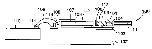
Fig. 1a is a sectional view of a platform for optical modules
according to a first embodiment of the present invention, which
is, connected to a driver IC 110 and optical fibers 111. Fig. 1b
is a plan view of the platform for optical modules of the first
embodiment, which is, connected to the driver IC 110 and the optical
fibers 111 as in Fig. la.
The platform 100 for optical modules of the first embodiment
shown in Fig. la and Fig. 1b has a laser diode array 101 which is
an optical element mounted thereon and signal lines 107 which are
a conductor pattern formed thereon.
That is, the platform 100 for optical modules of the first
embodiment has a silicon substrate 102. This silicon substrate 102
has a thickness of about 1 mm, a width of about 6 mm, a length of
about 3 mm and a resistivity of about 2, 000 S2cm. An Si02 insulating
layer (first insulating layer) 103 which is an oxide layer is formed
on the surface of the silicon substrate 102 by a thermal oxidation
method.
14
CA 02331970 2001-O1-19
A wiring pattern 104 is formed in an area for mounting the
laser diode array 101 (optical element mounting area) on the SiOz
insulating layer 103. This wiring pattern 104 is a conductor
pattern made from copper or gold and the laser diode array 101 is
mounted on this wiring pattern 104.
In this first embodiment, as shown in Fig. la and Fig. 1b,
the optical fibers 111 are connected to an end portion of the silicon
platform 100 for optical modules. The laser diode array 101 emits
light toward the optical fibers 111 and is optically coupled with
the optical fibers 111. For example, the laser diode array 101
consists of 6 end emission type laser diodes disposed in an array
and comprising a resonator made of a double-hetero structure InGaAsP
active layer formed on an InP substrate. Each of the light emitting
diodes has an oscillation wavelength of 1.31 ~.m and a threshold
current of 5 mA. The wiring pattern 104 is formed in accordance
with the lay-out of the light emitting elements.
The laser diode array 101 is mounted in an area on the end
side of the silicon substrate 102 on which the optical fibers 111
are provided to carry out optical coupling between the laser diode
array 101 and the optical fibers 111. V-shaped grooves for the
position determination of the optical fibers 111 are formed in the
silicon substrate 102 and an optical ferrule is provided at the
end portions of the optical fibers 111. The V-shaped grooves and
the ferrule are not shown in Fig. la and Fig. 1b.
CA 02331970 2001-O1-19
As shown in Fig. la and Fig. 1b, a ground film 105 which is
a first conductor layer and a microstrip line structure are formed
on the Si02 insulating layer 103 at a position other than the optical
element mounting area. As shown in Fig. la, this microstrip line
structure is a laminate consisting of the ground film (first
conductor layer) 112, a dielectric film (second insulating layer)
106 and the signal lines (second conductor layer) 107 which is a
conductor pattern, all formed in the order named. In this first
embodiment, the signal lines 107 of the microstrip line structure
are arranged in accordance with the lay-out of the optical elements
of the laser diode array 101.
Bonding pads 108 (108a, 108b) for connecting the lead wires
109 are formed on both end portions of the signal lines 107. The
bonding pad 108a on one end side of the signal lines 107 is connected
to respective bonding pads 114 formed on the driver IC 110 shown
in Fig. la and Fig. 1b by lead wires 109. The bonding pads 108b
on the other end side of the signal lines 107 are electrically
connected to the wiring pattern 104 by lead wires 109 as shown in
Fig. 1b.
The wiring pattern 104, ground films 105 and 112, dielectric
film 106 and signal lines 107 are formed to predetermined patterns
by deposition and a lift-off method using photolithography.
In this first embodiment, the dielectric film 106 is a resin
film (for example, a polyimide film) and has a thickness of about
16
CA 02331970 2001-O1-19
2 Vim, for example.
This first embodiment is characterized in that it has a
structure capable of preventing the occurrence of such a problem
that the bonding pads 108 peel off when the lead wires 109 are to
be bonded to the bonding pads 108.
That is, as shown in Fig. la, a hole (removed portion) 113
is formed in the dielectric film 106 of the microstrip line structure
at a position for the formation of the bonding pad 108. This hole
113 is a hole extending from the surface of the dielectric film
106 to the Si02 insulating layer 103. This hole 113 is formed by
removing part of the dielectric film 106 by the patterning of the
dielectric film 106. A conductor material is directly formed on
the Si02 insulating layer 103 exposed to the bottom of this hole
113. This conductor material is connected to the leader line 107
and constitutes the bonding pad 108.
According to this first embodiment, the bonding pads 108 are
directly formed on the Si02 insulating layer 103. Bonding strength
between the conductor material and the Si02 insulating layer is
higher than bonding strength between the dielectric film and the
SiOz insulating layer. Therefore, such a problem that the bonding
pads 108 made from a conductor material peel off from the Si02
insulating layer 103 when the lead wires 109 are bonded can be almost
suppressed. Thereby, the dielectric film 106 can be made thin
without worrying about the exfoliation of the bonding pad 108.
17
CA 02331970 2001-O1-19
In this first embodiment, the line width of the signal lines
107 is made small (for example, about 70 Vim) and the interval between
the adjacent signal lines 107 is made narrow in consideration of
a reduction in the size of the silicon platform 100 for optical
modules and crosstalk. In addition, the dielectric film 106 can
be made thin without worrying about the exfoliation of the bonding
pads 108 . Therefore, it is easy to realize the matching of impedance
between the signal lines 107 and the optical elements 101 by reducing
the thickness of the dielectric film 106. Thereby, high-speed
transmission of signals can be realized while the deterioration
of the transmission signals is prevented.
Therefore, this first embodiment can provide such an
excellent effect that a small-sized silicon platform for optical
modules which enables high-speed transmission of signals can be
provided by the special constitution.
A second embodiment of the present invention will be described
hereinafter. In this second embodiment, the present invention is
applied to a silicon platform 201 for optical modules which does
not have any optical elements mounted thereon, as shown in the
sectional view of Fig. 2a and the plan view of Fig. 2b. That is,
the silicon platform 201 for optical modules of this second
embodiment is such as shown in Fig. 2a and Fig. 2b that it is provided
between the silicon platform 100 for optical modules of the first
embodiment and the driver IC 202 and electrically connects the
18
CA 02331970 2001-O1-19
optical elements of the silicon platform 100 for optical modules
to the driver IC 202. As the silicon platform 100 for optical
modules has already been described in the section of the first
embodiment, its description is omitted in this second embodiment.
In the silicon platform 201 for optical modules of this second
embodiment, an Si02 insulating layer (first insulating layer) 206
which is an oxide layer is formed on the surface of a silicon
substrate 203. A microstrip line structure is constructed on this
Si02 insulating layer 206. This microstrip line structure is a
laminate consisting of a ground film 207 which is a first conductor
layer, a dielectric film (for example, a polyimide film) 211 which
is a second insulating layer, and signal lines (second conductor
layer) 205 which are a conductor pattern, all formed in the order
named. On both end sides of the signal lines 205 of this microstrip
line structure, bonding pads 208 (208a, 208b) are provided.
In the example shown in Fig. 2a and Fig. 2b, the bonding pads
208a on one end side of the signal lines 205 are electrically
connected to the respective bonding pads 212 of the driver IC 202
by lead wires 209. The bonding pads 208b on the other end side of
the signal lines 205 are connected to the respective bonding pads
108a of the silicon platform 100 for optical module of the first
embodiment by lead wires 209.
This second embodiment is characterized in that it has a
special structure for preventing such a problem as the exfoliation
19
CA 02331970 2001-O1-19
of the bonding pads 208 caused by the bonding of the lead wires
209 like the first embodiment.
That is, as shown in Fig. 2a, a hole 213 extending from the
surface of the dielectric film 211 to the SiO~ insulating layer 206
is formed in the dielectric film 211 of the microstrip line structure
at a position for the formation of the bonding pad 208. A conductor
material is directly formed on the Si02 insulating layer 206 exposed
to the bottom of the hole 213. This conductor material constitutes
the bonding pad 208 electrically connected to the leader line 205.
According to this second embodiment, like the first
embodiment, the bonding pad 208 is directly formed on the Si02
insulating layer 206 by forming the hole 213 in the dielectric film
211 of the microstrip line structure at the position for the
formation of the bonding pad 208. Bonding strength between the
conductor material constituting the bonding pad 208 and the Si02
insulating layer is higher than bonding strength between the
dielectric film 211 and the SiOz insulating layer 206. Therefore,
such a problem that the bonding pads 208 peel off from the SiOz
insulating layer when the lead wires 209 are bonded to the respective
bonding pads 208 is almost prevented.
As described in the section of the first embodiment, the
dielectric film 211 can be made thin without worrying about the
exfoliation of the bonding pads 208. As a result, the second
embodiment can provide such an effect that a small-sized silicon
CA 02331970 2001-O1-19
platform for optical modules which enables the high-speed
transmission of signals can be provided at a low cost.
A third embodiment of the present invention will be described
hereinafter. In the embodiments, the optical elements (laser diode
array) 101 are mounted on the silicon platform 100 for optical
modules. In contrast to this, in this third embodiment, the present
invention is applied to a silicon platform for optical modules on
which a light emitting element and a light-receiving element are
both mounted.
Fig. 3a is a sectional view of the silicon platform for optical
modules according to this third embodiment. Fig. 3b is a plan view
of the silicon platform for optical modules according to the third
embodiment.
In this silicon platform 300 for optical modules of the third
embodiment, an Si02 insulating layer (first insulating layer) 305
which is an oxide layer is formed on the surface of a silicon
substrate 303. A light emitting element 301 and a light-receiving
element 302, both of which are optical, elements are mounted on
the Si02 insulating layer 305 through wires 304, which are a
conductor pattern. A microstrip line structure is formed on the
Si02 insulating layer 305 at a position other than the area for the
formation of the optical elements 301 and 302. This microstrip line
structure is a laminate consisting of a ground film (first conductor
layer) 307, a dielectric film (second insulating layer ) 309, and
21
CA 02331970 2001-O1-19
signal lines (second conductor layer) 308 which is a conductor
pattern, all formed in the order named as shown in Fig. 3a.
On both end sides of the signal lines 308 of the microstrip
line structure, bonding pads 310 (310a and 310b) are provided. The
bonding pads 310a on one end side of the signal lines 308 are
electrically connected to the driver IC shown in the embodiments
by lead wires . The bonding pads 310b on the other end side of the
signal lines 308 are electrically connected to the wires 304 by
lead wires 311 as shown in Fig. 3b. Thereby, the optical elements
301 and 302 are electrically connected to he above signal lines
308 through the wires 304, the lead wires 311 and the bonding pads
310b.
This third embodiment is characterized by the special
structure of the bonding pads 310 like the embodiments. That is,
as shown in Fig. 3a, a hole 312 extending from the surface of the
dielectric film 309 to the SiOz insulating layer 305 is formed in
the dielectric film 309 of the microstrip line structure at a
position for the formation of the bonding pad 310. A conductor
material is directly formed on the Si02 insulating layer 305 exposed
to the bottom of the hole 312. This conductor material constitutes
the bonding pad 310 electrically connected to the leader line 308.
Since the bonding pads 310 are formed in this third embodiment
like the embodiments, the same effect as in the embodiments can
be provided.
22
CA 02331970 2001-O1-19
A fourth embodiment of the present invention will be described
hereinafter. In this fourth embodiment, such a problem as the
exfoliation of the bonding pads is eliminated by a special structure
different from that of the embodiments. Fig. 4a is a sectional view
of a silicon platform for optical modules according to the fourth
embodiment. Fig. 4b is a plan view of the silicon platform for
optical modules according to the fourth embodiment.
In this fourth embodiment, like the third embodiment, an Si02
insulating layer 405 which is a first insulating layer is formed
on the surface of a silicon substrate 403. A light emitting element
401 and a light-receiving element 402 which are optical elements
are mounted on the Si02 insulating layer 405 through a conductor
pattern 409 which is a first conductor layer. A microstrip line
structure is formed on the SiOz insulating layer 405 at a position
other than the area for mounting the optical elements 401 and 402.
This microstrip line structure is a laminate consisting of a ground
film 406 which is a first conductor layer, a dielectric film 407
which is a second insulating layer and signal lines (second
conductor layer) 408 which is a conductor pattern, all formed in
the order named as shown in Fig. 4a.
This fourth embodiment is characterized in that the signal
lines 408 of the microstrip line structure and the conductor pattern
409 in the area for mounting the optical elements to be connected
to the signal lines 408 are electrically connected by a connection
23
CA 02331970 2001-O1-19
conductor pattern 410 as shown in Fig. 4a and Fig. 4b.
According to this fourth embodiment, the optical elements 401
and 402 can be electrically connected to the signal lines 408 without
using lead wires. Therefore, bonding pads for connecting the
optical elements 401 and 402 to the signal lines 408 can be
eliminated. As a result, such a problem as the exfoliation of the
bonding padsfor electrical connection between the opticalelements
401 and 402 and the signal lines 408 does not arise.
Also in this fourth embodiment, the bonding pads 412 in the
signal lines 408 of the microstrip line structure have the same
structure as in the embodiments. That is, a hole is formed in the
dielectric film 407 and the bonding pad 412 is directly formed on
the SiOz insulating layer 405.
Since the silicon substrate 403 has excellent heat radiation
properties, it can serve as a heat sink for radiating heat from
the optical elements 401 and 402. However, when the Si02 insulating
layer 405 on the surface of the silicon substrate 403 is made thick,
the efficiency of head transfer from the optical elements 401 and
402 to the silicon substrate 403 worsens. Therefore, the Si02
insulating layer 405 is desirably made as thick as about 500 nm.
However, when the conductor portion is directly formed on the
Si02 insulating layer 405 like the connection wiring pattern 410
and the bonding pads 412, parasitic capacitance is produced between
the conductor portion and the silicon substrate 403. Therefore,
24
CA 02331970 2001-O1-19
when the Si02 insulating layer 411 is made thin in consideration
of the heat radiation properties of the optical elements 401 and
402, parasitic capacitance between the conductor portion and the
silicon substrate 403 becomes very large. Such large parasitic
capacitance affects high-frequency transmission signals, thereby
deteriorating high-frequency characteristics.
To solve this problem, in this fourth embodiment, a bulky
portion 411 is formed on the SiOz insulating layer 405 at a position
for the formation of the connection conductor pattern 410 and a
position for the formation of the bonding pad 412. This bulky
portion 411 expands the interval between the conductor portion and
the silicon substrate 403, thereby reducing parasitic capacitance
between the conductor portion and the silicon substrate 403.
Thereby, the deterioration of the high-frequency characteristics
can be prevented.
The bulky portion 411 can be formed as follows. For example,
the Si02 insulating layer 405 is formed on the surface of the silicon
substrate 403 to a thickness of 2 ~,m, for example, by thermal CVD.
Thereafter, the thickness of the Si02 insulating layer 405 except
the area for the formation of the bulky portion 411 is reduced to
500 nm, for example, by photolithography and etching. Thus, a thin
film portion and the bulky portion 411 can be formed on the Si02
insulating layer 405.
In the fourth embodiment, heat radiation from the optical
CA 02331970 2001-O1-19
elements 401 and 402 can be improved by reducing the thickness of
the Si02 insulating layer 405 in the area for mounting the optical
elements 401 and 402. In addition, the bulky portion 411 is formed
on a portion for the formation of the conductor portion of the SiOz
insulating layer 405 except the area for mounting the optical
elements 401 and 402. Therefore, the deterioration of high-
frequency characteristics can be prevented as described above.
The present invention is not limited by the embodiments and
can be embodied in various ways . For example, in the embodiments,
the optical elements mounted on the silicon platform for optical
modules are directly connected to optical fibers. For example,
planar waveguides (PLC) may be mounted on a silicon platform for
optical modules and the optical elements may be indirectly bonded
to the optical fibers through the PLC.
In the embodiments, the conductor pattern formed on the
silicon platform for optical modules constitutes the microstrip
line structure. For example, a conductor pattern constituting a
coplanar distribution constant circuit may be mounted on a silicon
platform for optical modules.
Further, in the embodiments, the present invention is applied
to a silicon platform for optical modules on which a light emitting
element, or both of a light emitting element and a light-receiving
element are mounted. As a matter of course, the present invention
can be applied to a silicon platform for optical modules on which
26
CA 02331970 2001-O1-19
only a light-receiving element out of the light emitting element
and light-receiving element is mounted.
Further, the constitution of an optical module comprising the
platform for optical modules is not limited to those shown in Fig.
6 and Fig. 7. The optical module comprising the platform for optical
modules is various in constitution. The silicon platform for
optical modules to which the present invention is applied may be
incorporated in any one of the optical modules.
27