Note: Descriptions are shown in the official language in which they were submitted.
CA 02332209 2001-O1-24
Atty. Docket No. I 2229
WIRE BOND PAD AND METHOD THEREFOR
BACKGROUND OF THE INVENTION
The invention relates generally to conductors. having wire bond pads to
which conductive leads of integrated circuit dice are connectable and methods
therefor.
Wire bonding is a known technique for mounting electrical circuit devices,
for example semiconductor integrated circuit dice, in electronic packaging.
These circuit
devices generally comprise a plurality of relatively small conductive leads
that are
electrically -connected, for exa~rrrpte by ultrasonic bonding, to wire bond
pads of
I 0 corresponding conductors embedded in the device package, which is usually
a dielectric
material. See generally U.S. Patent.No. 5,463,255 entitled "Semiconductor
Integrated
Circuit Device Having an Electrode Pad Including an Extended Wire Bonding
Portion"_
In some applications, the conductive leads or wires of the circuit devices are
bonded to aluminum pads formed on corresponding conductors of the device
package.
I 5 In a known aluminium wire bond pad forming operation, a channel is formed
in a strip .of
stock conductor material, for example a copper alloy, and a relatively thin
strip of
aluminum inlay is disposed in the channel. Thereafter, the conductor material
with the
aluminum inlay is reduced in a cold rolling operation to approximately one-
half its original
thickness. The conductor material with the inlayed aluminum strip is then cut
into
20 individual conductors strips, each of which includes an aluminum portion,
which forms the
wire bond pad The aluminum inlay material used in known aluminum wire bond pad
forming operations, however, is ,available from a limited supp:fy and is very
costly.
An object of the present invention is to provide novel wire bond pads and
methods therefor the overcome problems in and improve upon the prior art.
25 Another object of the invention is to provide novel wire bond pads and
methods therefor that are economical and reliable.
A further object of the invention is to provide novel wire bond pads and
CA 02332209 2001-O1-24
"Wire Bond Pad And Method 'therefor" Atty. Docket No. 12229
methods therefor that utilize reduced amounts of wire bond pad material.
Another object of the invention is to provide novel wire bond pads fortr~ed
by conducting members disposed in openings of corresponding conductors
embeddeel in
an insulating member of a circuit device package.
A more particular object of the invention is to provide novel wire bond pads
for electrical circuit device packages generally comprising a conductor of a
first electrically
conductive material embedded in an insulating member, preferably by insert
molding, and
a conducting member of a second electrically conductive material disposed in
an opening
of a portion of the conductor protruding into a device accommodating portion
of the
electrical circuit device package.
Another more particular object of the invention is to provide novel wire bond
pad methods generally comprising forming an opening in a conductor of a first
electrically
conductive material, forming a conducting member of a second electrically
conductive
material, transferring the conducting member into the opening of the
conductor, and
electrically contacting the conducting member with the conductor.
These and other objects, aspects, features and advantages of the present
invention will become more fully apparent upon careful consideration of the
following
Detailed Description of the Invention and the accompanying Drawings, which may
be
disproportionate for ease of understanding, wherein like structure and steps
are referenced
generally by corresponding numerals and indicators.
BRIEF DESCRIPTION OF THE DRAWINGS
FIG. 1 is a partial view of an electrical device having conductive leads
bonded to corresponding wire bond pads of a device package>.
FIG. 2 is a process flow diagram for forming a wire bond pad on a
conductor.
2
CA 02332209 2001-O1-24
"Wire Sond Pad And Method Therefor" Atty. Docket No. 12229
FIG. 3 is a schematic diagram for forming a wire bond pad on a conductor.
DETAILED (DESCRIPTION OF THE INVENTION
FIG. 1 illustrates a an electrical circuit device package 10 generally
comprising an insulating member 12 having one or more electrical device
accommodating
portions, which are in the exemplary form of recessed cavities or openings ~I4
formed in
the insulating member, for accommodating electrical circuit devices 20, for
example
semiconductor dice.
The device package 10 also comprises one or more conductors 30 of a first
electrically conductive material embedded in the insulating member 12, and in
one
preferred embodiment the conductors 30 are insert molded into the insulating
member,
which is formed of a plastic or some other moldable material suitable for
circuit device
packaging applications.
In PIG. 1, portions 32 of the one or more conductors 30 protrude from the
insulating member I2 into the circuit device accommodating portion 14 thereof
for
coupling to corresponding electrical leads or conductors 22 of the circuit
device 20, as
discussed below.
The conductors 30 and particularly the portion, 32 thereof protruding into
the device accommodating portion of the device package 10 include
corresponding
openings each having a conducting member 40 of a second electrically
conductive material
disposed therein and in electrical contact therewith. The conducting members
40 thus
form the wire bond pads to which the electrical Leads 22 from the circuit
device 20 are
electrically coupled, for example by ultrasonic bonding and other processes
know to those
of ordinary skill in the art.
In one embodiment, the opening is a hole extending through conductor
portion 32, and the conducting member 40 is a generally cylindrical stud or
blank
disposed therein and electrically coupled thereto, for example 6~y a stamping
or some other
3
CA 02332209 2001-O1-24
"Wire Bond Pad And Method Therefor" Atty. Docket No. 12229
operation, as discussed more fully below.
In one embodiment, the conductor 30 and the portion 32 thereof protruding
into the device accommodating recess is copper alloy and the conducting member
40 that
forms the wire bond pad is aluminum. In alternative embodLiments, the
conductor 30 and
the conducting member 40 are formed of other conducting materials.
FIG. 2 is a process flow diagram for forming a wire bond pad an a
conductor comprising generally forming an opening in a conductor of a first
electri<:aliy
conductive material in a forming operation 50, forming a conducting member in
a blanl{ing
operation 52, transferring the conducting member into the opening in a
transferring
operation 54, and electrically contacting the conductor and conducting member
in a
contacting operation 56. Although these various operations are illustrated in
the i~low
diagram as being performed separately, one more of the operations may be
performed
simultaneously.
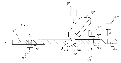
In FIG. 3, the opening is formed in the conductor, for example a copper
strip 100, by punching a hole 102 therethrough with a hole forming punch I I
0. 'The
opening may be formed alternatively by some other operation, for example a
drilling; or
milling operation, and need not extend fully through the conductor. The
conductor strip
I 00 is generally moved in a feed direction to and from the punch 110 or other
opening
forming station.
In some embodiments, a bevel I 04 is formed about the opening I 02 on one
or both sides of the conductor strip 100. The bevels I 04 may be formed by the
punch
I I 0 during the hole forming operation, or thereafter by dedicated bevel
forming machinery
120, for example in a stamping or drilling or milling operation.
In FIG. 3, the conducting member 40 is formed from a second conducaor
I 06, for example an aluminum strip, that is fed generally non-parallel to the
feed direcnion
of the conductor strip I 00. In the exemplary embodiment, the conducting
member 40 is
formed as a blank or slug with a blanking punch 130. In the one preferred
embodiment,
the blank 40 is transferred into the opening I 02 by the blanking punch I 30
as the blank
4
CA 02332209 2001-O1-24
"Wire Bond I'ad And Method 'Therefor" Atty. Docket No. 12229
40 is formed.
The transferring of the blank 40 by the blanking punch 130 also forms the
electrical contact between the blank 40 and the conductor 100. In some
alternative modes
of manufacture, the blank 40 is subject to further stamping or other
operations which
further improves the electrical contact with the conductor.
In the exemplary embodiment wherein the hole 102 includes the one: or
more bevels 104, the axial dimension of the blank 40 is grE~ater than that of-
the opening
I 02 so that the blank protrudes from the sides of the conductor 100 having
the bevels
104, as illustrated in FIG. 3. Thereafter, the one or more portions of the
blank 40
protruding from the opposite sides of the conductor are sfamped by a
flattening punch
140, which flattens or reduces the blank toward the surface level of the
conductor, tl'rus
filling the beveled portion 104 of the conductor with the material of the
conducting
member or blank.
The flattening of the protruding portions of the: conducting member or blank
40 and the resulting configuration thereof increases the contact surface area
between the
flattened blank 42 and the conductor 100, and also provides increased wire
bond pad
surface area for a given amount of blank conductor maten;-ial, thereby more
efficiently
utilizing the material that forms the wire bond pad.
In another alternative operation, the conductor strip 100 with ahe
conducting members 40 may be subject to a rolling operation, either instead of
or after
the flattening operation. The rolling operation however is not required,
although it may
be desirable for some conductor applications where further reduction in strip
thickness
and/or more robust electrical contact between the blanks an<l the conductor
are required.
The conductor strip and particularly the flattened conductor members .42
thereof are preferably polished in a polishing operation, and are cut into
individual
conductors suitably sized for embedding into device packages, as illustrated
generally in
FIG. I .
While the foregoing written description of the invention enables one of
5
CA 02332209 2001-O1-24
"Wire Bond Pad And Method Therefor" Atty. Docket No. 12229
ordinary skill fo make and use what is considered presently to be the best
mode thereof,
those of ordinary skill will understand and appreciate the existence of
variations,
combinations, and equivalents of the specific exemplary embodiments herein.
'The
invention is therefore to be limited not by the exemplary embodiments herein,
but by all
embodiments within the scope and spirit of the appended claims.
6