Note: Descriptions are shown in the official language in which they were submitted.
CA 02332537 2000-11-20
GAS DISCI-IARGE LAMP BASE WITH A STARTING DCVICI:
This invention relates to a gas discharge lamp base with a starting device
according to the
preamble of Claim 1.
Such a gas discharge lamp base with a starting device is known from U.S.
Patent 5,510,967 A. In
the case of the gas discharge lamp base known from U.S. Patent 5,510,967 A, a
tubular jacket
section of the gas discharge lamp is pressed into the gas discharge lamp base
by means of a
slotted ball. Two contact bars arranged inside the gas discharge lamp base
guarantee electric
contact of the electric current lead-in wire and the current return wire with
the respective
terminals of the starting device. According to U.S. Patent 5,510,967 A, the
starting device has a
compact design in the four of an elongated cylinder which extends inside the
gas discharge lamp
base pcipendicular to the longitudinal extent of~the gas discharge lamp.
However, precise details
regarding the intc~mal structure of the starting device cannot be obtained
from U.S. Patent
5,510,967 A.
A similar gas discharge lamp base is known from U.S. Patent 5,659,221 A, but
instead of the
slotted ball, a slotted truncated conical wedge is used to establish the press
comiection according
to U.S. Patent 5,659,221 A.
German Patent Application 196 10 385 A also describes a gas discharge lamp
base with a
starting device. According to German Patent Application 196 10 385 A, two
electric terminals of
the starting device, a first winding of a trigger pulse transformer and the
two main electrodes of
the gas discharge lamp are connected in series. In addition, the two electric
temoinals of the
starting device arc connected to one another by a series connection of a
capacitor across an
ohmic resistor. A series connection of a second winding of the starting pulse
transfouner with a
spark gap is connected in parallel with the capacitor. The starting impulse
transfooncr and the
CA 02332537 2000-11-20
additional electronic components mentioned above, the electric terminals
mentioned above, part
of the gas discharge vessel and part of the outer line running along the gas
discharge vessel are
completely or partially sheathed or cast with a plastic material to fornl the
gas discharge lamp
base.
German Patent Application 195 41 438 A describes a gas discharge lamp with a
starting device
where the high voltage-carrying components of the starting device are arranged
in the lamp base,
while the low voltage-carrying components are arranged in the lamp socket.
U.S. Patent 5,838,109 A discloses a starting device for a discharge lamp with
a starter circuit and
a noise filter circuit. However, this starting device is not arranged in a
lamp base.
German Patent Application 196 10 388 A discloses another gas discharge lamp
base with a
starting device. 'the starting device according to German Patent Application
196 10 388 A has a
high voltage capacitor and a Tesla transformer. The two latter components are
arranged in such a
way that the high voltage capacitor is surrounded by the secondary coil of the
Tesla transformer.
The object of this invention is to provide a gas discharge lamp base with a
starting device having
improved operational reliability in comparison with the known gas discharge
lamp bases.
According to this invention, this object is achieved by a gas discharge lamp
base with a starting
device according to Claim 1.
In the case of the gas discharge lamp base with a starting device according to
this invention, the
improved operational reliability is achieved through complete spatial
separation of the high
voltage-carrying components from the low voltage-carrying components, with all
these
components nevertheless being accommodated in the gas discharge lamp base so
that the gas
discharge lamp base need not be connected to a power supply over a high
voltage interface but
instead can be connected over a low voltage interface. With regard to the
definition of terms, it
should be pointed out that "low voltage" is understood here to refer to a
voltage of up to a few
2
CA 02332537 2000-11-20
kV. In contrast with that, the term "high voltage" here refers to a voltage
above approximately 10
kV, in particular a voltage of a few tens of kV.
Advantageous and preferred embodiments of the gas discharge lamp base
according to this
invention are the object of Claims 2 through 17.
The special three-dimensional arrangement of the interference suppression
coils) according to
Claim 4 with respect to the direction of gas discharge contributes to an
especially good
electromagnetic compatibility of the gas discharge lamp base with a starting
device according
this invention.
The embodiment according to Claim 6 guarantees especially good high voltage
isolation and
thus an especially good operational reliability.
The labyrinth obtained in the case of the embodiment according to Claim 11 in
conjunction with
the top part of the housing and the carrier part forms a longer path for any
creep current that may
occur and is therefore an especially effective insulation measure which
contributes toward an
improvement in operational reliability in an advantageous manner. The same
thing is also true of
the embodiment according to Claim 14 with respect to the bottom part of the
housing.
In the case of the embodiment according to Claim 17, the high voltage strength
of the gas
discharge lamp base is improved due to the closed outer contour of the gas
discharge lamp base,
and the thermal load-bearing capacity of the electric components arranged in
the gas discharge
lamp base is reduced due to the radiant heat emitted by the gas discharge, and
failure of the
components contained in the gas discharge lamp base is prevented.
The planar conductor frame (also called a lead frame) according to Claim 18
offers the
advantage that the terminals can be welded in one plane at the time of
manufacture. The lead
frame also offers other advantages: thicker circuit board conductors than in
the case of printed
CA 02332537 2000-11-20
circuits, a greater strength of the carrier due to the plastic-sheathed
circuit board conductors, and
the creep paths can be lengthened by integrally molded ribs.
After assembly of the components on the high voltage side of the carrier part,
its walls are treated
with a so-called primer which ensures a good bond between the inside wall of
the high voltage
space and the casting compound introduced subsequently. This primer is poured
into the high
voltage compartment and is poured out again immediately. Nevertheless, primer
can still
penetrate into the bushings for the terminal wires. To prevent this, the
partition between the high
voltage side and the low voltage side of the carrier part should be absolutely
tight. However, this
cannot be achieved in the case of terminal wires passing through boreholes.
The embodiment according to Claim 19 remedies this situation because the
connection between
the bottom of the earner part and the metal tube on the one hand and the
contacting of the ends
of the tubes on the circuit board conductors on the other hand can be designed
to be tight in a
reliable manner.
The embodiment according to Claim 20 facilitates the insertion of the terminal
wires of the
components of the high voltage side into the metal tubes.
The embodiment; according to Claim 21 facilitates the insertion of the tubes,
which are fixedly
connected to the bottom of the carrier part, into the holes provided in the
circuit board
conductors of the lead frame. In addition, by means of a protrusion of the
edges of the holes in
welding, a reserve of material is made available.
The joint welding of the ends of the tubes to the respective terminal wire and
the circuit board
conductor permit, an absolutely tight seal (Claim 22).
In addition, the metal tubes also have the function of securing the lead frame
after welding,
optionally supported by lugs provided on the top part of the carrier.
4
CA 02332537 2000-11-20
Finally, the metal housing according to Claim 23 surrounding the lamp base has
the advantage of
good shielding with respect to the outside. It is irrelevant here how the
interference suppression
coils are arranged with respect to the gas discharge burning in the gas
discharge vessel.
Embodiments of the gas discharge lamp base with a starting device according to
this invention
are explained below on the basis of figures, which show:
Figure 1: an embodiment of a gas discharge lamp base according to this
invention with the
respective gas discharge lamp in a cross-sectional view from the side,
partially
dismantled, without electronic components;
Figure 2: an embodiment of the gas discharge lamp base according to this
invention with
the electronic components installed and the respective gas discharge lamp in
an
exploded diagram shown from the side;
Figure 3: the embodiment from Figure 2 shown in a perspective exploded
diagram;
Figure 4: an embodiment of a carrier part for electronic components of a
starting device in
the gas discharge lamp base according to this invention, shown in a plan view
from above;
Figure S: section C-C from Figure 4;
Figure 6: the; carrier part from Figure 4 seen as a plan view from beneath;
Figure 7: section F-F from Figure 6;
Figure 8: an embodiment of a housing top part of the gas discharge lamp base
according to
this invention, shown in a side view;
CA 02332537 2000-11-20
Figure 9: the top part of the housing from Figure 9, shown in plan view from
beneath;
Figure 10: an embodiment of a bottom part of a housing of the gas discharge
lamp base
according to this invention, shown in a perspective view;
Figure 11: an embodiment of a circuit arrangement of the starting device with
the gas
discharge lamp connected;
Figure 12: a second embodiment of a gas discharge [lamp] base according to
this invention
in a perspective exploded diagram;
Figure 13: a perspective diagram of a carrier part with the lead frame mounted
on it;
Figure 14: the essential parts of the base from Figure 12 in an exploded
diagram shown from
the side;
Figure 15: a partial section of the bottom of the carrier part and the lead
frame;
Figure 16: the top and bottom parts of a metal housing enclosing the base; and
Figure 17: the schematic diagram of a second embodiment of a circuit
arrangement of the
starting device with the gas discharge lamp connected.
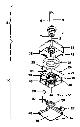
Figures 1 through 3, each in different types of diagrams, illustrate an
embodiment of a gas
discharge lamp base 1 according to this invention with a starting device, but
the components
belonging to the starting device have been omitted in Figure 1. This also
shows the respective
gas discharge lamp 2, whose gas discharge vessel 3 with gas discharge
electrodes 4, outer
plunger 5, current return wire 7, partially sheathed with a ceramic tube 6,
and inner current lead-
in wire 8 and an inside base part 9 form one structural unit which is mounted
in a housing top
part 10 of the gas discharge lamp base and adjusted there.
6
CA 02332537 2000-11-20
Housing top part 10 (see also Figures 8 and 9) has electrically insulated
bushings or openings 13,
14 for the inner current lead-in wire 8 and the current return wire 7.
Additional isolating webs
11, 12 on the housing top part 10 improve the electric insulation between the
current return wire
7 and the inner current lead-in wire 8.
Gas discharge lamp base 1 according to this invention also has a carrier part
16 for electronic
components of the starting device (see also Figures 4 through 7). The carrier
part 16 is provided
with form-fitting receptacles 17 through 20 for the bushings 13, 14 and the
isolating webs 11, 12
of the housing top part 10. This forms a labyrinth for any creep currents that
might occur. The
entire starting device (electronic starter) for the gas discharge lamp 2 is
mounted in the carrier
part 16. The carrier part 16 together with the electronic components of the
starting device is
inserted into the housing top part 10, where it is locked in place by means of
catches 21 which
engage in corresponding recesses 22 on the inside walls of housing top part
10.
Carner part 10 has a top side and a bottom side and is fitted on both sides
with the components
of the starting device. The terms "top side" and "bottom side" are not
necessarily to be
interpreted as smooth sides. As illustrated in Figures 1 through 7, each side
may have its own
steps. However, the top side and the bottom side are separated from one
another so that it is
impossible to go from one of these two sides to the other without having to
pass over an outer
edge 31 of the carrier part 16 or through one of the two bushing holes 19, 20
located inside the
inner receptacle wall 17.
Carrier part 16 is assembled in such a way that the components of the starting
device carrying a
high voltage (approx. 30 kV) are arranged on one side of the carrier part 16,
and the components
of the starting device carrying a low voltage (approx. 2 kV) are arranged on
the other side of
carrier part 16.
In particular, an ignition transformer, which is designed as a toroidal core
transformer 23
(Figures 2, 3), two interference suppression coils 23, 25 and one high voltage
capacitor 26 are
located on the high voltage side of carrier part 16. These high voltage-
carrying components 22
7
CA 02332537 2000-11-20
through 26 are embedded in an electrically insulating casting compound. The
two interference
suppression coils 24, 25 are located across the direction of the gas discharge
burning in the
respective gas discharge vessel 3 to achieve the best possible electromagnetic
compatibility of
the entire arrangement. In the present embodiment, the two interference
suppression coils 24, 25
are also mounted in particular across the longitudinal extent of gas discharge
lamp 2.
On the side facing away from the high voltage side of the carrier part 16,
namely the low voltage
side of the carrier part 16, are arranged a spark gap 27, a starting capacitor
28, an interference
suppression capacitor 29 and an ohmic resistor 30. Heat-sensitive parts are
arranged at the
greatest possible distance from the gas discharge vessel 3.
Walls 31, 17 of the carrier part 16 form cast compartments on the one hand and
also serve as
electric insulation on the other hand. In addition, the carrier part 16 has
additional compartments
for punched bending metallic insert parts 32 to 38. The punched bending
metallic insert parts 32
to 38 establish electric contact with the inner current lead-in wire 8 and the
current return wire 7
and are provided with U-shaped brackets for contacting wires, in particular
for connecting wires
of electronic components 27 through 30. The wires are welded to the punched
bending insert
parts 32 to 38, i.e., no circuit board is used but instead the electronic
design is based on the lead-
frame technology.
Carrier part 16 is also provided with a collar space 39 which serves to
accommodate a plug of a
connecting cable. The connecting cable connects the starting device to the
remaining
components, which are accommodated in a separate operating device, of the
circuit arrangement
which is necessary for operation of the lamp.
The embodiment of gas discharge lamp base 1 according to this invention with
the starting
device illustrated here is also provided with a housing bottom part 40 (see
Figures 1 through 3
and 10). Housing bottom part 40 has electrically insulating webs and walls 41,
42 which engage
in a form-fitting manner in corresponding receptacles 43, 44 of the carrier
part 16 (see Figure 6).
This forms a labyrinth of insulation walls, creating elongated pathways for
any creep currents
CA 02332537 2000-11-20
that might occur and thus contributing toward a guarantee of especially good
operational
reliability of gas discharge lamp base 1 according to this invention with the
starting device as
illustrated as an embodiment.
Housing top part 10 is provided with integrally molded pins or lugs 15 which
extend in guide
grooves 46 of the carrier part 16 and pass through corresponding openings 45
in the housing
bottom part 40, where they are ultrasonically welded to the housing bottom
part 40. In other
embodiments of the gas discharge lamp base 1 according to this invention, the
housing top part
and housing bottom part 40 are laser welded together at the periphery or are
locked together
peripherally or in segments.
Housing top part 10, the carrier part 16 and the housing bottom part 40 in the
embodiment
described here are each made of an electrically insulating plastic which can
withstand high
thermal loads. The operating temperature in the gas discharge lamp base 1 may
amount to up to
150EC with this choice of materials. In the embodiment illustrated here, the
gas discharge lamp
base according to this invention has a closed outer contour in the assembled
state. The resulting
special advantages have already been explained above.
The electric circuit design of a starting device will now be explained briefly
with reference to
Figure 11.
In this embodiment, the starting device is a so-called asymmetrical pulse
starting device. Of the
three d.c. voltage terminals 47, 48, 49, optionally two are used. The d.c.
voltage terminal 49 is at
ground and leads over a resistor 25 to a terminal 51 of the gas discharge lamp
2. The d.c. voltage
terminal 47 is for a power supply voltage of !400 V, and d.c. voltage terminal
48 is for a power
supply voltage of +600 V. The starting capacitor 28 is discharges in bursts
over a spark gap 27
and over the primary winding N1 of starting transformer 23. The discharge
current flowing
through the primary winding N1 of starting transformer 23 induces unipolar
high voltage pulses
of a positive or negative polarity, depending on the power supply voltage
used, in the secondary
winding N2 of starting transformer 23. The inner current lead-in wire 8 of the
gas discharge lamp
9
CA 02332537 2000-11-20
2 receives these high unipolar voltage pulses at terminal 15. The starting
voltage pulses in the
present embodiment have an amplitude of approximately 25 kV and a pulse width
of
approximately 300 ns. High voltage capacitor 26 is connected in parallel to
the discharge path of
gas discharge lamp 2.
The embodiment of the gas discharge lamp base according to this invention as
illustrated in
Figures 12 through 14 essentially resembles those described above. The base
consists of the
essential components: a housing top part 10, a carrier part 16 and a bottom
part 40. The essential
changes in comparison with the first embodiment are to be found in the lead
frame 60, which
carnes the spark gap 27, the capacitors 28, 29, the resistor 30 and a
threshold switch 52 (Figure
17), the additional partition 61 on the housing bottom part 40 and the contact
strap 63 and the
base contact 64.
Figure 13 shows the carrier part 16 after assembly of the lead frame 60 with
the low voltage-
carrying components of the base. As illustrated in this diagram, all the
contacts are arranged in a
plane, thus greatly facilitating welding of the contacts.
As shown in Figure 14, the base contact 64 connects the inner current lead-in
wire 8 to a terminal
of the toroidal core transformer. The contact strap 63 connects the current
return wire 7 of the
gas discharge lamp to the interference suppression coil 24. The additional
labyrinth partition 61
serves to shield the contact strap 63 from the low voltage-carrying components
on the lead frame
60. As shown in this figure, the toroidal core transformer (together with the
other high voltage-
carrying components of the base) is cast in a casting compound 62.
Figure 15 shows a partial section of the partition 16N of the carrier part 16.
Beneath this wall are
the high voltage-carrying components of the base on the lead frame 60, and
above this wall are
the low voltage-carrying components of the base on the lead frame 60. A tube
made of metal
such as copper is injected or pulled into the partition 16N and the connection
between the two is
absolutely tight. The lead frame 60 arranged above the partition 16N consists
essentially of the
circuit board conductors 70, which are sheathed by insulating plastic. There
are holes at the
CA 02332537 2000-11-20
contact points protruding upward, i.e., toward the side facing away from the
high voltage-
carrying side. The metal tubes 71 are inserted into these funnel-shaped
protrusions. The terminal
wires 72 are in turn inserted into the metal tubes, which are widened in a
funnel shape on the
high voltage side. After welding the ends of the terminal wires 72 to the ends
of the tubes 71 and
the protrusions of the circuit board conductors 70, a tight weld is obtained,
guaranteeing a
reliable seal between the two sides of the carrier bottom 16.
Figure 16 illustrates a metal housing consisting of two halves, the top part
80 and the bottom part
81 and surrounds the base 1 on all sides. This yields a reliable shielding of
the base, in which
case it does not matter where the interference suppression coils 24, 25 are
positioned.
Figure 17 illustrates the schematic diagram of a second embodiment of the
starting device with
the gas discharge lamp 2 connected. This circuit arrangement differs from that
illustrated in
Figure 11 by a bidirectional threshold switch 52 which is connected to
terminal 47 on the one
end and to terminal 51 on the other end, i.e., it is connected in parallel to
capacitor 29 and
resistor 25, so that the schematic diagram of this threshold switch
corresponds to two Zener
diodes connected in series and in the opposite directions. Such a threshold
switch is distributed
by the company SGS Thompson under the brand name Transil~ diode. As an
alternative, the
threshold switch 52 may also be connected to ground instead of being connected
to terminal 51.
The high voltage-carrying components and the low voltage-carrying components
are each
bordered with a dotted line and are labeled as H [high] and N [low].
11