Note: Descriptions are shown in the official language in which they were submitted.
R. Barnett 1-7-19-10-3 - 1 -
SHEET-METAL FILTER
Technical Field
This invention relates to high-frequency, e.g., microwave,
filters.
s Background of the Invention
The recent proliferation of, and resulting stiff competition
among, wireless communications products have put price/performance
demands on filter components that conventional technologies find difficult
to deliver. This is primarily due to expensive manufacturing operations
~o such as milling, hand-soldering, hand-tuning, and complex assembly.
Summary of the Inyention
This invention is directed to solving this and other problems and
disadvantages of the prior art. According to the invention, a filter is made
from a single sheet of electrically conductive material, e.g., metal,
15 preferably by stamping. The sheet may either be all metal, e.g., a metal
plate, or it may be a metal-laminated non-conductive substrate, e.g., a
printed-circuit board. In the latter case, the filter may advantageously be
made by etching. An electrically conductive housing preferably
encapsulates at least both faces of the sheet. The sheet of conductive
2o material defines a frame, one or more resonator filter elements inside of
the frame, and one or more supports attaching the resonators to the
frame. At least one contact connected to the resonator filter element
provides an electromagnetic contact thereto. Preferably, the contact is a
flange on at least one of the resonators, also defined by the sheet of
2s conductive material. Another flange or the frame itself serves as another
contact to the filter. Illustratively, the flanged resonator is rectangular
and
the flange and the supports extend from a side of the rectangle, whereby
the distance between the flange and an end of the rectangular resonator
CA 02332758 2001-O1-30
R. Barnett 1-7-19-10-3 - 2 -
that lies on the same side of the supports as the flange primarily
determines the input characteristics of the filter.
Major benefits of the invention include low manufacturing costs,
narrow (illustratively about 1 %) bandwidth filters requiring no tuning, and
s high Q, relative to conventional technology. These and other features and
advantages of the invention will become more evident from the following
description of an illustrative embodiment of the invention considered with
the drawing.
Brief Description of the Drawing
1o FIG. 1 is a perspective view of a filter that includes a first
illustrative embodiment of the invention;
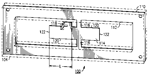
FIG. 2 shows illustrative dimensions of the resonant element of
the filter of FIG. 1;
FIG. 3 is a graph of first operational characteristics of the
1s resonant element of FIG. 2;
FIG. 4 is a graph of second operational characteristics of the
resonant element of FIG. 2;
FIG. 5 is a perspective view of a filter that includes a second
illustrative embodiment of the invention;
2o FIG. 6 is a perspective view of a filter that includes a third
illustrative embodiment of the invention; and
FIG. 7 is a perspective view of a filter that includes a fourth
illustrative embodiment of the invention.
Detailed Description
2s FIG. 1 shows a first bandpass filter 100, which comprises an
electrically conductive (e.g., metallic) filter element 110 positioned inside
a
cavity formed by an electrically conductive housing 104. The cavity is
dimensioned to exhibit a waveguide cutoff frequency below the
frequencies at which filter 100 is being used. Filter element 110 is a single
so sheet of electrically conductive material, such as a sheet of aluminum or
CA 02332758 2001-O1-30
R. Barnett 1-7-19-10-3 - 3 -
steel, or a metal-coated (laminated) substrate, such as a printed-circuit
board. In the latter case, the printed-circuit may be metal-coated on both
sides, with one of the sides forming a part of housing 104. In the case of
being a single sheet of metal, filter element 110 is easily manufactured by
stamping. In the case of being a laminate, filter element 110 is easily
manufactured by etching. Cutting or other manufacturing methods may
also be used. Filter element 110 need not be planar. Outer portions
thereof may be bent substantially perpendicularly to the rest to form a part
of the walls of housing 104. Filter element 110 comprises a frame 112, a
~o resonator 114 inside of frame 112, supports 116 connecting resonator 114
to frame 112, and a coupler 118; a second contact is formed by frame 112
and supports 116. While coupler 118 is shown in FIG. 1 as a contact
flange extending from resonator 114, coupler 118 can be a button coupler
or an out-of-side coupler, or a capacitive coupler, or any other desired
coupler. Flange 118 may extend from resonator 114 in the plane of filter
element 110' through a gap 270 in frame 112, as shown in FIG. 5. This
planar configuration of filter element 110' possesses up-down symmetry
which achieves automatic suppression of waveguide modes in filter 100.
As a consequence, the cut-off frequency of filter 100 is pushed up high,
2o and the filter achieves very good suppression of second harmonics.
However, flange 118 may be bent away from the plane of filter
element 110, as shown in FIG. 1, to extend outside of housing 104
through an opening 120 therein to form a connectorless coupling to, e.g.,
an antenna. The bent-up flange 118 destroys the up-down symmetry of
2s filter element 110' and hence destroys the suppression of the waveguide
modes. In order to regain the high suppression of second harmonics, the
bent-up flange 118 must be positioned at an integer multiple of half-
wavelengths of the second harmcr,ic frequency of the filter's center
frequency from the inside edge of frame 112. Preferably, both frame 112
3o and resonator 114 are rectangular in shape, and flange 118 and
CA 02332758 2001-O1-30
R. Barnett 1-7-19-10-3 - 4 -
supports 116 extend from the long sides 120 (as opposed to the short
ends 122) of resonator 114.
For a bandpass half-wavelength filter, the important parameters
are the loaded Q of the end resonators forming the coupling to the filter,
the center frequency of each resonator, and the inter-resonator coupling
coefficients. They can be calculated for the specific type of filter that is
desired. Electromagnetic (EM) simulations are used to relate these
parameters to the specific structures and physical dimensions of the
resonators for realization of the filter, because it is usually very difficult
if
io not impossible to solve the problems analytically due to the complexity of
the studied structures. The dimensions of an illustrative endcoupling
resonator 114 are shown in FIG. 2. The dimension "L" between the edge
of flange 118 that is closest to support 116 and an end 122 of
resonator 114 that lies on the same side of support 116 as flange 118 is
~5 critical in that it is determinative of the input/output characteristics of
filter 100 and the loaded Q of the input/output resonators. The
relationship of the loaded Q and center frequency f o to the parameter L is
determined by simulations, whose results are shown in FIG. 3 as
curves 210 and 220. Simulations provide an invaluable means to study
2o and optimize the overall structures through exploration of an enormous
design space, which might be otherwise impossible. However, due to
inaccuracy in EM modeling, several prototypes with dimensions close to
those selected by simulations were built and measured to map out the
exact dependence experimentally for fine adjustment to achieve a no-
25 tuning design. Their results are also shown in FIG. 3 as curves 230
and 24. It is clear from FIG. 3 that the desired loading Q and the center
frequency may not coincide with each other. However, variation of the
resonator's length, such as lengthening or shortening both ends by the
same amount, will only affect the center frequency but not the Q. Hence,
so desired Q and center frequency can be achieved simultaneously.
CA 02332758 2001-O1-30
R. Barnett 1-7-19-10-3 - 5 -
FIG. 6 shows a third filter 300, which comprises an electrically
conductive filter element 310 mounted inside an electrically conductive
housing 304. Filter element 310 is also a single sheet of material, and
comprises five resonators 311-315 (coupled at their adjacent edges
across gap G) to form a five-pole filter. Resonators 311-315 are
positioned inside a frame 312 and are connected thereto by supports 316
and 317. Contact flanges 318 and 319 extend from sides 320 of the two
outermost resonators 310 and 314. Filter element 310 is also easily
manufactured by stamping or etching. Flange 318 is bent away from the
~o plane of filter element 310 and extends outside of housing 304 via
orifice 322 to form a first contact to filter 300. Flange 319 extends outside
of housing 304 through a gap 330 in frame 312 to form a second contact
of filter 300. Suppression of the low-frequency parasitic mode is achieved
by designing the end resonators 311 and 314 properly such that the
~5 center frequency of the parasitic mode of the end resonators 311 and 314
are very different from that of the inner resonators 312, 313, and 315.
For the inner resonators, their center frequencies are mainly
determined by their lengths, approximately inverse-proportionally. The
coupling between the resonators is determined by the gap G between
2o them. Usually the coupling will have a weak effect on the center
frequency, which should be taken into consideration. In general, gap G is
hard to describe by an analytical mathematical formula; fortunately it is not
necessary because the coupling effects can generally be found by
measurement. The measured relationship between gap width G and the
25 coupling coefficient K and center frequency f o for filter 300 of FIG. 6 is
shown in FIG. 4. Coincidentally for this filter 300, the center frequency is
independent of the coupling coefficient, so the desired center frequency
can be achieved by adjusting the resonator length, independently of the
gap width.
3o With all the relevant dimensions mapped out, a desired
frequency response can be achieved at any frequency. In addition to the
CA 02332758 2001-O1-30
R. Barnett 1-7-19-10-3 - 6 -
desired frequency response in the desired bands, a filter will often display
some parasitic modes at the undesired places. They can be reduced or
eliminated on a case-to-case basis by manipulating the structures in a way
that suppresses those undesired modes but not the desired one by
properly engineering the width and the shape of tabs 316 so that they do
not perturb the desired modes of propagation in the resonant elements.
FIG. 7 shows a fourth filter 400, which also comprises an
electrically conductive filter element 410 mounted inside an electrically
conductive housing 404. This design is particularity suited for
1o implementing a transceiver duplexer. Filter element 410 defines dual
side-by-side five-pole filters. Of course, any desired number of filters may
be defined by a single filter element 410. The filters may be cascaded for
better performance. Or, they may be used for different stages of a
transmitter or a receiver. Or, one may be used for the transmitter and the
other for the receiver of a wireless device. Filter element 410 is a single
sheet of material and defines two frames 412 and 413 each holding five
resonators 424-428 that are connected thereto by supports 416. Of
course, each of the filters may have a different number of resonators, of
different dimensions, to achieve different filter characteristics. Contact
2o flanges 419 and 418 extend from sides 420 of the two outermost
resonators 424 and 428 in each frame 412 and 413. Filter element 410 is
likewise easily manufactured by stamping or etching. Flanges 418
and 419 are bent away from the plane of filter element 410 and extend
through orifice 422 outside of housing 404 to form a pair of contacts to
2s each of the two filters.
Of course, various changes and modifications to the illustrative
embodiments described above will be apparent to those skilled in the art.
For example, the resonators may be twisted to lie at an angle to the plane
of the filter frame, e.g., at 90°- thereto. Such changes and
modifications
so can be made without departing from the spirit and the scope of the
invention and without diminishing its attendant advantages. It is therefore
CA 02332758 2001-O1-30
R. Barnett 1-7-19-10-3 - 7 -
intended that such changes and modifications be covered by the following
claims except insofar as limited by the prior art.
CA 02332758 2001-O1-30